1 lab7 design and implementation. 2 design example
Post on 22-Dec-2015
226 views
TRANSCRIPT

1
Lab7Design and
Implementation

2
Design Example
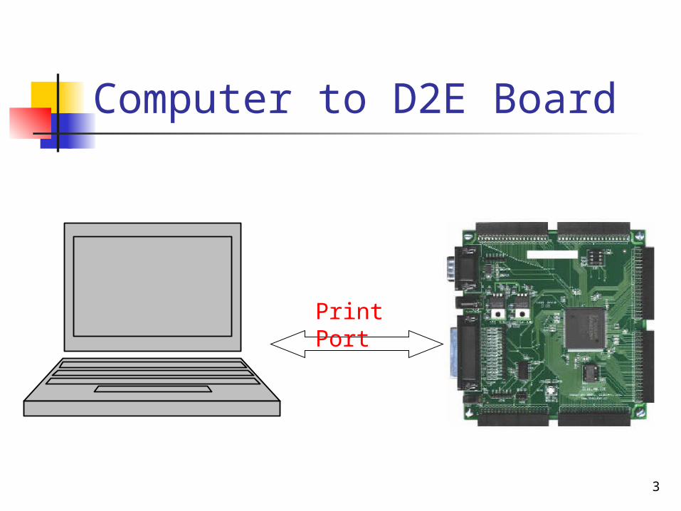
3
Computer to D2E Board
Print Port

4
Boards Interconnection~~
D2E Connect to DIO1
Port APort B
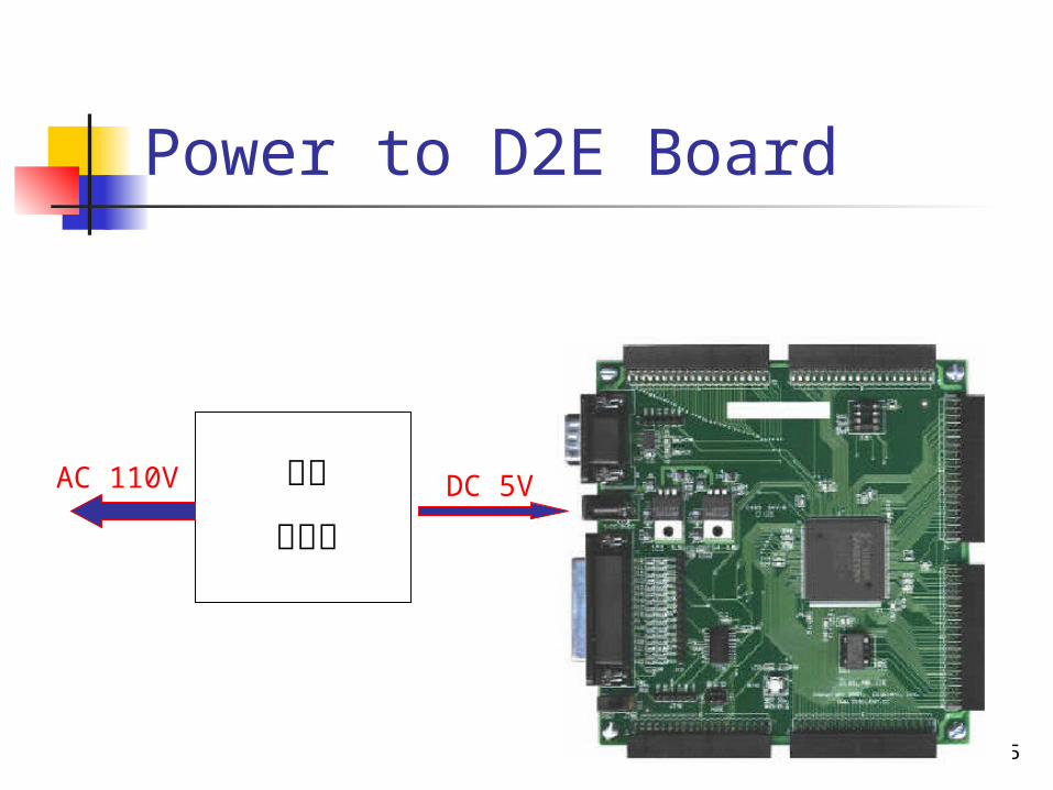
5
Power to D2E Board
變壓
整流器AC 110V DC 5V
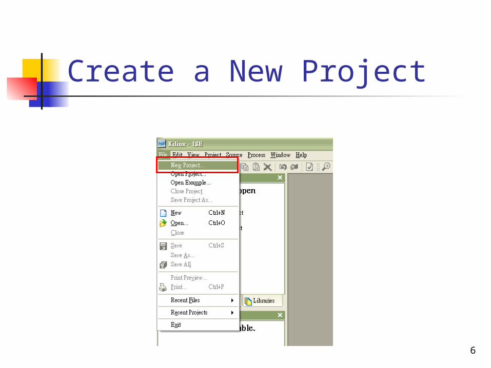
6
Create a New Project
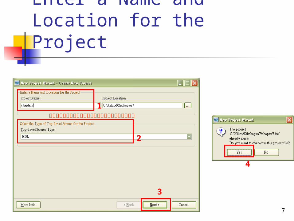
7
Enter a Name and Location for the Project
1
2
3
4
檔名開頭請勿使用數字或特殊符號並不要使用中文為檔名

8
Select Device Family, Package, Device and Speed Grade
1
2
9
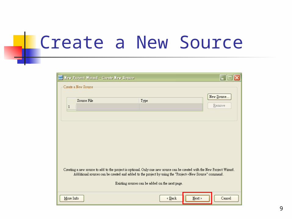
Create a New Source

1010
Next Step

1111
Finish

1212
Create a New File
13
2

1313
You can type Verilog on the New File

14
You can type Verilog on the New File
12
15
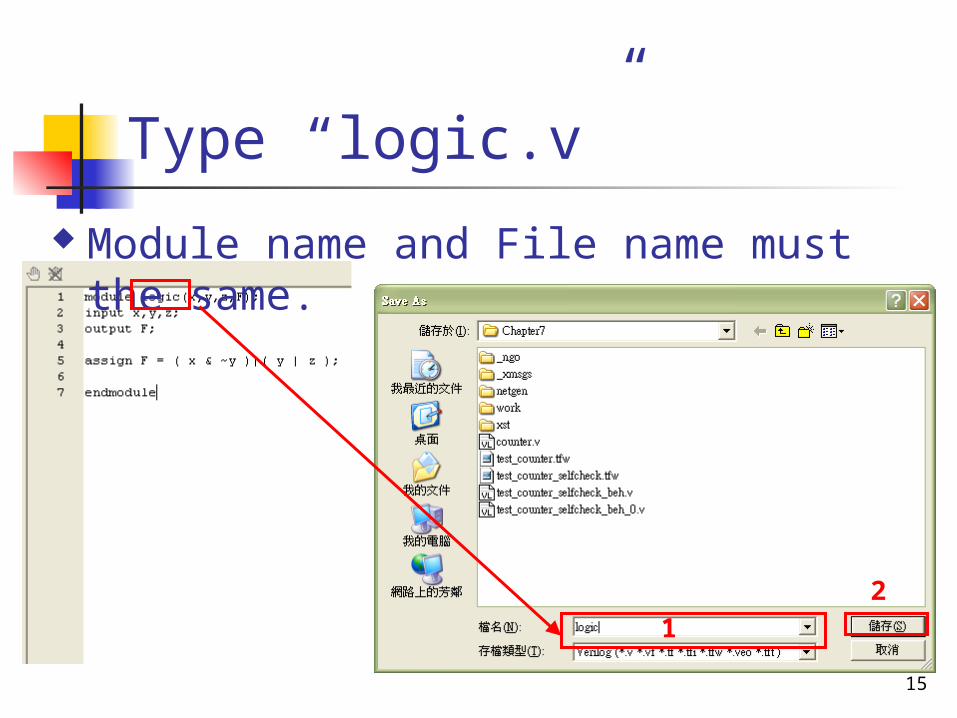
Type “logic.v”
Module name and File name must the same.
12

16
Add Source
1.Right Click
2

17
Select “logic.v”
1
23

18
Add Test Bench Waveform
1.Right Click
2
34
5
檔名開頭請勿使用數字或特殊符號並不要使用中文為檔名

Check Synthesize
Double Click

Select Source File
20
1
2

New Source Information
21

22
Select Design Type
1
2

Waveform Created by HDL Bencher
23

Select Behavioral Simulation
24
1
2

25
Give Input Value
1
2.Save

26
Generate Expected Simulation Result
Double Click2
27
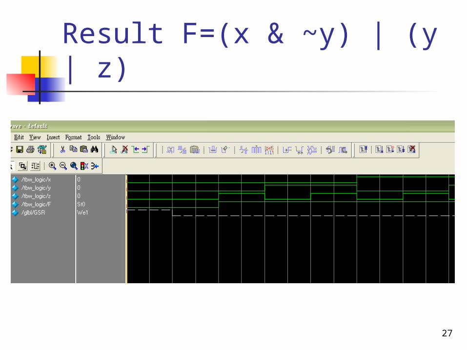
Result F=(x & ~y) | (y | z)

28
Add Implementation Constraints File
1.Right Click
2
3 4
5
檔名開頭請勿使用數字或特殊符號並不要使用中文為檔名

New Source Information
29

Select Synthesis/Implementation
30
21
31
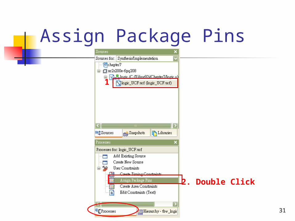
Assign Package Pins
2. Double Click
1
32
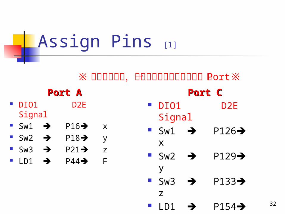
Assign Pins [1]
DIO1 D2E Signal
Sw1 P16 x Sw2 P18 y Sw3 P21 z LD1 P44 F
※請注意看板子,子板跟母板連接是使用哪一個 Port※
Port APort A DIO1 D2E
Signal Sw1 P126 x Sw2 P129 y Sw3 P133 z LD1 P154 F
Port CPort C

33
Assign pins [2]

34
Assign pins [3]
1
2. Save
3
4

35
Run “Implement Design”
1
2. Double Click

36
View/Edit Routed Design
Double Click

37
View Routed Design

38
Select FPGA Start-Up Clock to JTAG Clock
1. Right Click
2
3
4
3
4
5

39
Generate Bitstream File
Double Click

40
Run “Configure Device”
Double Click
此時請務必將版子接上

41
Select Boundary.. and Automatically…
2
1

42
Select “logic.bit file”
21
3

43
Right-click to select operation
21.Right Click
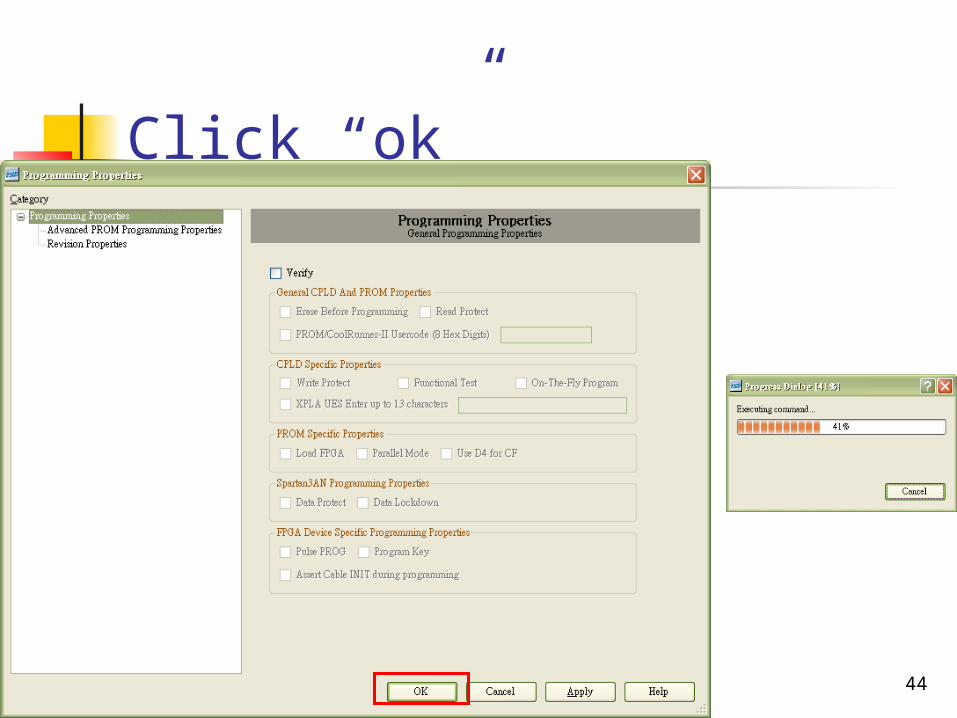
44
Click “ok”

45
Check the Results on Emulation Board

46
Question and Answer
歷史人物中,誰跑最快 ?