esd300-b1-02lrh - infineon
TRANSCRIPT

Power Management & Mult imarket
Data Sheet Revision 1.2, 2013-11-26Final
ESD300-B1-02LRHLow Clamping & Low Capacitance ESD/Surge Protection Diode
ESD300-B1-02LRH
TVS DiodeTransient Voltage Suppressor Diodes

ESD300-B1-02LRH
Final Data Sheet 2 Revision 1.2, 2013-11-26
Trademarks of Infineon Technologies AGAURIX™, BlueMoon™, C166™, CanPAK™, CIPOS™, CIPURSE™, COMNEON™, EconoPACK™, CoolMOS™,CoolSET™, CORECONTROL™, CROSSAVE™, DAVE™, EasyPIM™, EconoBRIDGE™, EconoDUAL™,EconoPIM™, EiceDRIVER™, eupec™, FCOS™, HITFET™, HybridPACK™, I²RF™, ISOFACE™, IsoPACK™,MIPAQ™, ModSTACK™, my-d™, NovalithIC™, OmniTune™, OptiMOS™, ORIGA™, PRIMARION™,PrimePACK™, PrimeSTACK™, PRO-SIL™, PROFET™, RASIC™, ReverSave™, SatRIC™, SIEGET™,SINDRION™, SIPMOS™, SMARTi™, SmartLEWIS™, SOLID FLASH™, TEMPFET™, thinQ!™,TRENCHSTOP™, TriCore™, X-GOLD™, X-PMU™, XMM™, XPOSYS™.
Other TrademarksAdvance Design System™ (ADS) of Agilent Technologies, AMBA™, ARM™, MULTI-ICE™, KEIL™,PRIMECELL™, REALVIEW™, THUMB™, µVision™ of ARM Limited, UK. AUTOSAR™ is licensed by AUTOSARdevelopment partnership. Bluetooth™ of Bluetooth SIG Inc. CAT-iq™ of DECT Forum. COLOSSUS™,FirstGPS™ of Trimble Navigation Ltd. EMV™ of EMVCo, LLC (Visa Holdings Inc.). EPCOS™ of Epcos AG.FLEXGO™ of Microsoft Corporation. FlexRay™ is licensed by FlexRay Consortium. HYPERTERMINAL™ ofHilgraeve Incorporated. IEC™ of Commission Electrotechnique Internationale. IrDA™ of Infrared DataAssociation Corporation. ISO™ of INTERNATIONAL ORGANIZATION FOR STANDARDIZATION. MATLAB™ ofMathWorks, Inc. MAXIM™ of Maxim Integrated Products, Inc. MICROTEC™, NUCLEUS™ of Mentor GraphicsCorporation. Mifare™ of NXP. MIPI™ of MIPI Alliance, Inc. MIPS™ of MIPS Technologies, Inc., USA. muRata™of MURATA MANUFACTURING CO., MICROWAVE OFFICE™ (MWO) of Applied Wave Research Inc.,OmniVision™ of OmniVision Technologies, Inc. Openwave™ Openwave Systems Inc. RED HAT™ Red Hat, Inc.RFMD™ RF Micro Devices, Inc. SIRIUS™ of Sirius Satellite Radio Inc. SOLARIS™ of Sun Microsystems, Inc.SPANSION™ of Spansion LLC Ltd. Symbian™ of Symbian Software Limited. TAIYO YUDEN™ of Taiyo YudenCo. TEAKLITE™ of CEVA, Inc. TEKTRONIX™ of Tektronix Inc. TOKO™ of TOKO KABUSHIKI KAISHA TA.UNIX™ of X/Open Company Limited. VERILOG™, PALLADIUM™ of Cadence Design Systems, Inc. VLYNQ™of Texas Instruments Incorporated. VXWORKS™, WIND RIVER™ of WIND RIVER SYSTEMS, INC. ZETEX™ ofDiodes Zetex Limited.Last Trademarks Update 2010-10-26
Revision History: Revision 1.1, 2013-06-17Page or Item Subjects (major changes since previous revision)Revision 1.2, 2013-11-264 Update of Figure 2-1)

ESD300-B1-02LRH
Low Clamping & Low Capacitance ESD/Surge Protection Diode
Final Data Sheet 3 Revision 1.2, 2013-11-26
1 Low Clamping & Low Capacitance ESD/Surge Protection Diode
1.1 Features
• Extremely high ESD and surge protection– IEC61000-4-2 (ESD): ±30 kV (air/contact discharge)– IEC61000-4-5 (surge): ±18 A (8/20 μs)
• Low clamping voltage VCL < 8 V (8 kV contact)• Maximum peak pulse power PPP = 260 W (8/20 μs)• Extremely low dynamic resistance: RDYN = 0.23 Ω typ.• Supports applications with signal voltage 3.3 V max.• Line capacitance: CL = typ. 1.2 pF• Package TSLP-2-17 compatible to SOD882D leadless ultra small Surface-Mounted Device (SMD)• Size 1 mm x 0.6 mm x 0.39 mm (0402)
1.2 Application Examples
• Reliable ESD and surge protection of highly susceptible IC/ASICs in computers and peripherals, audio, headset, human digital interfaces, video equipment, cellular handsets and accessories and portable electronics
• Dedicated solution to boost ESD and surge protection performance in miniaturized modern electronics• 10/100/1000 Ethernet
1.3 Product Description
Figure 1-1 Pin Configuration and Schematic Diagram
Table 1-1 Ordering InformationType Package Configuration Marking codeESD300-B1-02LRH TSLP-2-17 1 line, bi-directional S3
Configuration_Schematic_Diagram.vst.vsd
b) Schematic diagrama) Pin configuration
Pin 2
Pin 1
Pin 1 Pin 2
TSLP-2-17
Pin 1 Marking

ESD300-B1-02LRH
Characteristics
Final Data Sheet 4 Revision 1.2, 2013-11-26
2 Characteristics
2.1 Maximum Ratings
Attention: Stresses above the max. values listed here may cause permanent damage to the device. Exposure to absolute maximum rating conditions for extended periods may affect device reliability. Maximum ratings are absolute ratings; exceeding only one of these values may cause irreversible damage to the integrated circuit.
2.2 Electrical Characteristics at TA = 25 °C, unless otherwise specified
Figure 2-1 Definitions of electrical characteristics
Table 2-1 Maximum Ratings at TA = 25 °C, unless otherwise specified
Parameter Symbol Values UnitMin. Typ. Max.
ESD1)
contact dischargeair discharge
1) VESD according to IEC61000-4-2 (R = 330 , C = 150 pF discharge network)
VESD-30-30
--
3030
kV
Peak pulse current (tp = 8/20 μs)2)
2) IPP according to IEC61000-4-5 (tp = 8/20 μs)
IPP -18 - 18 APeak pulse power (tp = 8/20 μs)2) PPP - - 260 WOperating temperature range TOP -55 - 125 °CStorage temperature Tstg -65 - 150 °C
! !"#$

ESD300-B1-02LRH
Characteristics
Final Data Sheet 5 Revision 1.2, 2013-11-26
Table 2-2 DC Characteristics at TA = 25 °C, unless otherwise specified
Parameter Symbol Values Unit Note / Test ConditionMin. Typ. Max.
Reverse working voltage VRWM -3.3 - 3.3 VReverse current IR - - 100 nA VR = 3.3 V
Table 2-3 RF Characteristics at TA = 25 °C, unless otherwise specified
Parameter Symbol Values Unit Note / Test ConditionMin. Typ. Max.
Line capacitance CL - 1.2 1.8 pF VR = 0 V, f = 1 MHz
Table 2-4 ESD Characteristics at TA = 25 °C, unless otherwise specified
Parameter Symbol Values Unit Note / Test ConditionMin. Typ. Max.
Clamping voltage1)
1) VESD according to IEC61000-4-2 (R = 330 Ω, C = 150 pF discharge network)
VCL - 8 - V VESD = 8 kV, tp= 30 nscontact discharge
Clamping voltage2)
2) IPP according to IEC61000-4-5 (tp = 8/20 μs)
VCL---
58.510.5
---
V tp = 8/20 µsIPP = 1 AIPP = 12 AIPP = 18 A
Clamping voltage3)
--
9.512.5
--
tp = 100 nsIPP = 16 AIPP = 30 A
Dynamic resistance3)
3)ANSI/ESD STM5.5.1 - Electrostatic Discharge Sensitive Testing using Transmission Line Pulse (TLP) Model. TLP conditions: Z0 = 50 Ω, tp = 100 ns, tr = 0.6 ns, ITLP and VTLP averaging window: t1 = 30 ns to t2 = 60 ns, extraction of dynamic resistance using least squares fit of TLP characteristic between ITLP1 = 10 A and ITLP2 = 40 A. Please refer to Application Note AN210 [1]
RDYN - 0.23 - Ω

ESD300-B1-02LRH
Typical Characteristics at TA = 25 °C, unless otherwise specified
Final Data Sheet 6 Revision 1.2, 2013-11-26
3 Typical Characteristics at TA = 25 °C, unless otherwise specified
Figure 3-1 Reverse current: IR = f(VR)
Figure 3-2 Line capacitance: CL = f(VR), f = 1MHz
10-13
10-12
10-11
10-10
10-9
10-8
10-7
10-6
-3.5 -3 -2.5 -2 -1.5 -1 -0.5 0 0.5 1 1.5 2 2.5 3 3.5
I R [
mA
]
VR [V]
0
0.5
1
1.5
2
2.5
3
3.5
4
-3.5 -3 -2.5 -2 -1.5 -1 -0.5 0 0.5 1 1.5 2 2.5 3 3.5
CL [
pF
]
VR [V]

ESD300-B1-02LRH
Typical Characteristics at TA = 25 °C, unless otherwise specified
Final Data Sheet 7 Revision 1.2, 2013-11-26
Figure 3-3 Clamping voltage (TLP): ITLP = f(VTLP) according ANSI/ESD STM5.5.1 - Electrostatic Discharge Sensitivity Testing using Transmission Line Pulse (TLP) Model. TLP conditions: Z0 = 50 Ω, tp = 100 ns, tr = 0.6 ns, ITLP and VTLP averaging window: t1 = ns to t2 = 60 ns, extraction of dynamic resistance using squares fit to TLP characteristics between ITLP1 = 10 A and ITLP2 = 40 A. Please refer to Application Note AN210 [1]
-60
-50
-40
-30
-20
-10
0
10
20
30
40
50
60
-20 -15 -10 -5 0 5 10 15 20-30
-25
-20
-15
-10
-5
0
5
10
15
20
25
30
I TL
P [
A]
Eq
uiv
ale
nt
VIE
C
[kV
]
VTLP [V]
ESD300-B1-02LRHRDYN
RDYN = 0.223 Ω
RDYN = 0.227 Ω

ESD300-B1-02LRH
Typical Characteristics at TA = 25 °C, unless otherwise specified
Final Data Sheet 8 Revision 1.2, 2013-11-26
Figure 3-4 Pulse current (IEC61000-4-5) versus clamping voltage: IPP = f(VCL)
-25
-20
-15
-10
-5
0
5
10
15
20
25
-15 -10 -5 0 5 10 15
I PP [
A]
VCL [V]
ESD300-B1-02LRHRDYN
RDYN = 0.3 Ω
RDYN = 0.3 Ω

ESD300-B1-02LRH
Typical Characteristics at TA = 25 °C, unless otherwise specified
Final Data Sheet 9 Revision 1.2, 2013-11-26
Figure 3-5 IEC61000-4-2 : VCL = f(t), 8 kV positive pulse from pin 1 to pin 2
Figure 3-6 IEC61000-4-2 : VCL = f(t), 8 kV negative pulse from pin 1 to pin 2
-20
-10
0
10
20
30
40
50
60
70
-50 0 50 100 150 200 250 300 350 400 450
VC
L [
V]
tp [ns]
Scope: 6 GHz, 20 GS/s
VCL-max-peak = 64 V
VCL-30ns-peak = 8 V
-70
-60
-50
-40
-30
-20
-10
0
10
20
-50 0 50 100 150 200 250 300 350 400 450
VC
L [
V]
tp [ns]
Scope: 6 GHz, 20 GS/s
VCL-max-peak = -63 V
VCL-30ns-peak = -8 V
ESD300-B1-02LRH
Typical Characteristics at TA = 25 °C, unless otherwise specified
Final Data Sheet 10 Revision 1.2, 2013-11-26
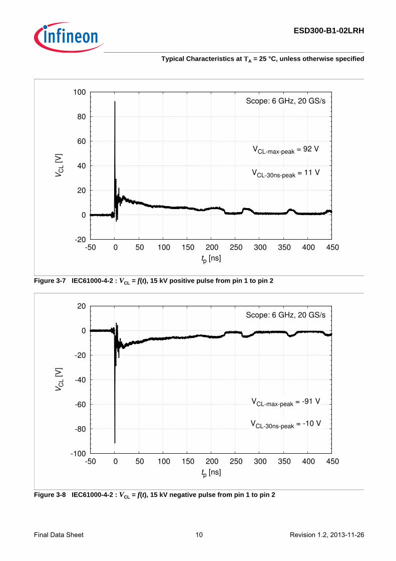
Figure 3-7 IEC61000-4-2 : VCL = f(t), 15 kV positive pulse from pin 1 to pin 2
Figure 3-8 IEC61000-4-2 : VCL = f(t), 15 kV negative pulse from pin 1 to pin 2
-20
0
20
40
60
80
100
-50 0 50 100 150 200 250 300 350 400 450
VC
L [
V]
tp [ns]
Scope: 6 GHz, 20 GS/s
VCL-max-peak = 92 V
VCL-30ns-peak = 11 V
-100
-80
-60
-40
-20
0
20
-50 0 50 100 150 200 250 300 350 400 450
VC
L [
V]
tp [ns]
Scope: 6 GHz, 20 GS/s
VCL-max-peak = -91 V
VCL-30ns-peak = -10 V

ESD300-B1-02LRH
Package Information
Final Data Sheet 11 Revision 1.2, 2013-11-26
4 Package Information
4.1 TSLP-2-17
Figure 4-1 TSLP-2-17 Package outline (dimension in mm)
Figure 4-2 TSLP-2-17 Footprint (dimension in mm)
Figure 4-3 TSLP-2-17 Packing (dimension in mm)
Figure 4-4 TSLP-2-17 Marking (example)
TSLP-2-7-PO V02
±0.050.6
1
2
±0.0
50.
65
±0.0
350.
251)
1±0.
05
0.05 MAX.
+0.010.39 -0.03
1) Dimension applies to plated terminal
Cathodemarking
1)±0.0350.5
Bottom viewTop view
TSLP-2-7-FP V01
0.45
0.27
50.
275
0.37
50.92
5
Copper Solder mask Stencil apertures
0.35
1
0.6
0.35
0.3
TSLP-2-7-TP V03
0.76
4
1.16
0.5
Orientationmarking
8
Type code
Cathode marking
TSLP-2-18-MK V01
12

ESD300-B1-02LRH
References
Final Data Sheet 12 Revision 1.2, 2013-11-26
References[1] Infineon AG - Application Note AN210: Effective ESD Protection design at System Level Using VF-TLP
Characterization Methodology
