trenchstoptm series - infineon technologies
TRANSCRIPT

Datasheet PleasereadtheImportantNoticeandWarningsattheendofthisdocument V2.1www.infineon.com 2017-02-09
AIKB20N60CT
TRENCHSTOPTMSeries
LowLossDuoPack:IGBTinTRENCHSTOPTMandFieldstoptechnologywithsoft,fastrecoveryanti-paralleldiodeFeatures:
•AutomotiveAECQ101qualified•DesignedforDC/ACconvertersforAutomotiveApplication•VerylowVCE(sat)1.5V(typ.)•MaximumJunctionTemperature150°C•Dynamicallystresstested•Shortcircuitwithstandtime5µs•PositivetemperaturecoefficientinVCE(sat)•LowEMI•LowGateCharge•GreenPackage•TRENCHSTOPTMandFieldstoptechnologyfor600Vapplicationsoffers:-verytightparameterdistribution-highruggedness,temperaturestablebehavior-veryhighswitchingspeed
Applications:
•Maininverter•Climatecompressor•PTCheater•Motordrives
G
C
E
G
E
C
KeyPerformanceandPackageParametersType VCE IC VCEsat,Tvj=25°C Tvjmax Marking PackageAIKB20N60CT 600V 20A 1.5V 150°C AK20DCT PG-TO263-3

Datasheet 2 V2.12017-02-09
AIKB20N60CT
TRENCHSTOPTMSeries
TableofContents
Description . . . . . . . . . . . . . . . . . . . . . . . . . . . . . . . . . . . . . . . . . . . . . . . . . . . . . . . . . . . . . . . . . . . . . . . . 1
Table of Contents . . . . . . . . . . . . . . . . . . . . . . . . . . . . . . . . . . . . . . . . . . . . . . . . . . . . . . . . . . . . . . . . . . . 2
Maximum Ratings . . . . . . . . . . . . . . . . . . . . . . . . . . . . . . . . . . . . . . . . . . . . . . . . . . . . . . . . . . . . . . . . . . . 3
Thermal Resistance . . . . . . . . . . . . . . . . . . . . . . . . . . . . . . . . . . . . . . . . . . . . . . . . . . . . . . . . . . . . . . . . . 3
Electrical Characteristics . . . . . . . . . . . . . . . . . . . . . . . . . . . . . . . . . . . . . . . . . . . . . . . . . . . . . . . . . . . . . . 4
Electrical Characteristics Diagrams . . . . . . . . . . . . . . . . . . . . . . . . . . . . . . . . . . . . . . . . . . . . . . . . . . . . . 6
Package Drawing . . . . . . . . . . . . . . . . . . . . . . . . . . . . . . . . . . . . . . . . . . . . . . . . . . . . . . . . . . . . . . . . . . .13
Testing Conditions . . . . . . . . . . . . . . . . . . . . . . . . . . . . . . . . . . . . . . . . . . . . . . . . . . . . . . . . . . . . . . . . . .14
Revision History . . . . . . . . . . . . . . . . . . . . . . . . . . . . . . . . . . . . . . . . . . . . . . . . . . . . . . . . . . . . . . . . . . . .15
Disclaimer . . . . . . . . . . . . . . . . . . . . . . . . . . . . . . . . . . . . . . . . . . . . . . . . . . . . . . . . . . . . . . . . . . . . . . . . .16

Datasheet 3 V2.12017-02-09
AIKB20N60CT
TRENCHSTOPTMSeries
MaximumRatings
Parameter Symbol Value UnitCollector-emittervoltage,Tvj≥25°C VCE 600 V
DCcollectorcurrent,limitedbyTvjmaxTC=25°CTC=100°C
IC 40.020.0
A
Pulsedcollectorcurrent,tplimitedbyTvjmax ICpuls 60.0 A
TurnoffsafeoperatingareaVCE≤600V,Tvj≤150°C1) - 60.0 A
Diodeforwardcurrent,limitedbyTvjmaxTC=25°CTC=100°C
IF 40.020.0
A
Diodepulsedcurrent,tplimitedbyTvjmax IFpuls 60.0 A
Gate-emitter voltage VGE ±20 V
Short circuit withstand timeVGE=15.0V,VCC≤400VAllowed number of short circuits < 1000Time between short circuits: ≥ 1.0sTvj=150°C
tSC
5
µs
PowerdissipationTC=25°C Ptot 156.0 W
Operating junction temperature Tvj -40...+150 °C
Storage temperature Tstg -40...+150 °C
Soldering temperature,reflow soldering (MSL1 according to JEDEC J-STA-020) 260 °C
ThermalResistance
Valuemin. typ. max.
Parameter Symbol Conditions Unit
RthCharacteristics
IGBT thermal resistance,junction - case Rth(j-c) - - 0.90 K/W
Diode thermal resistance,junction - case Rth(j-c) - - 1.50 K/W
Thermal resistance, min. footprintjunction - ambient Rth(j-a) - - 65 K/W
Thermal resistance, 6cm² Cu onPCBjunction - ambient
Rth(j-a) - - 40 K/W
1) tp≤1µs

Datasheet 4 V2.12017-02-09
AIKB20N60CT
TRENCHSTOPTMSeries
ElectricalCharacteristic,atTvj=25°C,unlessotherwisespecified
Valuemin. typ. max.
Parameter Symbol Conditions Unit
StaticCharacteristic
Collector-emitter breakdown voltage V(BR)CES VGE=0V,IC=0.20mA 600 - - V
Collector-emitter saturation voltage VCEsat
VGE=15.0V,IC=20.0ATvj=25°CTvj=150°C
--
1.501.85
2.05-
V
Diode forward voltage VF
VGE=0V,IF=20.0ATvj=25°CTvj=150°C
--
1.651.65
2.05-
V
Gate-emitter threshold voltage VGE(th) IC=0.29mA,VCE=VGE 4.1 4.9 5.7 V
Zero gate voltage collector current ICESVCE=600V,VGE=0VTvj=25°CTvj=150°C
--
-550
40-
µA
Gate-emitter leakage current IGES VCE=0V,VGE=20V - - 100 nA
Transconductance gfs VCE=20V,IC=20.0A - 11.0 - S
Integrated gate resistor rG none Ω
ElectricalCharacteristic,atTvj=25°C,unlessotherwisespecified
Valuemin. typ. max.
Parameter Symbol Conditions Unit
DynamicCharacteristic
Input capacitance Cies - 1100 -
Output capacitance Coes - 71 -
Reverse transfer capacitance Cres - 32 -
VCE=25V,VGE=0V,f=1MHz pF
Gate charge QGVCC=480V,IC=20.0A,VGE=15V - 120.0 - nC
Internal emitter inductancemeasured 5mm (0.197 in.) fromcase
LE - 7.0 - nH
Short circuit collector currentMax. 1000 short circuitsTime between short circuits: ≥ 1.0s
IC(SC)VGE=15.0V,VCC≤400V,tSC≤5µsTvj=150°C
- 183 - A
SwitchingCharacteristic,InductiveLoad
Valuemin. typ. max.
Parameter Symbol Conditions Unit
IGBTCharacteristic,atTvj=25°CTurn-on delay time td(on) - 18 - ns
Rise time tr - 14 - ns
Turn-off delay time td(off) - 199 - ns
Fall time tf - 42 - ns
Turn-on energy Eon - 0.31 - mJ
Turn-off energy Eoff - 0.46 - mJ
Total switching energy Ets - 0.77 - mJ
Tvj=25°C,VCC=600V,IC=20.0A,VGE=0.0/15.0V,RG(on)=12.0Ω,RG(off)=12.0Ω,Lσ=131nH,Cσ=31pFLσ,CσfromFig.EEnergy losses include “tail” anddiode reverse recovery.

Datasheet 5 V2.12017-02-09
AIKB20N60CT
TRENCHSTOPTMSeries
DiodeCharacteristic,atTvj=25°C
Diode reverse recovery time trr - 41 - ns
Diode reverse recovery charge Qrr - 0.31 - µC
Diode peak reverse recovery current Irrm - 13.3 - A
Diode peak rate of fall of reverserecoverycurrentduringtb dirr/dt - 711 - A/µs
Tvj=25°C,VR=600V,IF=20.0A,diF/dt=880A/µs
SwitchingCharacteristic,InductiveLoad
Valuemin. typ. max.
Parameter Symbol Conditions Unit
IGBTCharacteristic,atTvj=150°CTurn-on delay time td(on) - 18 - ns
Rise time tr - 17 - ns
Turn-off delay time td(off) - 217 - ns
Fall time tf - 70 - ns
Turn-on energy Eon - 0.47 - mJ
Turn-off energy Eoff - 0.60 - mJ
Total switching energy Ets - 1.07 - mJ
Tvj=150°C,VCC=600V,IC=20.0A,VGE=0.0/15.0V,RG(on)=12.0Ω,RG(off)=12.0Ω,Lσ=131nH,Cσ=31pFLσ,CσfromFig.EEnergy losses include “tail” anddiode reverse recovery.
DiodeCharacteristic,atTvj=150°C
Diode reverse recovery time trr - 201 - ns
Diode reverse recovery charge Qrr - 1.28 - µC
Diode peak reverse recovery current Irrm - 16.6 - A
Diode peak rate of fall of reverserecoverycurrentduringtb dirr/dt - 481 - A/µs
Tvj=150°C,VR=600V,IF=20.0A,diF/dt=800A/µs
Datasheet 6 V2.12017-02-09
AIKB20N60CT
TRENCHSTOPTMSeries
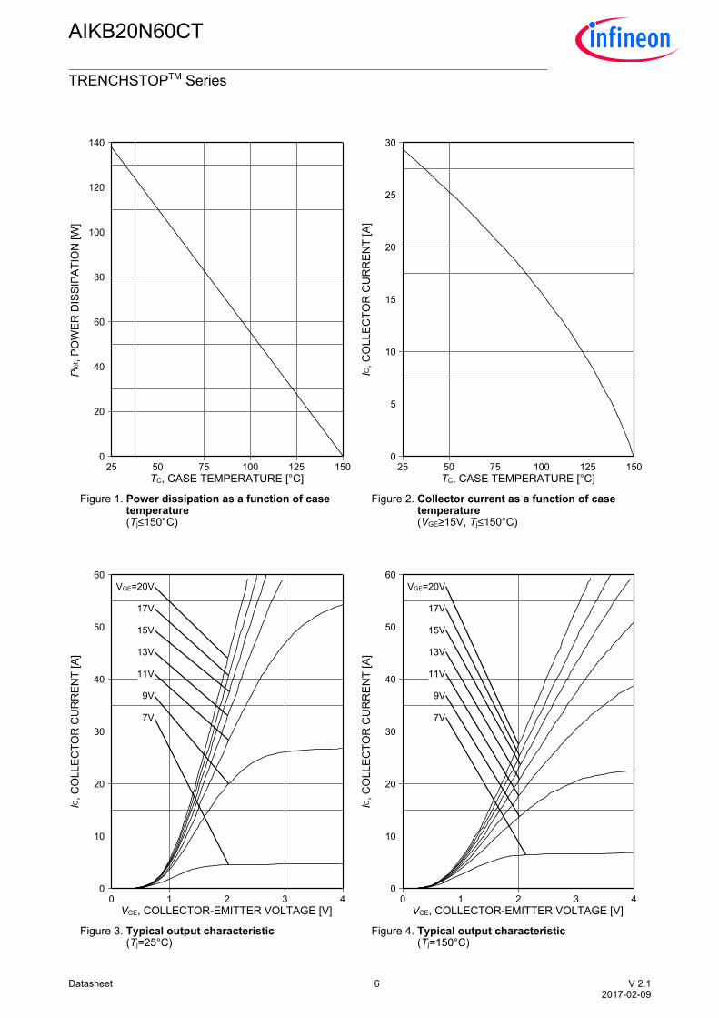
Figure 1. Powerdissipationasafunctionofcasetemperature(Tj≤150°C)
TC,CASETEMPERATURE[°C]
Ptot ,POWERDISSIPATION[W
]
25 50 75 100 125 1500
20
40
60
80
100
120
140
Figure 2. Collectorcurrentasafunctionofcasetemperature(VGE≥15V,Tj≤150°C)
TC,CASETEMPERATURE[°C]
IC,C
OLLECTO
RCURRENT[A]
25 50 75 100 125 1500
5
10
15
20
25
30
Figure 3. Typicaloutputcharacteristic(Tj=25°C)
VCE,COLLECTOR-EMITTERVOLTAGE[V]
IC,C
OLLECTO
RCURRENT[A]
0 1 2 3 40
10
20
30
40
50
60VGE=20V
17V
15V
13V
11V
9V
7V
Figure 4. Typicaloutputcharacteristic(Tj=150°C)
VCE,COLLECTOR-EMITTERVOLTAGE[V]
IC,C
OLLECTO
RCURRENT[A]
0 1 2 3 40
10
20
30
40
50
60VGE=20V
17V
15V
13V
11V
9V
7V

Datasheet 7 V2.12017-02-09
AIKB20N60CT
TRENCHSTOPTMSeries
Figure 5. Typicaltransfercharacteristic(VCE=10V)
VGE,GATE-EMITTERVOLTAGE[V]
IC,C
OLLECTO
RCURRENT[A]
0 2 4 6 8 100
5
10
15
20
25
30
35
4025°CTj=150°C
Figure 6. Typicalcollector-emittersaturationvoltageasafunctionofjunctiontemperature(VGE=15V)
Tj,JUNCTIONTEMPERATURE[°C]
VCE(sat) ,COLLECTO
R-EMITTE
RSATU
RATION[A
]
0 50 100 1500.0
0.5
1.0
1.5
2.0
2.5
3.0IC=10AIC=20AIC=40A
Figure 7. Typicalswitchingtimesasafunctionofcollectorcurrent(inductiveload,Tj=150°C,VCE=400V,VGE=15/0V,RG=12Ω,DynamictestcircuitinFigure E)
IC,COLLECTORCURRENT[A]
t,SWITCHINGTIMES[ns]
0 5 10 15 20 25 30 35 401
10
100
1000td(off)
tftd(on)
tr
Figure 8. Typicalswitchingtimesasafunctionofgateresistor(inductiveload,Tj=150°C,VCE=400V,VGE=15/0V,IC=20A,DynamictestcircuitinFigure E)
RG,GATERESISTOR[Ω]
t,SWITCHINGTIMES[ns]
0 10 20 30 40 50 60 7010
100
1000td(off)
tftd(on)
tr

Datasheet 8 V2.12017-02-09
AIKB20N60CT
TRENCHSTOPTMSeries
Figure 9. Typicalswitchingtimesasafunctionofjunctiontemperature(inductiveload,VCE=400V,VGE=15/0V,IC=20A,RG=12Ω,DynamictestcircuitinFigure E)
TG,JUNCTIONTEMPERATURE[°C]
t,SWITCHINGTIMES[ns]
25 50 75 100 125 15010
100
1000td(off)
tftd(on)
tr
Figure 10. Gate-emitterthresholdvoltageasafunctionofjunctiontemperature(IC=0.29mA)
TG,JUNCTIONTEMPERATURE[°C]
VGE(th) ,GATE
-EMITTE
RTHRESHOLD
VOLTAGE[V
]
-50 0 50 100 1500
1
2
3
4
5
6
7typ.
Figure 11. Typicalswitchingenergylossesasafunctionofcollectorcurrent(inductiveload,Tj=150°C,VCE=400V,VGE=15/0V,RG=12Ω,DynamictestcircuitinFigure E)
IC,COLLECTORCURRENT[A]
E,S
WITCHINGENERGYLOSSES[m
J]
0 5 10 15 20 25 30 35 400.0
0.4
0.8
1.2
1.6
2.0
2.4
Eoff
Eon*Ets*
Figure 12. Typicalswitchingenergylossesasafunctionofgateresistor(inductiveload,Tj=150°C,VCE=400V,VGE=15/0V,IC=20A,DynamictestcircuitinFigure E)
RG,GATERESISTOR[Ω]
E,S
WITCHINGENERGYLOSSES[m
J]
0 10 20 30 40 50 60 700.0
0.4
0.8
1.2
1.6
2.0
2.4
Eoff
Eon*Ets*
Datasheet 9 V2.12017-02-09
AIKB20N60CT
TRENCHSTOPTMSeries
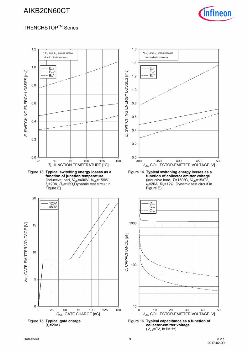
Figure 13. Typicalswitchingenergylossesasafunctionofjunctiontemperature(inductiveload,VCE=400V,VGE=15/0V,IC=20A,RG=12Ω,DynamictestcircuitinFigure E)
Tj,JUNCTIONTEMPERATURE[°C]
E,S
WITCHINGENERGYLOSSES[m
J]
25 50 75 100 125 1500.0
0.2
0.4
0.6
0.8
1.0
1.2
Eoff
Eon*Ets*
Figure 14. Typicalswitchingenergylossesasafunctionofcollectoremittervoltage(inductiveload,Tj=150°C,VGE=15/0V,IC=20A,RG=12Ω,DynamictestcircuitinFigure E)
VCE,COLLECTOR-EMITTERVOLTAGE[V]
E,S
WITCHINGENERGYLOSSES[m
J]
300 350 400 450 5000.0
0.2
0.4
0.6
0.8
1.0
1.2
1.4
1.6
Eoff
Eon*Ets*
Figure 15. Typicalgatecharge(IC=20A)
QGE,GATECHARGE[nC]
VGE,G
ATE
-EMITTE
RVOLTAGE[V
]
0 25 50 75 100 125 1500
5
10
15
20120V480V
Figure 16. Typicalcapacitanceasafunctionofcollector-emittervoltage(VGE=0V,f=1MHz)
VCE,COLLECTOR-EMITTERVOLTAGE[V]
C,C
APACITANCE[pF]
0 10 20 30 40 5010
100
1000
Ciss
Coss
Crss
Datasheet 10 V2.12017-02-09
AIKB20N60CT
TRENCHSTOPTMSeries
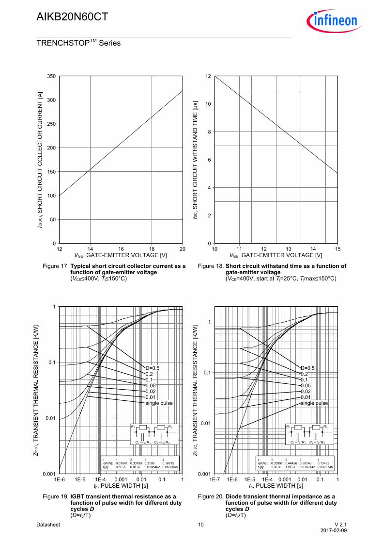
Figure 17. Typicalshortcircuitcollectorcurrentasafunctionofgate-emittervoltage(VCE≤400V,Tj≤150°C)
VGE,GATE-EMITTERVOLTAGE[V]
IC(SC) ,SHORTCIRCUITCOLLECTO
RCURRENT[A]
12 14 16 18 200
50
100
150
200
250
300
350
Figure 18. Shortcircuitwithstandtimeasafunctionofgate-emittervoltage(VCE=400V,startatTj=25°C,Tjmax≤150°C)
VGE,GATE-EMITTERVOLTAGE[V]
tSC,S
HORTCIRCUITW
ITHSTA
NDTIME[µs]
10 11 12 13 14 150
2
4
6
8
10
12
Figure 19. IGBTtransientthermalresistanceasafunctionofpulsewidthfordifferentdutycyclesD(D=tp/T)
tp,PULSEWIDTH[s]
ZthJC,TRANSIENTTH
ERMALRESISTA
NCE[K
/W]
1E-6 1E-5 1E-4 0.001 0.01 0.1 10.001
0.01
0.1
1
D=0.50.20.10.050.020.01single pulse
i:ri[K/W]:τi[s]:
10.070419.6E-5
20.307096.8E-4
30.31990.0108462
40.187150.0692548
Figure 20. DiodetransientthermalimpedanceasafunctionofpulsewidthfordifferentdutycyclesD(D=tp/T)
tp,PULSEWIDTH[s]
ZthJC,TRANSIENTTH
ERMALRESISTA
NCE[K
/W]
1E-7 1E-6 1E-5 1E-4 0.001 0.01 0.1 10.001
0.01
0.1
1
D=0.50.20.10.050.020.01single pulse
i:ri[K/W]:τi[s]:
10.339971.3E-4
20.444561.5E-3
30.581460.0182142
40.134830.0920745

Datasheet 11 V2.12017-02-09
AIKB20N60CT
TRENCHSTOPTMSeries
Figure 21. Typicalreverserecoverytimeasafunctionofdiodecurrentslope(VR=400V,DynamictestcircuitinFigureE)
diF/dt,DIODECURRENTSLOPE[A/µs]
trr,R
EVERSERECOVERYTIME[ns]
600 900 1200 15000
50
100
150
200
250
300Tj=25°C, IF = 20ATj=150°C, IF = 20A
Figure 22. Typicalreverserecoverychargeasafunctionofdiodecurrentslope(VR=400V,DynamictestcircuitinFigureE)
diF/dt,DIODECURRENTSLOPE[A/µs]
Qrr,R
EVERSERECOVERYCHARGE[µC]
600 900 1200 15000.0
0.2
0.4
0.6
0.8
1.0
1.2
1.4
1.6Tj=25°C, IF = 20ATj=150°C, IF = 20A
Figure 23. Typicalreverserecoverycurrentasafunctionofdiodecurrentslope(VR=400V,DynamictestcircuitinFigureE)
diF/dt,DIODECURRENTSLOPE[A/µs]
Irr,R
EVERSERECOVERYCURRENT[A]
600 900 1200 15000
5
10
15
20
25Tj=25°C, IF = 20ATj=150°C, IF = 20A
Figure 24. Typicaldiodepeakrateoffallofreverserecoverycurrentasafunctionofdiodecurrentslope(VR=400V,DynamictestcircuitinFigureE)
diF/dt,DIODECURRENTSLOPE[A/µs]
dIrr/dt,diodepeakrateoffallofI
rr[A
/µs]
600 900 1200 1500-900
-750
-600
-450
-300
-150
0Tj=25°C, IF = 20ATj=150°C, IF = 20A

Datasheet 12 V2.12017-02-09
AIKB20N60CT
TRENCHSTOPTMSeries
Figure 25. Typicaldiodeforwardcurrentasafunctionofforwardvoltage
VF,FORWARDVOLTAGE[V]
IF ,FORWARDCURRENT[A]
0.0 0.5 1.0 1.5 2.0 2.50
10
20
30
40
50
60Tj=25°CTj=150°C
Figure 26. Typicaldiodeforwardvoltageasafunctionofjunctiontemperature
Tj,JUNCTIONTEMPERATURE[°C]
VF ,FO
RWARDVOLTAGE[V
]
0 50 100 1500.0
0.5
1.0
1.5
2.0
2.5IC=10AIC=20AIC=40A

Datasheet 13 V2.12017-02-09
AIKB20N60CT
TRENCHSTOPTMSeries
01
30-08-2007
Z8B00003324
0.039
0.000
0.026
0.335
0.013
0.037
MIN
0.169
0.046
0.280
0.090
0.386
8.60 0.3390.256
0.575
0.632
0.366
0.177
0.421
0.049
0.144
5.08
2.54
1.00
7.10
2.29
9.80
6.50
9.30
4.50
14.61
16.05
10.70
1.25
3.65
0.70
2
0.00
0.65
0.33
8.51
0.95
4.30
MIN
1.17
1.60
1.78
7.90
10.31
3.00
15.88
16.25
9.50
4.70
10.90
1.45
3.85
MAX
4.57
0.25
1.15
0.65
9.45
0.85
1.40
0.200
0.100
0.028
2
0.063
0.070
0.311
0.406
0.118
0.625
0.640
0.374
0.185
0.429
0.057
0.152
0.010
0.180
0.033
0.026
0.372
0.045
MAX
0.055
0
7.5mm
55
0
Package Drawing PG-TO263-3
Datasheet 14 V2.12017-02-09
AIKB20N60CT
TRENCHSTOPTMSeries
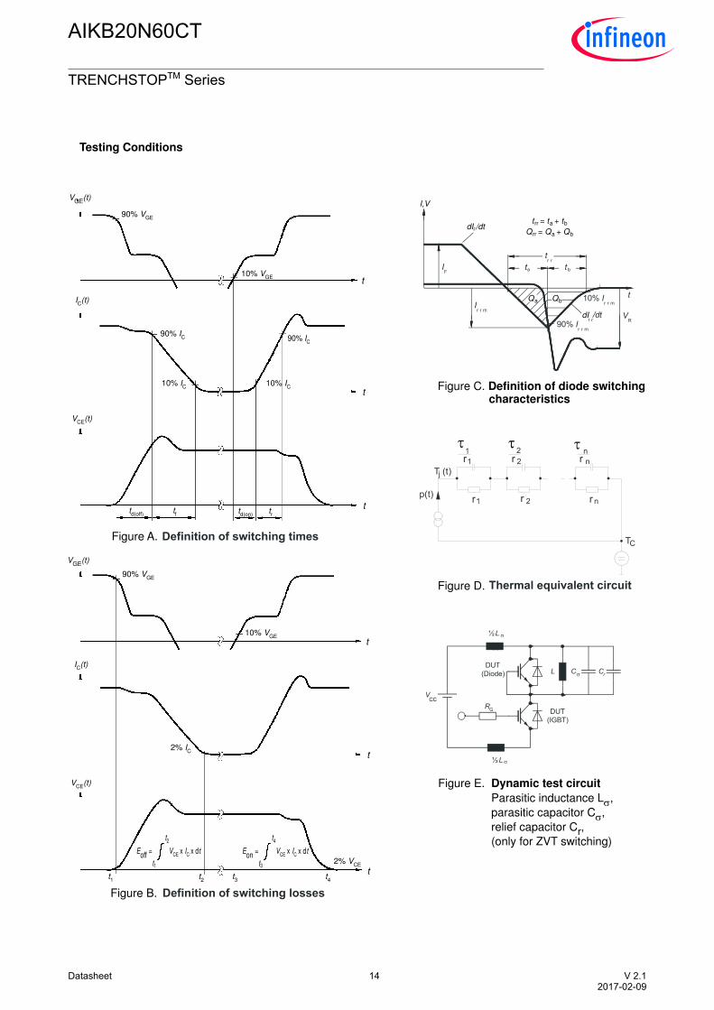
t
a b
td(off)
tf t
rtd(on)
90% IC
10% IC
90% IC
10% VGE
10% IC
t
90% VGE
t
t
90% VGE
VGE
(t)
t
t
tt1 t
4
2% IC
10% VGE
2% VCE
t2
t3
E
t
t
V I toff
= x x d
1
2
CE CE
t
t
V I ton
= x x d
3
4
CE C
CC
dI /dtF
dI
I,V
Figure A.
Figure B.
Figure C. Definition of diode switchingcharacteristics
Figure E. Dynamic test circuit
Figure D.
I (t)C
Parasitic inductance L ,
parasitic capacitor C ,
relief capacitor C ,
(only for ZVT switching)
s
s
r
t t t
Q Q Qrr a b
rr a b
= +
= +
Qa Qb
V (t)CE
VGE
(t)
I (t)C
V (t)CE
Testing Conditions

Datasheet 15 V2.12017-02-09
AIKB20N60CT
TRENCHSTOPTMSeries
RevisionHistory
AIKB20N60CT
Revision:2017-02-09,Rev.2.1Previous Revision
Revision Date Subjects (major changes since last revision)
2.1 2017-02-09 Data sheet created

TrademarksofInfineonTechnologiesAGµHVIC™,µIPM™,µPFC™,AU-ConvertIR™,AURIX™,C166™,CanPAK™,CIPOS™,CIPURSE™,CoolDP™,CoolGaN™,COOLiR™,CoolMOS™,CoolSET™,CoolSiC™,DAVE™,DI-POL™,DirectFET™,DrBlade™,EasyPIM™,EconoBRIDGE™,EconoDUAL™,EconoPACK™,EconoPIM™,EiceDRIVER™,eupec™,FCOS™,GaNpowIR™,HEXFET™,HITFET™,HybridPACK™,iMOTION™,IRAM™,ISOFACE™,IsoPACK™,LEDrivIR™,LITIX™,MIPAQ™,ModSTACK™,my-d™,NovalithIC™,OPTIGA™,OptiMOS™,ORIGA™,PowIRaudio™,PowIRStage™,PrimePACK™,PrimeSTACK™,PROFET™,PRO-SIL™,RASIC™,REAL3™,SmartLEWIS™,SOLIDFLASH™,SPOC™,StrongIRFET™,SupIRBuck™,TEMPFET™,TRENCHSTOP™,TriCore™,UHVIC™,XHP™,XMC™TrademarksupdatedNovember2015OtherTrademarksAllreferencedproductorservicenamesandtrademarksarethepropertyoftheirrespectiveowners.
PublishedbyInfineonTechnologiesAG81726München,Germany©InfineonTechnologiesAG2017.AllRightsReserved.
ImportantNoticeTheinformationgiveninthisdocumentshallinnoeventberegardedasaguaranteeofconditionsorcharacteristics(“Beschaffenheitsgarantie”).Withrespecttoanyexamples,hintsoranytypicalvaluesstatedhereinand/oranyinformationregardingtheapplicationoftheproduct,InfineonTechnologiesherebydisclaimsanyandallwarrantiesandliabilitiesofanykind,includingwithoutlimitationwarrantiesofnon-infringementofintellectualpropertyrightsofanythirdparty.
Inaddition,anyinformationgiveninthisdocumentissubjecttocustomer’scompliancewithitsobligationsstatedinthisdocumentandanyapplicablelegalrequirements,normsandstandardsconcerningcustomer’sproductsandanyuseoftheproductofInfineonTechnologiesincustomer’sapplications.
Thedatacontainedinthisdocumentisexclusivelyintendedfortechnicallytrainedstaff.Itistheresponsibilityofcustomer’stechnicaldepartmentstoevaluatethesuitabilityoftheproductfortheintendedapplicationandthecompletenessoftheproductinformationgiveninthisdocumentwithrespecttosuchapplication.
Forfurtherinformationontheproduct,technology,deliverytermsandconditionsandpricespleasecontactyournearestInfineonTechnologiesoffice(www.infineon.com).
WarningsDuetotechnicalrequirementsproductsmaycontaindangeroussubstances.ForinformationonthetypesinquestionpleasecontactyournearestInfineonTechnologiesoffice.
ExceptasotherwiseexplicitlyapprovedbyInfineonTechnologiesinawrittendocumentsignedbyauthorizedrepresentativesofInfineonTechnologies,InfineonTechnologies’productsmaynotbeusedinanyapplicationswhereafailureoftheproductoranyconsequencesoftheusethereofcanreasonablybeexpectedtoresultinpersonalinjury.