Архитектура stm32l0objectives •introduce stm32l0 internal structure •briefly describe...
TRANSCRIPT
Архитектура STM32L0
Александр КВАШИН
Роман ПОПОВ
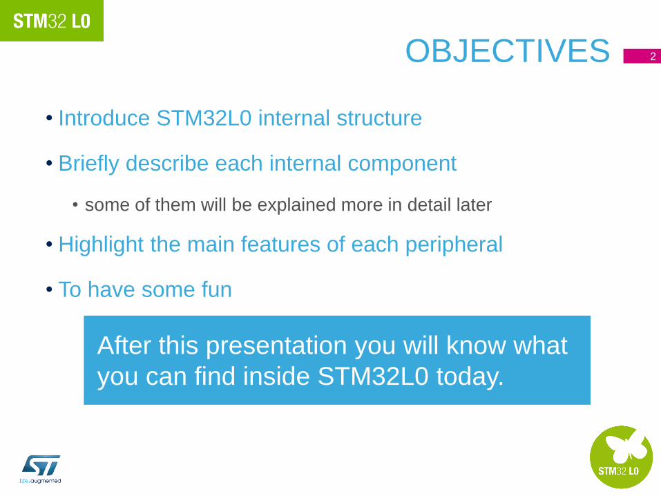
OBJECTIVES
• Introduce STM32L0 internal structure
• Briefly describe each internal component
• some of them will be explained more in detail later
• Highlight the main features of each peripheral
• To have some fun
2
After this presentation you will know what
you can find inside STM32L0 today.
Introduction
3
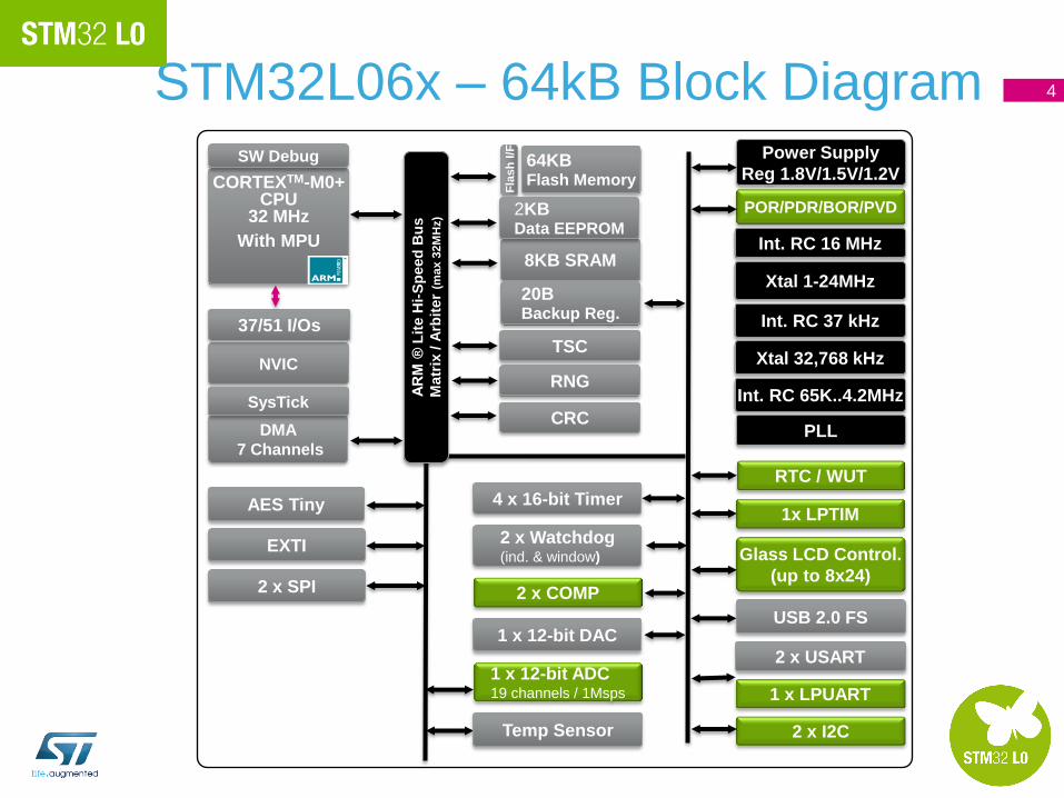
STM32L06x – 64kB Block Diagram
CORTEXTM-M0+ CPU
32 MHz
With MPU 8KB SRAM
2 x I2C
2 x USART
SW Debug Power Supply
Reg 1.8V/1.5V/1.2V
DMA
7 Channels
NVIC
2 x SPI
SysTick A
RM
® L
ite
Hi-
Sp
eed
Bu
s
Matr
ix / A
rbit
er
(max 3
2M
Hz)
PLL
RTC / WUT
20B Backup Reg.
Fla
sh
I/F
64KB Flash Memory
2KB Data EEPROM
USB 2.0 FS
Glass LCD Control.
(up to 8x24)
Int. RC 16 MHz
Xtal 1-24MHz
Int. RC 37 kHz
Xtal 32,768 kHz
Int. RC 65K..4.2MHz
EXTI
AES Tiny
1 x 12-bit ADC 19 channels / 1Msps
Temp Sensor
4 x 16-bit Timer
1 x 12-bit DAC
2 x COMP
2 x Watchdog (ind. & window)
4
TSC
RNG
37/51 I/Os
1x LPTIM
1 x LPUART
POR/PDR/BOR/PVD
CRC
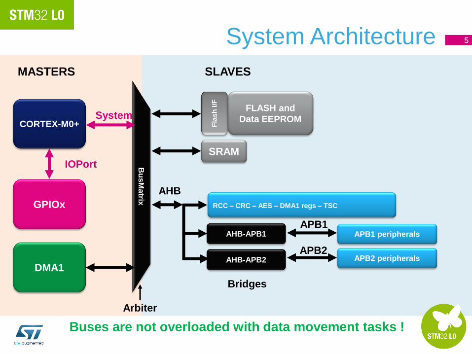
System Architecture
Buses are not overloaded with data movement tasks ! B
usM
atrix
System
CORTEX-M0+
DMA1
SRAM
FLASH and
Data EEPROM
Fla
sh
I/F
AHB-APB1
AHB-APB2
AHB
APB1 peripherals
Bridges
APB2
APB1
Arbiter
RCC – CRC – AES – DMA1 regs – TSC
APB2 peripherals
GPIOx
MASTERS SLAVES
5
IOPort

6 BUS MATRIX
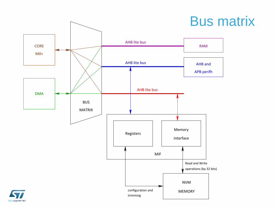
Bus matrix
AHB lite bus
configuration and
trimmingMEMORY
NVM
Read and Write
operations (by 32 bits)
Memory
interfaceRegisters
MIF
CORE
M0+
DMA
RAMAHB lite bus
MATRIX
BUS
APB perifh
AHB andAHB lite bus
System blocks
8
System blocks
Core
9
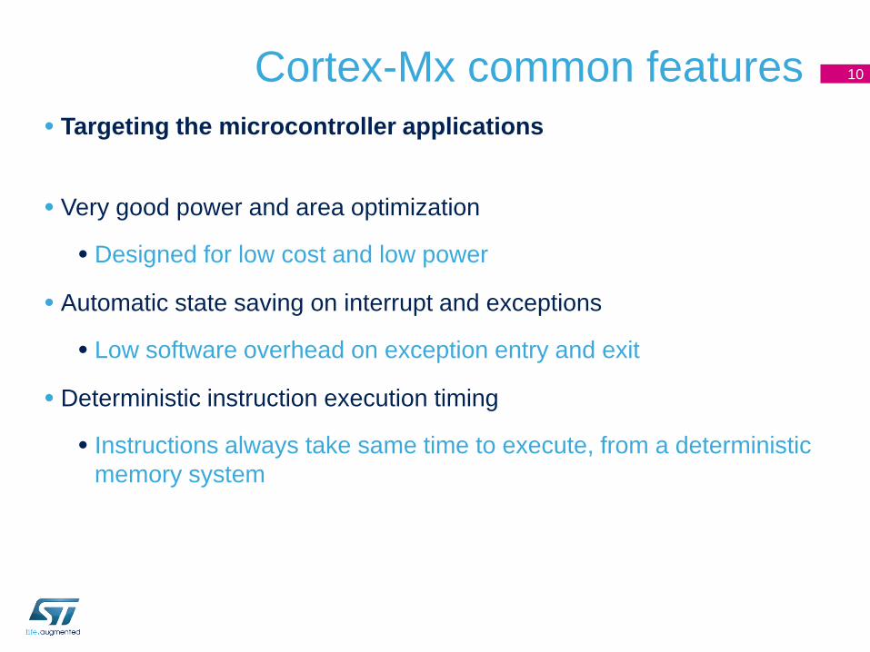
Cortex-Mx common features
• Targeting the microcontroller applications
• Very good power and area optimization
• Designed for low cost and low power
• Automatic state saving on interrupt and exceptions
• Low software overhead on exception entry and exit
• Deterministic instruction execution timing
• Instructions always take same time to execute, from a deterministic
memory system
10
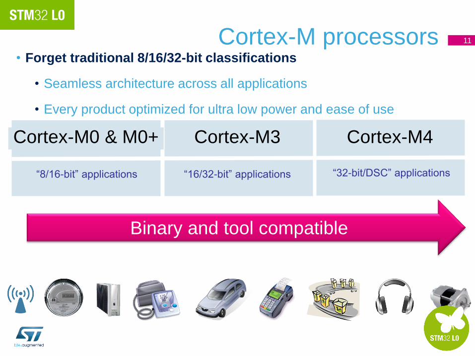
Cortex-M processors • Forget traditional 8/16/32-bit classifications
• Seamless architecture across all applications
• Every product optimized for ultra low power and ease of use
Cortex-M0 & M0+ Cortex-M3 Cortex-M4
“8/16-bit” applications “16/32-bit” applications “32-bit/DSC” applications
Binary and tool compatible
11
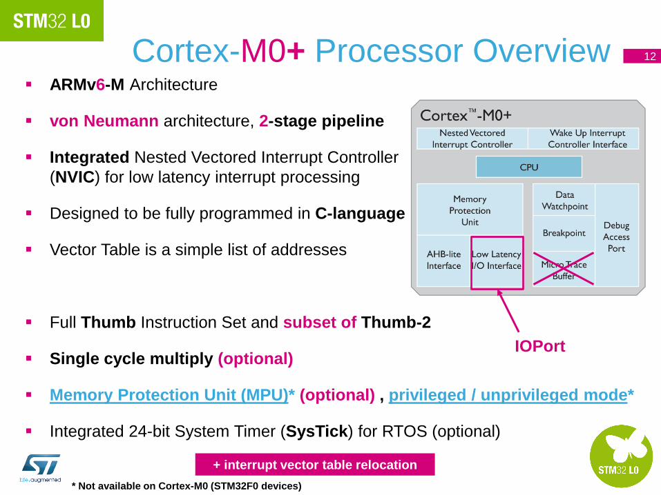
Cortex-M0+ Processor Overview ARMv6-M Architecture
von Neumann architecture, 2-stage pipeline
Integrated Nested Vectored Interrupt Controller
(NVIC) for low latency interrupt processing
Designed to be fully programmed in C-language
Vector Table is a simple list of addresses
Full Thumb Instruction Set and subset of Thumb-2
Single cycle multiply (optional)
Memory Protection Unit (MPU)* (optional) , privileged / unprivileged mode*
Integrated 24-bit System Timer (SysTick) for RTOS (optional)
12
IOPort
+ interrupt vector table relocation
* Not available on Cortex-M0 (STM32F0 devices)
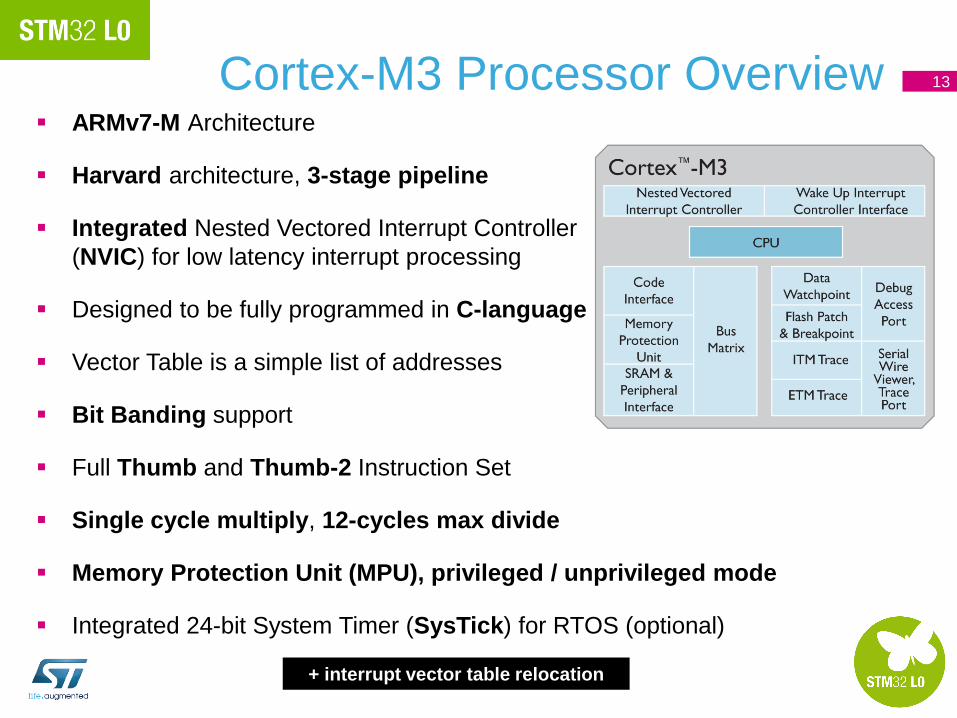
ARMv7-M Architecture
Harvard architecture, 3-stage pipeline
Integrated Nested Vectored Interrupt Controller
(NVIC) for low latency interrupt processing
Designed to be fully programmed in C-language
Vector Table is a simple list of addresses
Bit Banding support
Full Thumb and Thumb-2 Instruction Set
Single cycle multiply, 12-cycles max divide
Memory Protection Unit (MPU), privileged / unprivileged mode
Integrated 24-bit System Timer (SysTick) for RTOS (optional)
Cortex-M3 Processor Overview 13
+ interrupt vector table relocation
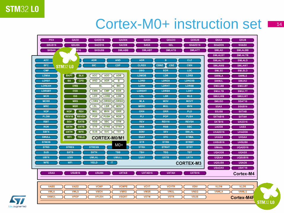
Cortex-M0+ instruction set 14
M0+

• Cortex M processors are FW and binary compatible
• Migrating path M0/M0+ >> M3 >> M4 is straight forward
• Instruction set of Cortex-Mx is strictly included in the instruction set of
Cortex-My (for x<y), allowing direct migration, while taking advantage
of higher MCU clock speed and von Neumann to Harvard
performance increase
• Re-compilation of the code is recommended
• from Cortex-M0/M0+ to Cortex-M3, in order to fully take
advantage of the higher performance ISA (e.g. HW division)
• From M0/M0+/M3 to M4 w/ FPU, in order to generate the FPU
code
• For a given STM32 family, a full peripheral set compatibility is
guaranteed in order to allow this simple migration path
15 Cortex-Mx – firmware compatibility (1/2)
Cortex-Mx – firmware compatibility (2/2)
• Cortex M processors are FW and binary compatible
• When moving from M0/M0+/M3 >> M4, some part of the code
might be re-coded using intrinsics, taking advantage of the
advanced DSP/SIMD instructions
• When moving backwards M3/M4 >> M0/M0+, the code needs to
be recompiled in order to use only M0 instruction codes
• Code density is equivalent on the different Cortex-M
implementations
• Code size differences for usual codes are bellow few percents,
provided that the same optimizations options are chosen in the
compiler
16
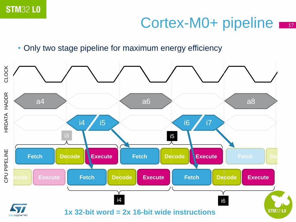
Decode Execute
Cortex-M0+ pipeline
• Only two stage pipeline for maximum energy efficiency
17
Fetch Decode Execute
Fetch Decode Execute
Fetch Decode Execute
Fetch Decode Execute
a4 a6 a8
Fetch Decode
HR
DA
TA
H
AD
DR
C
LO
CK
C
PU
PIP
EL
INE
i4 i5 i6 i7
1x 32-bit word = 2x 16-bit wide instructions
i3
i4
i5
i6

Cortex-M0+ Higher dynamic efficiency
• In pipelined processors, subsequent instructions are fetched while
executing current instructions
• In 2-stage pipeline: • Branch shadow is reduced and energy is saved!
• Branch turn-around is 1 cycle faster!
instructions fetched/decoded
but not used
3-stage
pipeline
18
2-stage
pipeline
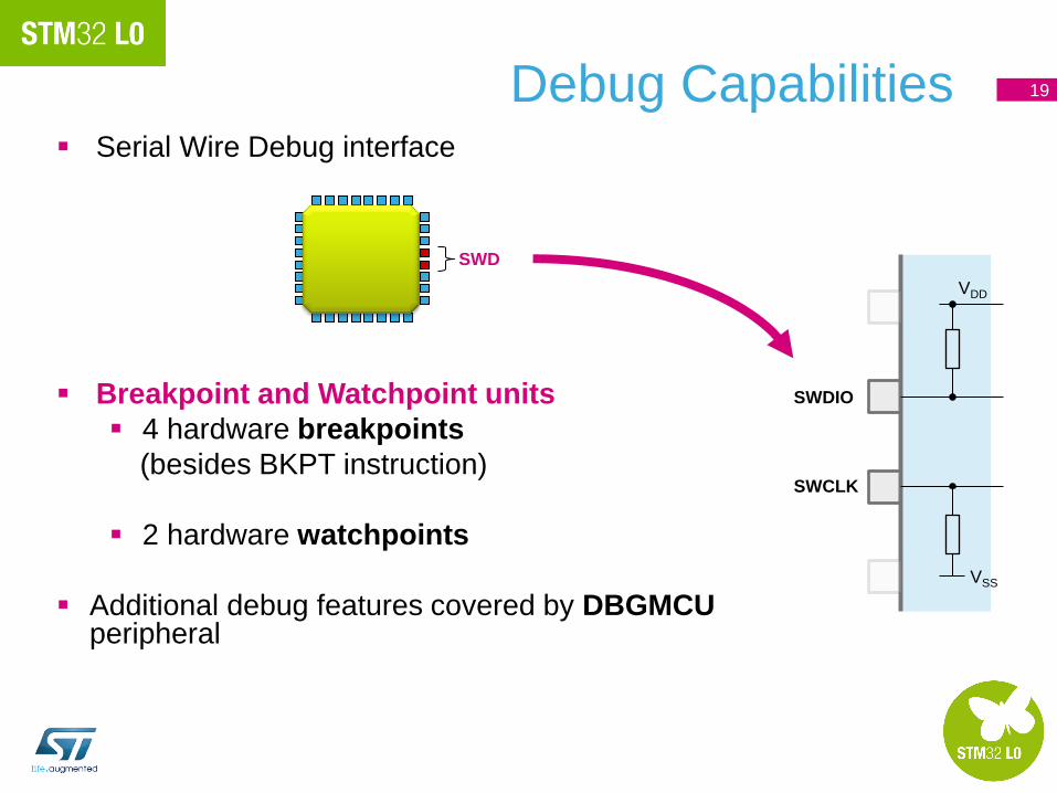
Serial Wire Debug interface
Breakpoint and Watchpoint units
4 hardware breakpoints
(besides BKPT instruction)
2 hardware watchpoints
Additional debug features covered by DBGMCU peripheral
Debug Capabilities
SWD
19
SWDIO
SWCLK
VDD
VSS
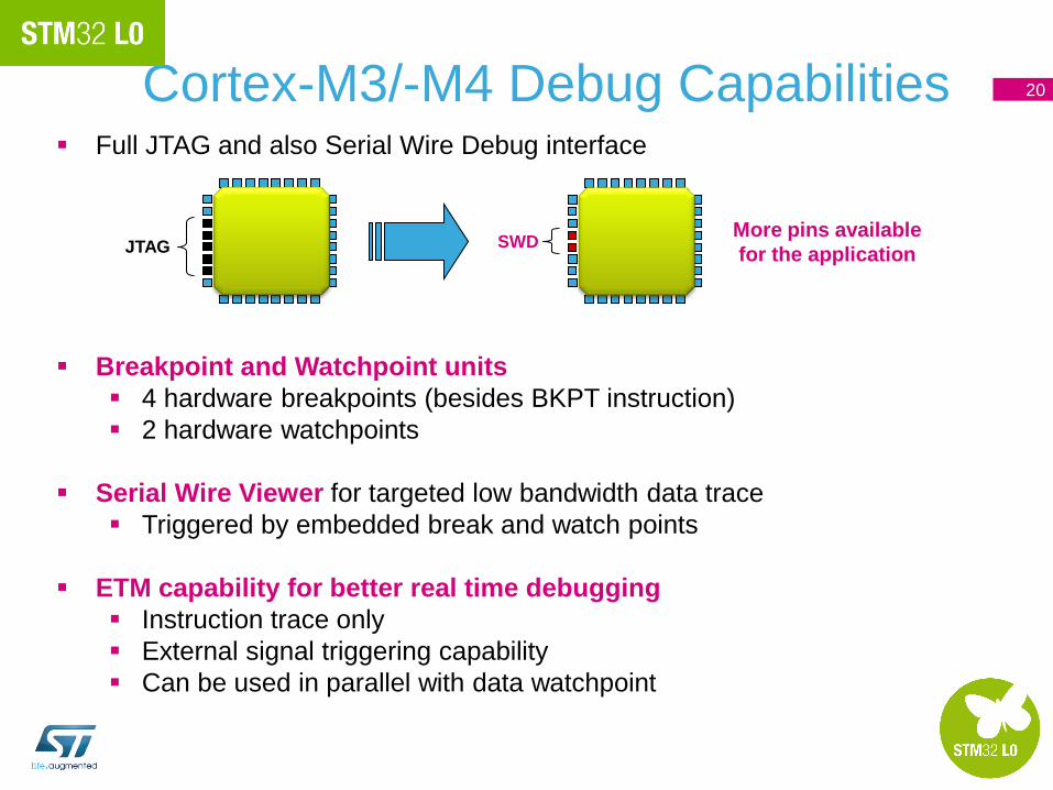
Full JTAG and also Serial Wire Debug interface
Breakpoint and Watchpoint units
4 hardware breakpoints (besides BKPT instruction)
2 hardware watchpoints
Serial Wire Viewer for targeted low bandwidth data trace
Triggered by embedded break and watch points
ETM capability for better real time debugging
Instruction trace only
External signal triggering capability
Can be used in parallel with data watchpoint
Cortex-M3/-M4 Debug Capabilities
JTAG SWD More pins available
for the application
20
Cortex-M0+ Architecture

Cortex-M0+ components
STM32 Cortex-M0+ implementation
Cortex-M0+ processor
Nested
Vectored
Interrupt
Controller
(NVIC)
Cortex-M0
processor
core
BUS MATRIX
DEBUG
Breakpoint
Unit (BPU)
+
Data
Watchpoint
Trigger (DWT)
Debugger
Interface
Debug Access
Port (DAP)
AHB-Lite interface
to system
Serial Wire
Debug (SWD)
IRQs
2-stage pipeline
(1)
SLEEP
SysTick
Timer
IO-Port
interface
(1)
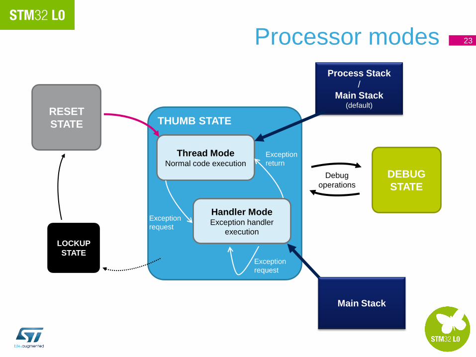
Processor modes 23
THUMB STATE
DEBUG
STATE
LOCKUP
STATE
Thread Mode Normal code execution
Exception
return
Exception
request
RESET
STATE
Debug
operations
Handler Mode Exception handler
execution
Exception
request
Process Stack
/
Main Stack (default)
Main Stack
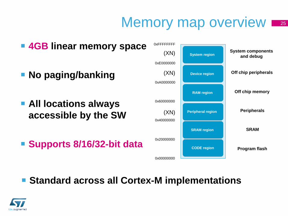
Memory map overview
4GB linear memory space
No paging/banking
All locations always
accessible by the SW
Supports 8/16/32-bit data
Standard across all Cortex-M implementations
0x00000000
0xFFFFFFFF
CODE region
SRAM region
0x20000000
0x40000000
Peripheral region
RAM region
Device region
0x60000000
0xA0000000
System region
0xE0000000
Program flash
SRAM
Peripherals
Off chip memory
Off chip peripherals
System components
and debug
25
(XN)
(XN)
(XN)
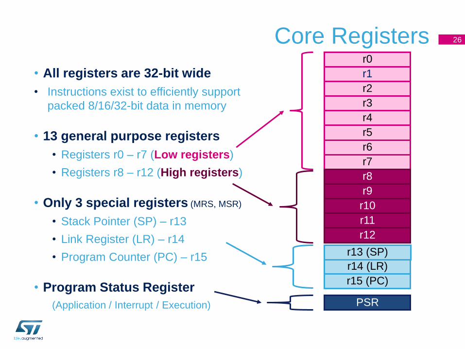
Core Registers
• All registers are 32-bit wide
• Instructions exist to efficiently support
packed 8/16/32-bit data in memory
• 13 general purpose registers
• Registers r0 – r7 (Low registers)
• Registers r8 – r12 (High registers)
• Only 3 special registers (MRS, MSR)
• Stack Pointer (SP) – r13
• Link Register (LR) – r14
• Program Counter (PC) – r15
• Program Status Register
(Application / Interrupt / Execution)
r0
r1
r2
r3
r4
r5
r6
r7
r8
r9
r10
r11
r12
r15 (PC)
r14 (LR)
PSR
r13 (SP)
26

r4
r15 (PC)
PSR
r13 (SP)
Register Usage Convention
• ARM Architecture Procedure Call Standard (AAPCS)
27
r0
r1
r2
r3
r5
r6
r7
r8
r9
r10
r11
r12
r14 (LR)
Non-Scratch
registers
Scratch registers
Arguments
to a callee
Local
variables
Return value
MOV R0,#4
BL FUNC
ADD R0,R0,#1
MOV R4,#4
BL FUNC
ADD R4,R4,#1
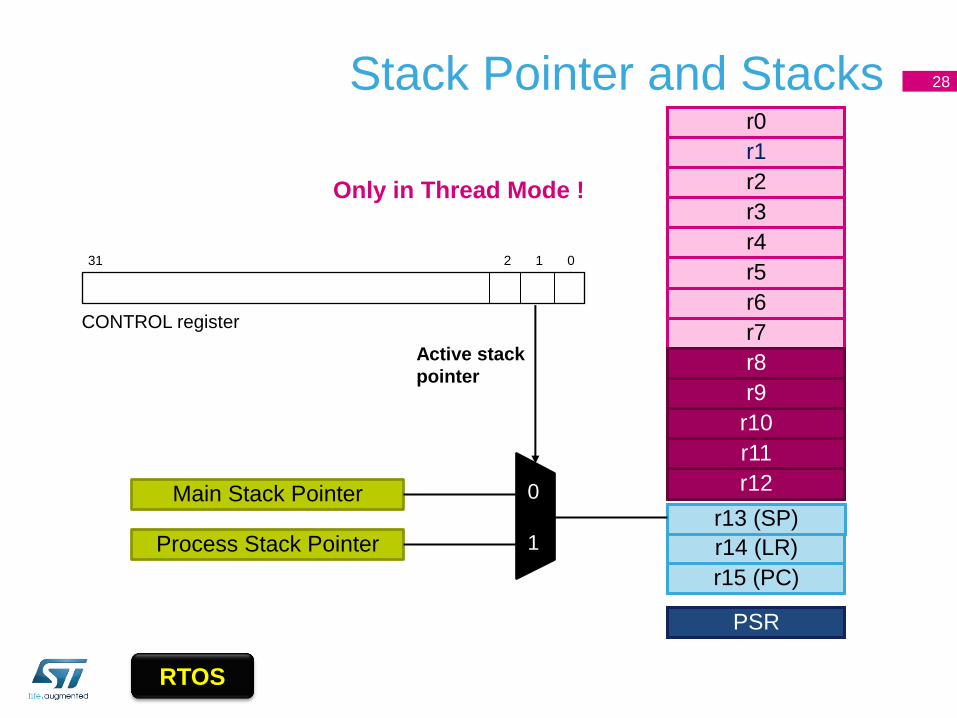
Stack Pointer and Stacks 28
r0
r1
r2
r3
r4
r5
r6
r7
r8
r9
r10
r11
r12
r15 (PC)
r14 (LR)
PSR
r13 (SP) Process Stack Pointer
Main Stack Pointer 0
1
CONTROL register
31 0 1 2
Active stack
pointer
Only in Thread Mode !
RTOS
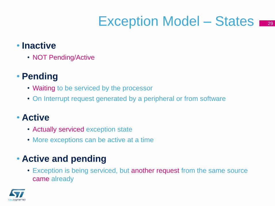
Exception Model – States
• Inactive
• NOT Pending/Active
• Pending
• Waiting to be serviced by the processor
• On Interrupt request generated by a peripheral or from software
• Active
• Actually serviced exception state
• More exceptions can be active at a time
• Active and pending
• Exception is being serviced, but another request from the same source
came already
29

Exception Model – Types and Priorities
No. Exception Type Priority Type of
Priority Descriptions
1 Reset -3 (Highest) fixed Reset
2 NMI -2 fixed Non-Maskable Interrupt
3 Hard Fault -1 fixed Default fault if other hander not
implemented
4-10 Reserved N.A. N.A.
11 SVCall Programmable settable Supervisor call (SVC)
12-13 Reserved N.A. N.A.
14 PendSV Programmable settable Request for System-Level Service
15 SYSTICK Programmable settable System Tick Timer
16 Interrupt #0 Programmable settable External Interrupt #0
…… ………………….. ……………….. settable …………………..
47 Interrupt#31 Programmable settable External Interrupt #31
30
4 priority levels
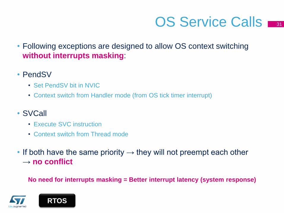
OS Service Calls
• Following exceptions are designed to allow OS context switching
without interrupts masking:
• PendSV
• Set PendSV bit in NVIC
• Context switch from Handler mode (from OS tick timer interrupt)
• SVCall
• Execute SVC instruction
• Context switch from Thread mode
• If both have the same priority → they will not preempt each other
→ no conflict
No need for interrupts masking = Better interrupt latency (system response)
31
RTOS
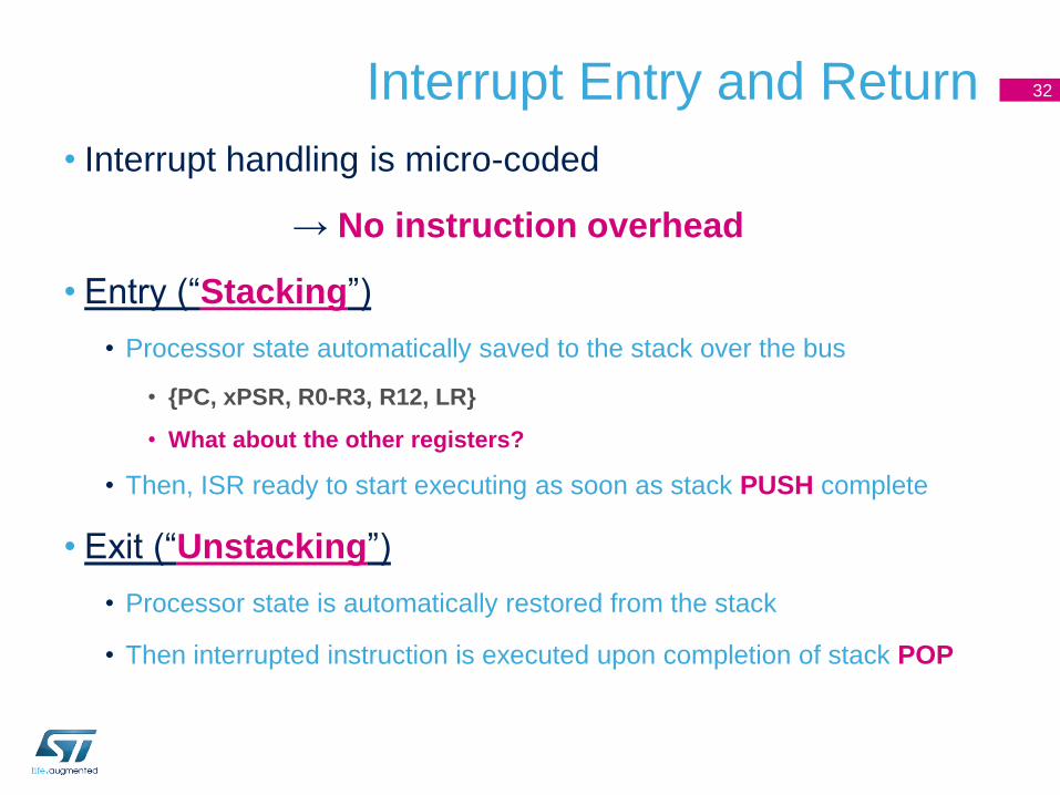
Interrupt Entry and Return
• Interrupt handling is micro-coded
→ No instruction overhead
• Entry (“Stacking”)
• Processor state automatically saved to the stack over the bus
• {PC, xPSR, R0-R3, R12, LR}
• What about the other registers?
• Then, ISR ready to start executing as soon as stack PUSH complete
• Exit (“Unstacking”)
• Processor state is automatically restored from the stack
• Then interrupted instruction is executed upon completion of stack POP
32

Preemption
• “Interruption of the exception handler”
• Depending on the priority
• If higher priority exception request comes while another
lower priority exception handler is executing
→ the higher priority exception can preempt the
lower priority exception handler
• Such exceptions are called nested exceptions
33
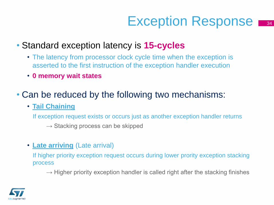
Exception Response
• Standard exception latency is 15-cycles
• The latency from processor clock cycle time when the exception is
asserted to the first instruction of the exception handler execution
• 0 memory wait states
• Can be reduced by the following two mechanisms:
• Tail Chaining
If exception request exists or occurs just as another exception handler returns
→ Stacking process can be skipped
• Late arriving (Late arrival)
If higher priority exception request occurs during lower prority exception stacking
process
→ Higher priority exception handler is called right after the stacking finishes
34
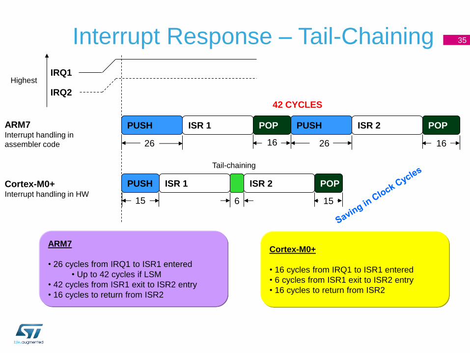
PUSH POP ISR 1 PUSH POP ISR 2
PUSH ISR 1 POP ISR 2
26 16 26 16
15
IRQ1
IRQ2
ARM7 Interrupt handling in
assembler code
Cortex-M0+ Interrupt handling in HW
15
42 CYCLES
Highest
Tail-chaining
ARM7
• 26 cycles from IRQ1 to ISR1 entered
• Up to 42 cycles if LSM
• 42 cycles from ISR1 exit to ISR2 entry
• 16 cycles to return from ISR2
Cortex-M0+
• 16 cycles from IRQ1 to ISR1 entered
• 6 cycles from ISR1 exit to ISR2 entry
• 16 cycles to return from ISR2
6
35 Interrupt Response – Tail-Chaining
ISR 2
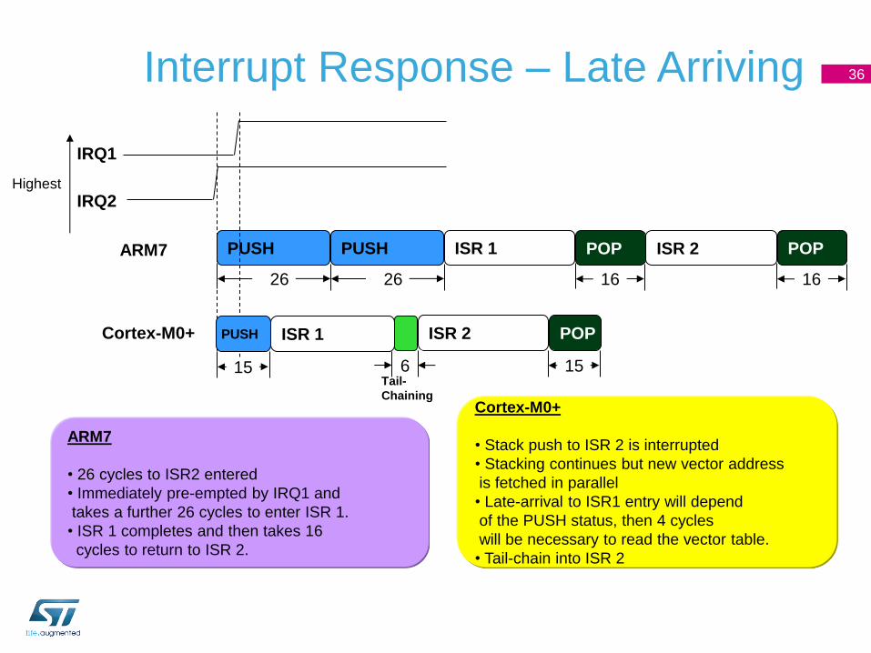
Interrupt Response – Late Arriving
IRQ1
IRQ2
ISR 2
Tail-
Chaining
ISR 1 PUSH PUSH POP POP
PUSH POP
ARM7
Cortex-M0+
Highest
Cortex-M0+
• Stack push to ISR 2 is interrupted
• Stacking continues but new vector address
is fetched in parallel
• Late-arrival to ISR1 entry will depend
of the PUSH status, then 4 cycles
will be necessary to read the vector table.
• Tail-chain into ISR 2
ARM7
• 26 cycles to ISR2 entered
• Immediately pre-empted by IRQ1 and
takes a further 26 cycles to enter ISR 1.
• ISR 1 completes and then takes 16
cycles to return to ISR 2.
26 16 16 26
15 6
ISR 1
15
36
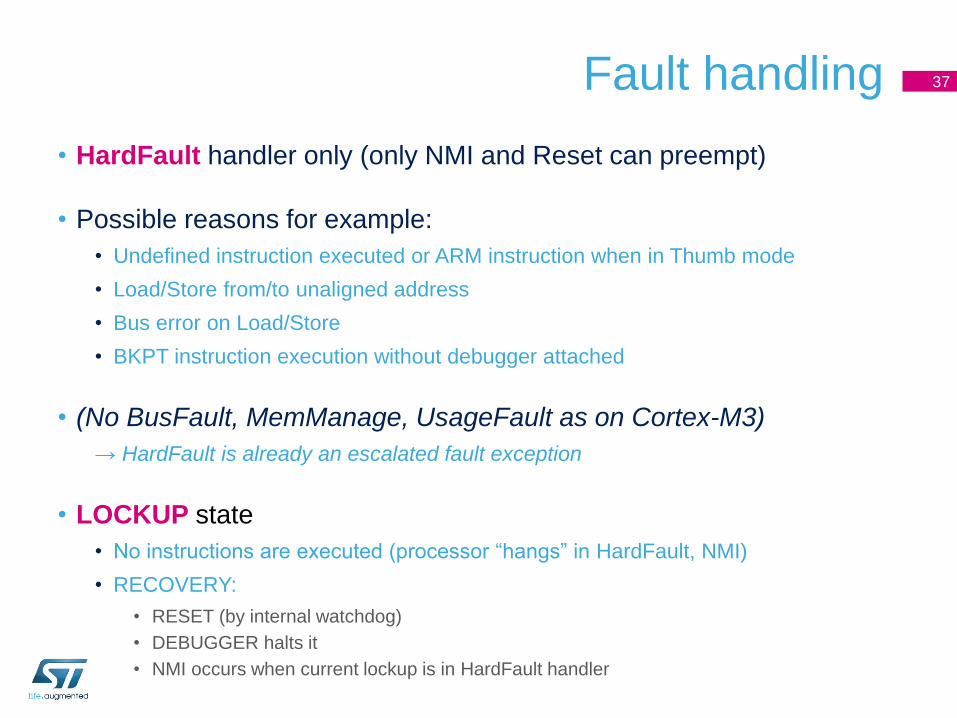
Fault handling
• HardFault handler only (only NMI and Reset can preempt)
• Possible reasons for example:
• Undefined instruction executed or ARM instruction when in Thumb mode
• Load/Store from/to unaligned address
• Bus error on Load/Store
• BKPT instruction execution without debugger attached
• (No BusFault, MemManage, UsageFault as on Cortex-M3)
→ HardFault is already an escalated fault exception
• LOCKUP state
• No instructions are executed (processor “hangs” in HardFault, NMI)
• RECOVERY:
• RESET (by internal watchdog)
• DEBUGGER halts it
• NMI occurs when current lockup is in HardFault handler
37
Cortex-M0+ Instruction Set
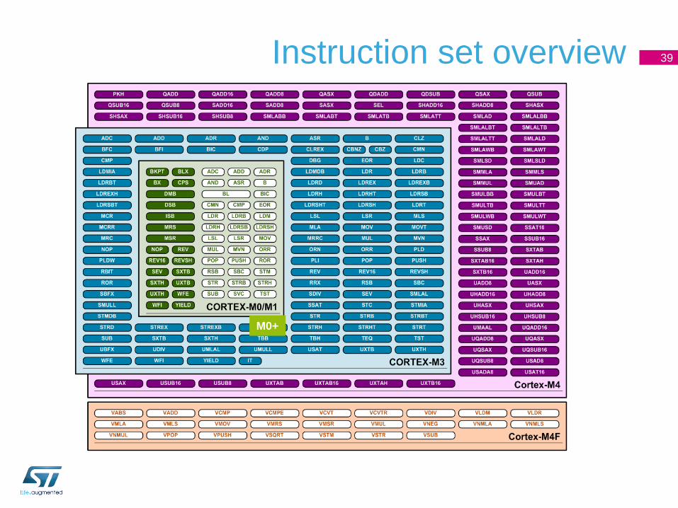
Instruction set overview 39
M0+
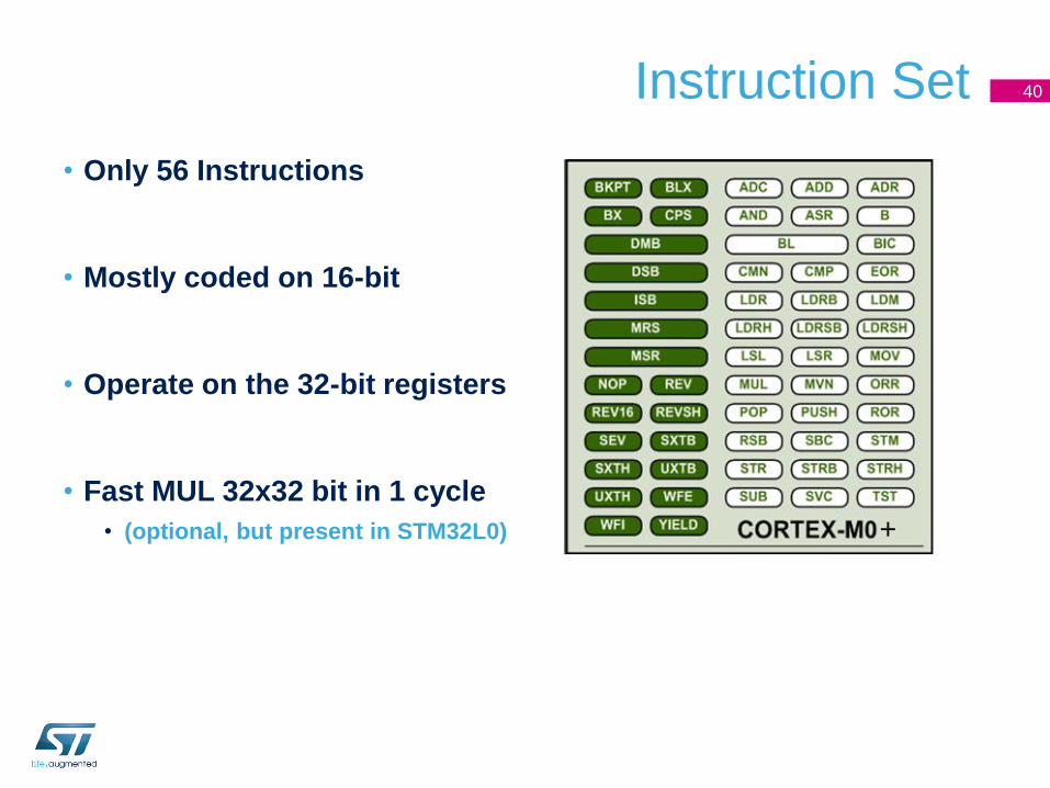
Instruction Set
• Only 56 Instructions
• Mostly coded on 16-bit
• Operate on the 32-bit registers
• Fast MUL 32x32 bit in 1 cycle
• (optional, but present in STM32L0)
40
+

Cortex-M0 instruction set – closer look
• ARM-v6M Architecture : Only 56 Instructions
• 46 instructions (generally generated by a C compiler)
• 10 instructions for System & special usage
• 8/16/32-bits data transfers possible on One Instruction
• No Hardware Divide
• No IT ( If-Then-Else) blocks to avoid small Branches
• All instructions are 16-bits Thumb to save code memory,
except the 32-bit Thumb-2 instructions BL, DMB,
DSB, ISB, MRS and MSR.
• Load/Store instructions takes 2 cycles each
• Most of MOV, ADD, SUBTRACT, Compare, Logical, SHIFT instructions take 1
cycle
• Branches takes from 1 to 4 cycles ( depends if conditional, not or with link)
• “MULS” instruction provides a 32-bit x 32-bit multiply that yields the least significant
32-bits with 1 cycle Operation
41

System blocks
Internal Memories
50
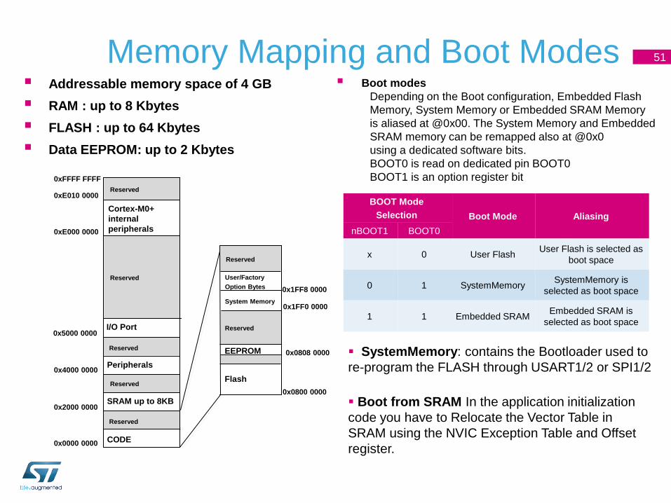
Memory Mapping and Boot Modes 51
BOOT Mode
Selection Boot Mode Aliasing
nBOOT1 BOOT0
x 0 User Flash User Flash is selected as
boot space
0 1 SystemMemory SystemMemory is
selected as boot space
1 1 Embedded SRAM Embedded SRAM is
selected as boot space
Boot modes
Depending on the Boot configuration, Embedded Flash
Memory, System Memory or Embedded SRAM Memory
is aliased at @0x00. The System Memory and Embedded
SRAM memory can be remapped also at @0x0
using a dedicated software bits.
BOOT0 is read on dedicated pin BOOT0
BOOT1 is an option register bit
Addressable memory space of 4 GB
RAM : up to 8 Kbytes
FLASH : up to 64 Kbytes
Data EEPROM: up to 2 Kbytes
SystemMemory: contains the Bootloader used to
re-program the FLASH through USART1/2 or SPI1/2
Boot from SRAM In the application initialization
code you have to Relocate the Vector Table in
SRAM using the NVIC Exception Table and Offset
register.
CODE
SRAM up to 8KB
Peripherals
0x0000 0000
0x2000 0000
0x4000 0000
0xE010 0000
0xFFFF FFFF
Reserved
Reserved
System Memory
Reserved
User/Factory
Option Bytes
Cortex-M0+
internal
peripherals 0xE000 0000
Reserved
Reserved 0x5000 0000
Flash
I/O Port
Reserved
Reserved
EEPROM
0x0800 0000
0x0808 0000
0x1FF8 0000
0x1FF0 0000
Flash Operations: Program memory
• The Flash program memory write and erase operations:
• After reset the Program memory is protected, an unlocking sequence should be
performed (write of 2 key values on PEKEYR and write 2 key values on
PRGKEYR) to unlock the Program memory
• The Flash can be programmed by word or by half page with 64 Bytes at a time (half
page programming can be done only from RAM, or DMA).
• Flash can be erased page-wise
• Access to NVM is stalled during program\erase
• The FLASH can be in Power Down mode when system is in RUN or
LP RUN (CPU is executing from RAM) or in SLEEP mode.
52
NVM Operations: Data EEPROM memory
• The data EEPROM memory write and erase operations :
• After reset the Data memory is protected, an unlocking sequence should be
performed (write of 2 key values on PEKEYR register) to unlock the Data memory
• Data memory can be erased by word
• The data memory can be programmed with:
• Word (32-bit) / Half Word (16-bit) / Byte (8-bit)
• Fast Word / Half Word / Byte write: The Fast data memory programming
operations are used when the memory is erased before. The FIX bit (Fixed
time data write) must be cleared= 0. The Fast programming operation takes
only 1*tPROG ( programming time).
• Word / Half Word / Byte write: no need for erase before, the word to be
written will be automatically erased. The programming operation takes 1 or
2*tPROG ( programming time)., The programming time can stick to 2*tPROG
with FIX (Fixed time data write) bit set.
53
Information Block
• The Information Block consists of:
• 4 KBytes for SystemMemory : contains embedded Bootloader
• 4*8 Bytes for User Option bytes (complemented for security)
• 96 Byte for Factory Option Byte (read only)
• option bytes configure the product :
• 1 for 16 sectors (4KByte each) write protection and sector read out protection
• 1 for global read out protection and selection of Write or sector readout protection
• 1 for Device configuration:
• Brown Out Reset Level • Independent WatchDoG HW/SW mode • Reset when entering STANDBY mode • Reset when entering STOP mode • Boot1
• After unlocking the NVM (write 2 key values on PEKEYR), the user has to authorize the Option byte programming by writing 2 key values on OPTKEYR register then he can program the Option bytes
• On POR reset, the option bytes loader performs a read of the information block and stores the data into the FLASH registers (when programmed the option bytes are taken into account only after POR reset). User can use the OBL_Launch bit to initiate the option bytes loader (generating SYSTEM reset).
54
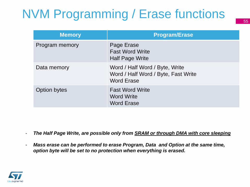
NVM Programming / Erase functions 55
Memory Program/Erase
Program memory Page Erase
Fast Word Write
Half Page Write
Data memory
Word / Half Word / Byte, Write
Word / Half Word / Byte, Fast Write
Word Erase
Option bytes
Fast Word Write
Word Write
Word Erase
- The Half Page Write, are possible only from SRAM or through DMA with core sleeping
- Mass erase can be performed to erase Program, Data and Option at the same time,
option byte will be set to no protection when everything is erased.
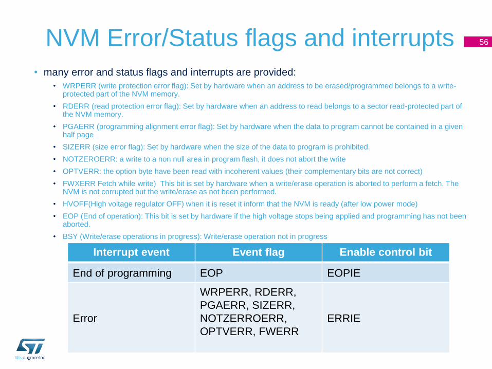
NVM Error/Status flags and interrupts
• many error and status flags and interrupts are provided:
• WRPERR (write protection error flag): Set by hardware when an address to be erased/programmed belongs to a write-protected part of the NVM memory.
• RDERR (read protection error flag): Set by hardware when an address to read belongs to a sector read-protected part of the NVM memory.
• PGAERR (programming alignment error flag): Set by hardware when the data to program cannot be contained in a given half page
• SIZERR (size error flag): Set by hardware when the size of the data to program is prohibited.
• NOTZEROERR: a write to a non null area in program flash, it does not abort the write
• OPTVERR: the option byte have been read with incoherent values (their complementary bits are not correct)
• FWXERR Fetch while write) This bit is set by hardware when a write/erase operation is aborted to perform a fetch. The NVM is not corrupted but the write/erase as not been performed.
• HVOFF(High voltage regulator OFF) when it is reset it inform that the NVM is ready (after low power mode)
• EOP (End of operation): This bit is set by hardware if the high voltage stops being applied and programming has not been aborted.
• BSY (Write/erase operations in progress): Write/erase operation not in progress
56
Interrupt event Event flag Enable control bit
End of programming EOP EOPIE
Error
WRPERR, RDERR,
PGAERR, SIZERR,
NOTZERROERR,
OPTVERR, FWERR
ERRIE
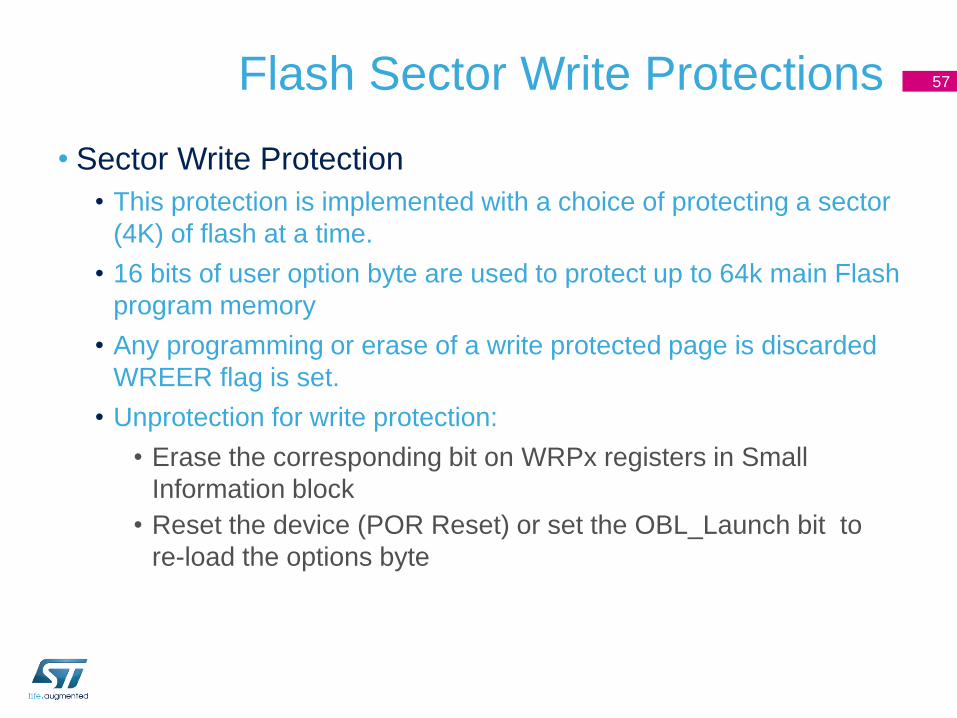
Flash Sector Write Protections
• Sector Write Protection
• This protection is implemented with a choice of protecting a sector
(4K) of flash at a time.
• 16 bits of user option byte are used to protect up to 64k main Flash
program memory
• Any programming or erase of a write protected page is discarded
WREER flag is set.
• Unprotection for write protection:
• Erase the corresponding bit on WRPx registers in Small
Information block
• Reset the device (POR Reset) or set the OBL_Launch bit to
re-load the options byte
57
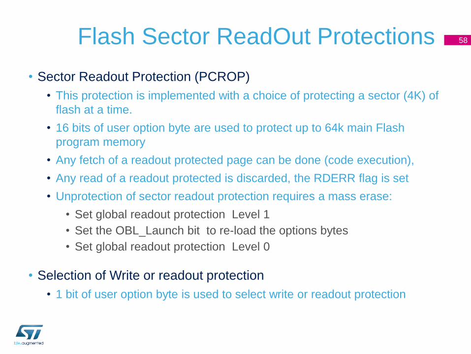
Flash Sector ReadOut Protections
• Sector Readout Protection (PCROP)
• This protection is implemented with a choice of protecting a sector (4K) of
flash at a time.
• 16 bits of user option byte are used to protect up to 64k main Flash
program memory
• Any fetch of a readout protected page can be done (code execution),
• Any read of a readout protected is discarded, the RDERR flag is set
• Unprotection of sector readout protection requires a mass erase:
• Set global readout protection Level 1
• Set the OBL_Launch bit to re-load the options bytes
• Set global readout protection Level 0
• Selection of Write or readout protection
• 1 bit of user option byte is used to select write or readout protection
58
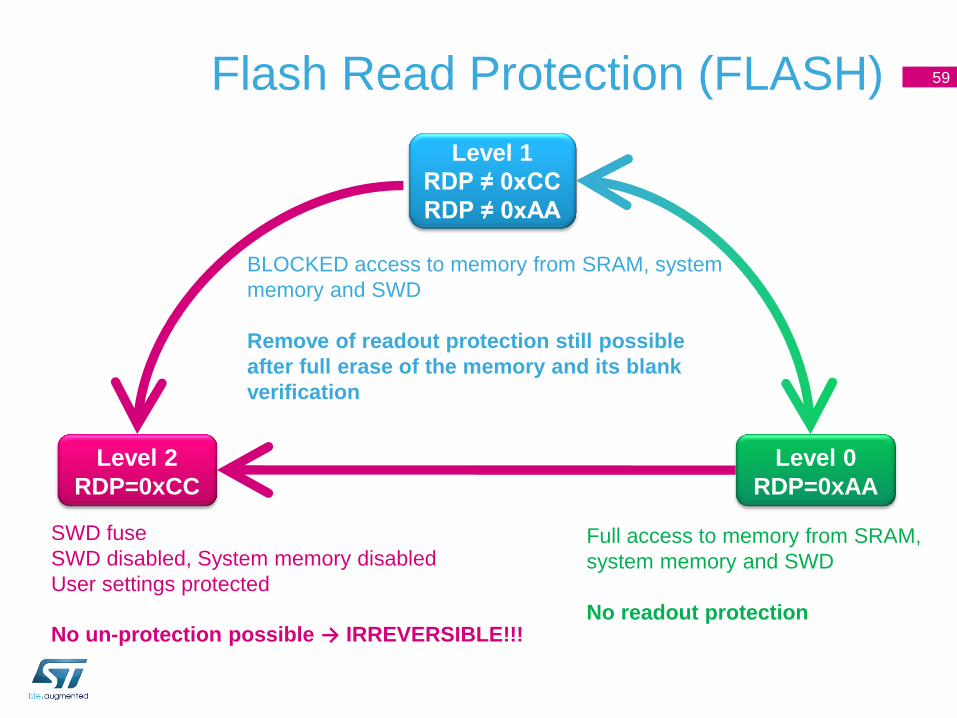
Flash Read Protection (FLASH)
Level 2
RDP=0xCC
Level 0
RDP=0xAA
Level 1
RDP ≠ 0xCC
RDP ≠ 0xAA
SWD fuse
SWD disabled, System memory disabled
User settings protected
No un-protection possible → IRREVERSIBLE!!!
Full access to memory from SRAM,
system memory and SWD
No readout protection
BLOCKED access to memory from SRAM, system
memory and SWD
Remove of readout protection still possible
after full erase of the memory and its blank
verification
59
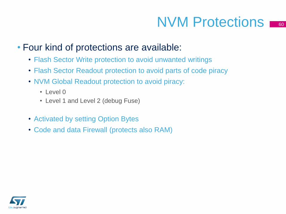
NVM Protections
• Four kind of protections are available:
• Flash Sector Write protection to avoid unwanted writings
• Flash Sector Readout protection to avoid parts of code piracy
• NVM Global Readout protection to avoid piracy:
• Level 0
• Level 1 and Level 2 (debug Fuse)
• Activated by setting Option Bytes
• Code and data Firewall (protects also RAM)
60
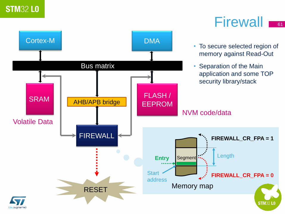
Firewall 61
Cortex-M DMA
Bus matrix
SRAM FLASH /
EEPROM AHB/APB bridge
FIREWALL
Volatile Data
NVM code/data
RESET
• To secure selected region of
memory against Read-Out
• Separation of the Main
application and some TOP
security library/stack
Memory map
Start
address
Length Segment
FIREWALL_CR_FPA = 0
FIREWALL_CR_FPA = 1
Entry
System blocks
Reset and Clock Control (RCC)
62
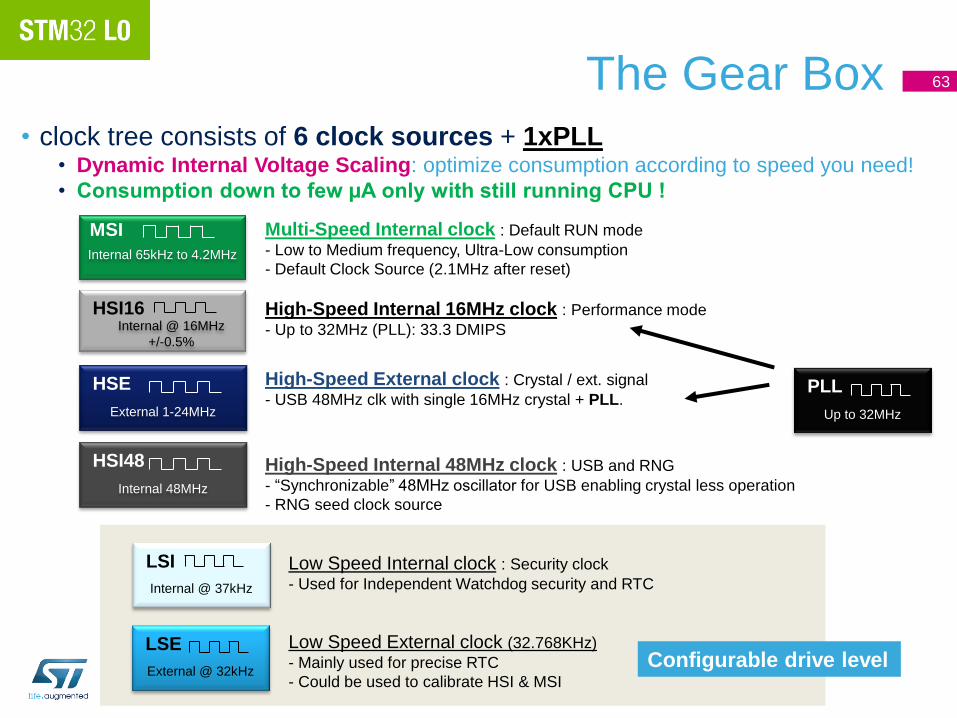
The Gear Box • clock tree consists of 6 clock sources + 1xPLL
• Dynamic Internal Voltage Scaling: optimize consumption according to speed you need!
• Consumption down to few µA only with still running CPU !
63
High-Speed Internal 16MHz clock : Performance mode
- Up to 32MHz (PLL): 33.3 DMIPS
Multi-Speed Internal clock : Default RUN mode
- Low to Medium frequency, Ultra-Low consumption
- Default Clock Source (2.1MHz after reset)
Low Speed Internal clock : Security clock
- Used for Independent Watchdog security and RTC
High-Speed External clock : Crystal / ext. signal
- USB 48MHz clk with single 16MHz crystal + PLL.
Low Speed External clock (32.768KHz)
- Mainly used for precise RTC
- Could be used to calibrate HSI & MSI
HSI16 Internal @ 16MHz
+/-0.5%
MSI
Internal 65kHz to 4.2MHz
LSI
Internal @ 37kHz
HSE
External 1-24MHz
LSE
External @ 32kHz
PLL
Up to 32MHz
HSI48
Internal 48MHz
High-Speed Internal 48MHz clock : USB and RNG
- “Synchronizable” 48MHz oscillator for USB enabling crystal less operation
- RNG seed clock source
Configurable drive level

Clock controller: the “Gearbox”
CSS
HSE Osc
OSC_OUT
OSC_IN
1 -24
MHz
up to 32
MHz
SYSCLK x3...x48,
/2,/3,/4 PLL PLLCLK
HSI RC 16MHz
MSI RC
64KHz, …, 4.2 MHz
ADCCLK
SYSCLK
HSI
HSE
PLLCLK
MCO /1,/2,/4,/8,/
16
MSI
LSE
LSI
LSI RC
32.768KHz
/2, 4,
8,16
LSE OSc
OSC32_IN
OSC32_OUT
~37KHz IWDGCLK
RTCCLK
LCDCLK
Low speed path: for low
consumption while CPU is static
Medium speed path: for low
consumption while CPU is at low
frequency
High speed path: for performance
capable to scale to the desired level
frequency (PLL)- change on the fly of
frequency
64
CSS
HSI48 RC
CRS
USBCLK
RBGCLK
48MHz
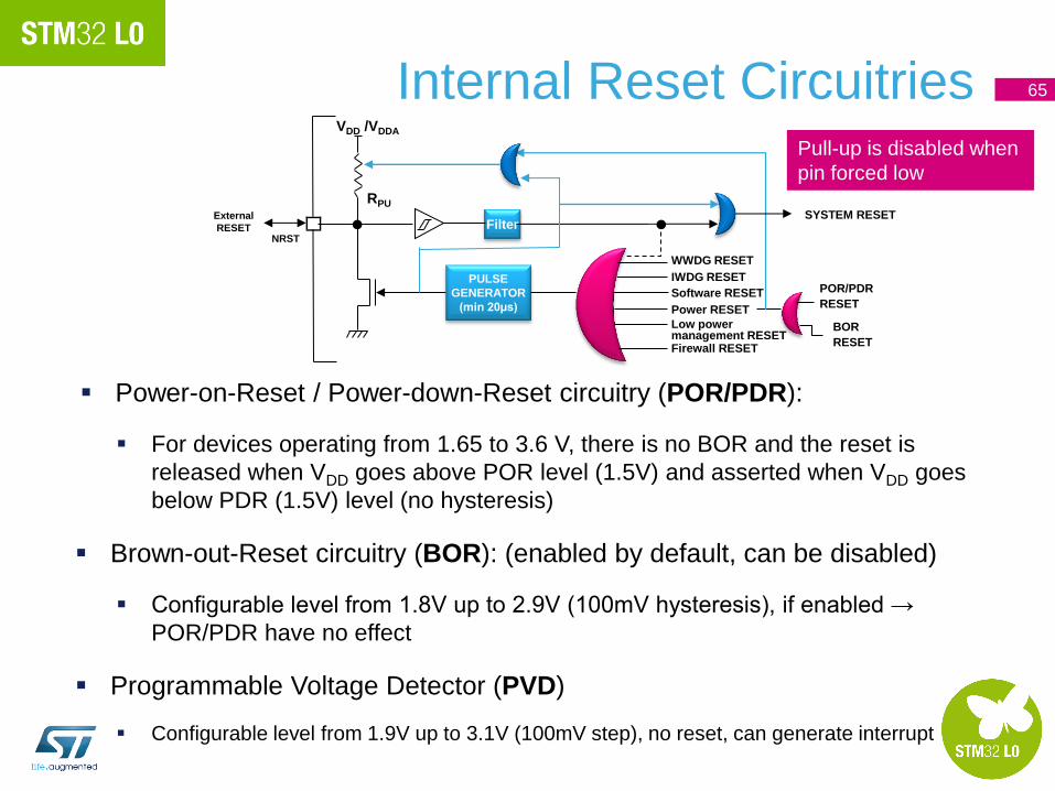
Internal Reset Circuitries
Power-on-Reset / Power-down-Reset circuitry (POR/PDR):
For devices operating from 1.65 to 3.6 V, there is no BOR and the reset is
released when VDD goes above POR level (1.5V) and asserted when VDD goes
below PDR (1.5V) level (no hysteresis)
Brown-out-Reset circuitry (BOR): (enabled by default, can be disabled)
Configurable level from 1.8V up to 2.9V (100mV hysteresis), if enabled →
POR/PDR have no effect
Programmable Voltage Detector (PVD)
Configurable level from 1.9V up to 3.1V (100mV step), no reset, can generate interrupt
65
Filter
VDD /VDDA
RPU
PULSE
GENERATOR
(min 20µs)
SYSTEM RESET
NRST
WWDG RESET
IWDG RESET
Software RESET
Power RESET
Low power management RESET
External
RESET
BOR
RESET
POR/PDR
RESET
Firewall RESET
Pull-up is disabled when
pin forced low
System blocks
GPIO
66
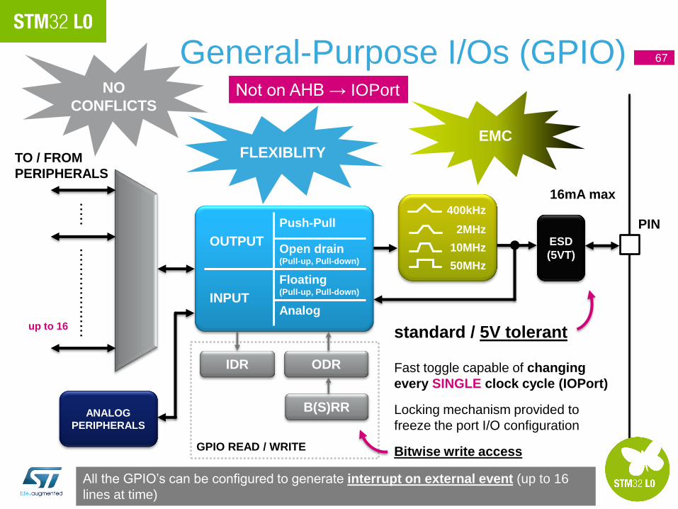
NO
CONFLICTS
General-Purpose I/Os (GPIO) 67
OUTPUT
Push-Pull
Open drain (Pull-up, Pull-down)
INPUT
Floating (Pull-up, Pull-down)
Analog
400kHz
2MHz
10MHz
50MHz
................... .....
TO / FROM
PERIPHERALS
PIN
ANALOG
PERIPHERALS
IDR ODR
B(S)RR
up to 16 standard / 5V tolerant
ESD
(5VT)
Fast toggle capable of changing
every SINGLE clock cycle (IOPort)
Locking mechanism provided to
freeze the port I/O configuration
Bitwise write access
GPIO READ / WRITE
16mA max
All the GPIO’s can be configured to generate interrupt on external event (up to 16
lines at time)
Not on AHB → IOPort
FLEXIBLITY EMC
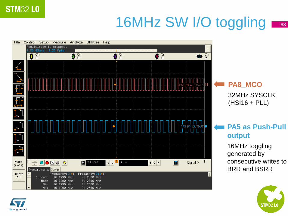
16MHz SW I/O toggling 68
PA8_MCO
32MHz SYSCLK
(HSI16 + PLL)
PA5 as Push-Pull
output
16MHz toggling
generated by
consecutive writes to
BRR and BSRR
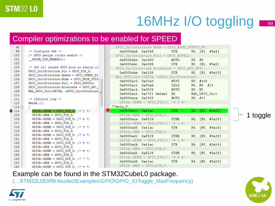
16MHz I/O toggling Compiler optimizations to be enabled for SPEED
69
1 toggle
Example can be found in the STM32CubeL0 package. (…STM32L053R8-Nucleo\Examples\GPIO\GPIO_IOToggle_MaxFrequency)
GPIOs in numbers
• Up to 51 multifunction bi-directional I/O ports available: 83% IO ratio
• Up to 44 I/Os are 5V Tolerant
• Up to 16 lines out of 51 GPIOs can be set-up for external interrupt at a time
• Ultralow leakage per I/O: 50nA (maximum @ max temperature)
• Maximal achievable I/O SW toggling speed: 16MHz
• Maximal I/O frequency: 50MHz
70
70
GPIO Configuration Modes
(1) VDD_FT is a potential specific to five-volt tolerant I/Os and different from VDD.
To On-chip Peripherals
Analog
From On-chip Peripherals
Push-Pull
Open Drain Output Driver
I/O
pin
VSS
On/Off
Pu
ll -
Up
P
ull -
Do
wn
VDD
On/Off
Bit
Se
t/R
es
et
Re
gis
ter
Inp
ut
Data
Reg
iste
r O
utp
ut
Data
Reg
iste
r
Read / Write
Alternate Function Input
Alternate Function Output
Schmitt
Trigger
VDD
VSS
0
Input Driver
Read
Write
On Off
VDD or VDD_FT(1)
VSS
OUTPUT
CONTROL
Analog
MODER(i)
[1:0]
OTYPER(i)
[1:0] I/O configuration
PUPDR(i)
[1:0]
11 x Analog mode x
01
0
0 0 Output Open Drain
0 1 Output Open Drain with Pull-up
1 0 Output Open Drain with Pull-down 1
0 0 Output Push Pull
0 1 Output Push Pull with Pull-up
1 0 Output Push Pull with Pull-down
10
0
1 0 0 Alternate Function Open Drain
0 1 Alternate Function OD Pull-up
1 0 Alternate Function OD Pull-down
0 0 Alternate Function Push Pull
0 1 Alternate Function PP Pull-up
1 0 Alternate Function PP Pull-down
00 x 0 0 Input floating
0 1 Input with Pull-up
1 0 Input with Pull-down
* In output mode, the I/O speed is configurable through OSPEEDR register:
2MHz, 10MHz or 50MHz
71
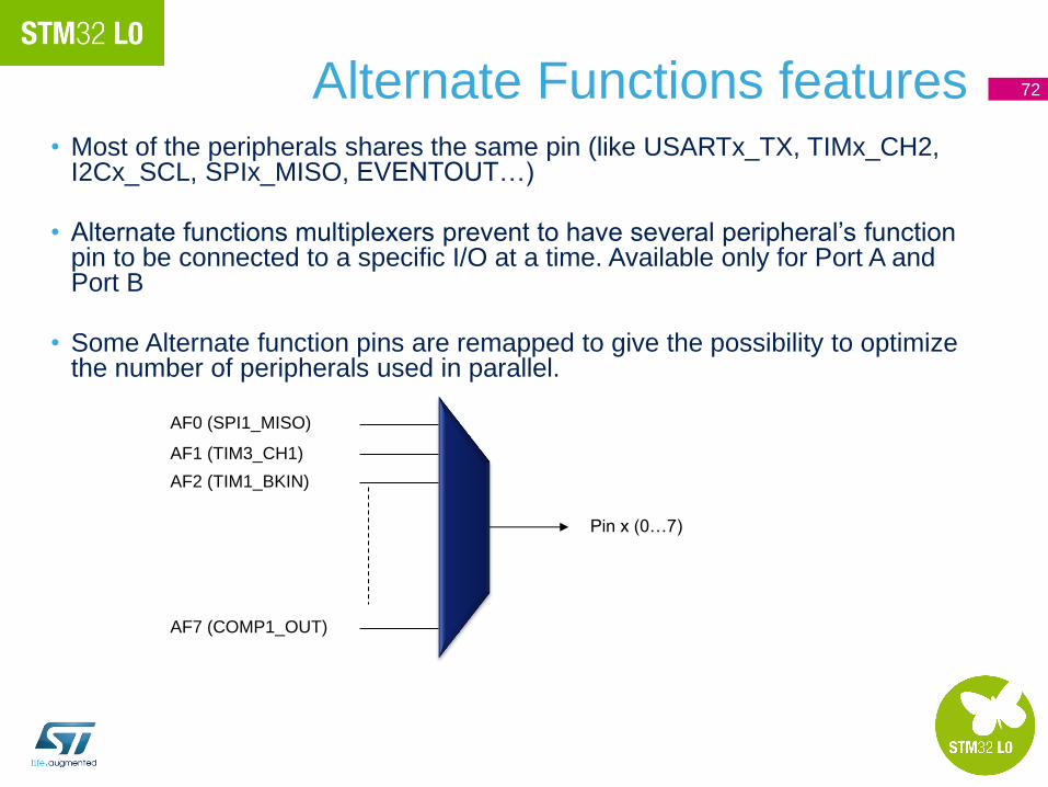
Alternate Functions features • Most of the peripherals shares the same pin (like USARTx_TX, TIMx_CH2,
I2Cx_SCL, SPIx_MISO, EVENTOUT…)
• Alternate functions multiplexers prevent to have several peripheral’s function pin to be connected to a specific I/O at a time. Available only for Port A and Port B
• Some Alternate function pins are remapped to give the possibility to optimize the number of peripherals used in parallel.
AF0 (SPI1_MISO)
AF1 (TIM3_CH1)
AF2 (TIM1_BKIN)
AF7 (COMP1_OUT)
Pin x (0…7)
72

Atomic operations - BSRR and BRR
• Very often we need fast and atomic access to GPIO pins
• To avoid any read + modify + write access
• Multiple bit modification at the same time in one operation
• Write only
73
BR15 BR0 BS15 BS0
Write 1 means bit RESET
in the ODR Write 1 means bit SET
in the ODR
• With a correct combination you may set and reset any number of pins at the same time (one CPU write)
• All other pins (where 0 was written) remain unchanged.
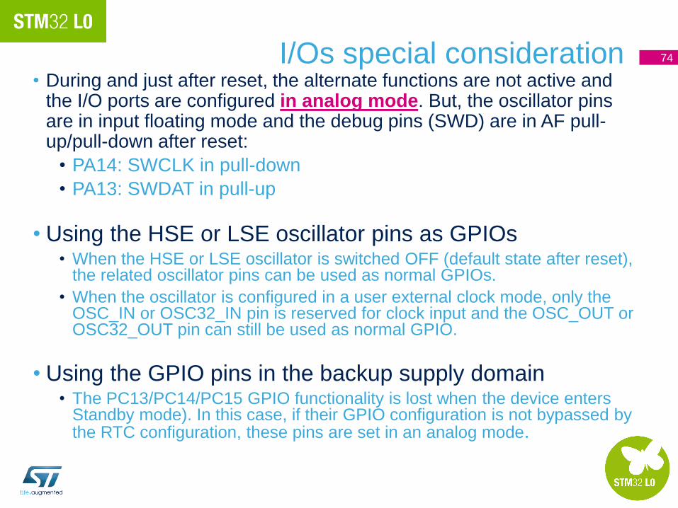
I/Os special consideration • During and just after reset, the alternate functions are not active and
the I/O ports are configured in analog mode. But, the oscillator pins are in input floating mode and the debug pins (SWD) are in AF pull-up/pull-down after reset:
• PA14: SWCLK in pull-down
• PA13: SWDAT in pull-up
• Using the HSE or LSE oscillator pins as GPIOs • When the HSE or LSE oscillator is switched OFF (default state after reset),
the related oscillator pins can be used as normal GPIOs.
• When the oscillator is configured in a user external clock mode, only the OSC_IN or OSC32_IN pin is reserved for clock input and the OSC_OUT or OSC32_OUT pin can still be used as normal GPIO.
• Using the GPIO pins in the backup supply domain • The PC13/PC14/PC15 GPIO functionality is lost when the device enters
Standby mode). In this case, if their GPIO configuration is not bypassed by the RTC configuration, these pins are set in an analog mode.
74
System blocks
Extended Interrupts/Events
Controller (EXTI)
75

Extended Interrupts/Events Contr. (EXTI)
• external and internal asynchronous events / interrupts
• External configurable lines can be mapped to the I/Os (up to 16 at a time)
• Internal lines are sensing output signals of some asynchronous internal peripherals
• Configurable – the same as the external line but sensing internal signal
• Direct – no configuration needed, always active if the peripheral is running and System is put in given Mode
• Can generate interrupt request and Wake-Up the MCU from almost any low-power mode
76
Interrupt Request
Appropriate
System Mode
Direct line
Each configurable
line has its own
edge detector
Internal configurable line
(e.g. Comparator output)
External
configurable line
(I/O pin) Event
signal
Wake-Up
signal
Interrupt Mask
Register
Pending Request
Register
Software Interrupt
Event Register
Rising Trigger
Selection Reg.
Falling Trigger
Selection Reg.
Event Mask
Register
1 2 3
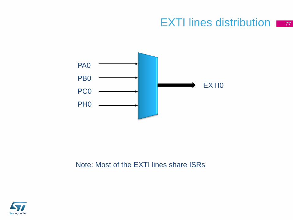
EXTI lines distribution 77
PA0
PB0
PC0
PH0
EXTI0
Note: Most of the EXTI lines share ISRs
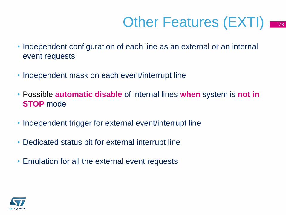
Other Features (EXTI)
• Independent configuration of each line as an external or an internal
event requests
• Independent mask on each event/interrupt line
• Possible automatic disable of internal lines when system is not in
STOP mode
• Independent trigger for external event/interrupt line
• Dedicated status bit for external interrupt line
• Emulation for all the external event requests
78
STM32L0 Low-Power Modes
OBJECTIVES
• Remind ARM Cortex-Mx Low-Power modes architecture
• Introduce STM32L0 Low-Power modes implementation
• Discuss the differences and possible application
• Check the consumption (exercises)
81
After this part of presentation you will know
the differences and capabilities of STM32L0
Low-Power modes.

Low-Power Modes
ARM Cortex-Mx Support
82
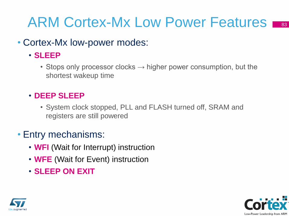
ARM Cortex-Mx Low Power Features
• Cortex-Mx low-power modes:
• SLEEP
• Stops only processor clocks → higher power consumption, but the
shortest wakeup time
• DEEP SLEEP
• System clock stopped, PLL and FLASH turned off, SRAM and
registers are still powered
• Entry mechanisms:
• WFI (Wait for Interrupt) instruction
• WFE (Wait for Event) instruction
• SLEEP ON EXIT
83
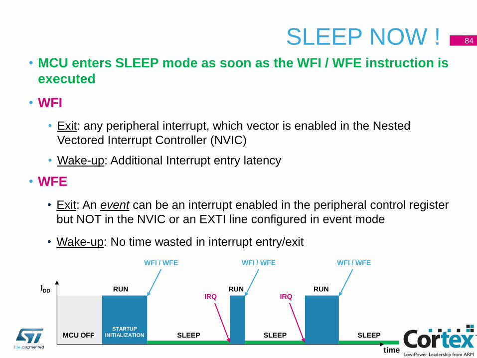
• MCU enters SLEEP mode as soon as the WFI / WFE instruction is
executed
• WFI
• Exit: any peripheral interrupt, which vector is enabled in the Nested
Vectored Interrupt Controller (NVIC)
• Wake-up: Additional Interrupt entry latency
• WFE
• Exit: An event can be an interrupt enabled in the peripheral control register
but NOT in the NVIC or an EXTI line configured in event mode
• Wake-up: No time wasted in interrupt entry/exit
SLEEP NOW ! 84
MCU OFF SLEEP SLEEP SLEEP
RUN RUN RUN
STARTUP
INITIALIZATION
IRQ IRQ
WFI / WFE WFI / WFE
IDD
time
WFI / WFE

• MCU enters SLEEP or DEEP SLEEP mode as soon as it exits the
lowest priority interrupt service routine (ISR)
• Controlled by SLEEPONEXIT bit in Cortex-Mx System Control
Register of System Control Block (SCB_SCR)
• Exit: any peripheral interrupt acknowledged by the Nested Vectored
Interrupt Controller (NVIC)
• Wake-up: The processor state is not un-stacked → faster wake up on
interrupt
SLEEP ON EXIT ! 85
MCU OFF SLEEP SLEEP SLEEP
RUN RUN (ISRs) RUN (ISRs)
STARTUP
INITIALIZATION
IRQ IRQ
IDD
time
WFI
Low-Power Modes
STM32L0 implementation
86
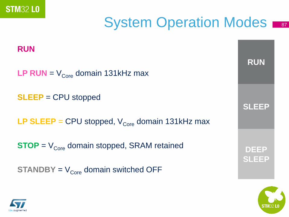
System Operation Modes
RUN
LP RUN = VCore domain 131kHz max
SLEEP = CPU stopped
LP SLEEP = CPU stopped, VCore domain 131kHz max
STOP = VCore domain stopped, SRAM retained
STANDBY = VCore domain switched OFF
87
DEEP
SLEEP
SLEEP
RUN
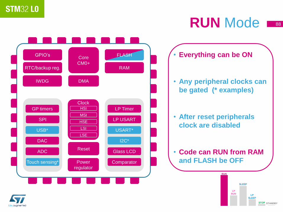
88 RUN Mode
LP
RUN
SLEEP
LP
SLEEP
STOP STANDBY
RUN
DMA
Core
CM0+
Power
regulator
LP Timer
FLASH
RAM
Clock
LP USART
USART*
GP timers
DAC
USB*
SPI
Glass LCD
Comparator Touch sensing*
ADC
I2C*
GPIO’s
RTC/backup reg.
IWDG
Reset
• Everything can be ON
• Any peripheral clocks can
be gated (* examples)
• After reset peripherals
clock are disabled
• Code can RUN from RAM
and FLASH be OFF
HSE
HSI
MSI
LSE
LSI

Clock controller: the “Gearbox”
CSS
HSE Osc
OSC_OUT
OSC_IN
1 -24
MHz
up to 32
MHz
SYSCLK x3...x48,
/2,/3,/4 PLL PLLCLK
HSI RC 16MHz
MSI RC
64KHz, …, 4.2 MHz
ADCCLK
SYSCLK
HSI
HSE
PLLCLK
MCO /1,/2,/4,/8,/
16
MSI
LSE
LSI
LSI RC
32.768KHz
/2, 4,
8,16
LSE OSc
OSC32_IN
OSC32_OUT
~37KHz IWDGCLK
RTCCLK
LCDCLK
Low speed path: for low
consumption while CPU is static
Medium speed path: for low
consumption while CPU is at low
frequency
High speed path: for performance
capable to scale to the desired level
frequency (PLL)- change on the fly of
frequency
90
CSS
HSI48 RC
CRS
USBCLK
RBGCLK
48MHz

Clock Sources Parameters 91
Clock
Source
Frequency Conso Precision
25°C/0-85°C
Wakeup
time
MSI ( default )
65kHz-4.2MHz ( 2.1MHz default )
0.7-15µA ±0.5% / ±3% 3.5 µs (4.2MHz, Vcore
Range 1/2)
HSI 16MHz 100µA ±1% / ±2.5% 3.7 µs
HSE external crystal
1-24MHz ~500µA ~±0.01% ( 100ppm )
1ms
HSE external clock
1-32MHz N/A N/A
PLL 2-32MHz ~350µA N/A 100µs ( 2MHz input )
LSI 37kHz 0.4µA 50% 200µs (max)
LSE external crystal
32.768kHz ( typically )
~0.3µA ~0.002% ( 20ppm )
~1s
LSE external clock
1-1000kHz N/A N/A
+ Clock Source
Wake-Up time
LSE usually started only once after power-on
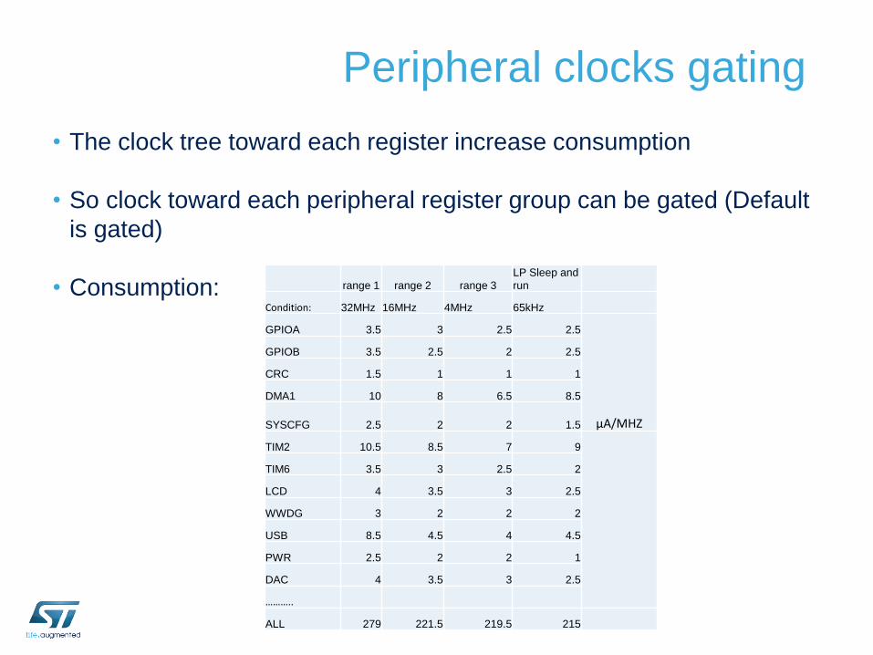
Peripheral clocks gating
• The clock tree toward each register increase consumption
• So clock toward each peripheral register group can be gated (Default
is gated)
• Consumption: range 1 range 2 range 3 LP Sleep and
run
Condition: 32MHz 16MHz 4MHz 65kHz
GPIOA 3.5 3 2.5 2.5
µA/MHZ
GPIOB 3.5 2.5 2 2.5
CRC 1.5 1 1 1
DMA1 10 8 6.5 8.5
SYSCFG 2.5 2 2 1.5
TIM2 10.5 8.5 7 9
TIM6 3.5 3 2.5 2
LCD 4 3.5 3 2.5
WWDG 3 2 2 2
USB 8.5 4.5 4 4.5
PWR 2.5 2 2 1
DAC 4 3.5 3 2.5
………..
ALL 279 221.5 219.5 215
System blocks
Power Control (PWR)
95
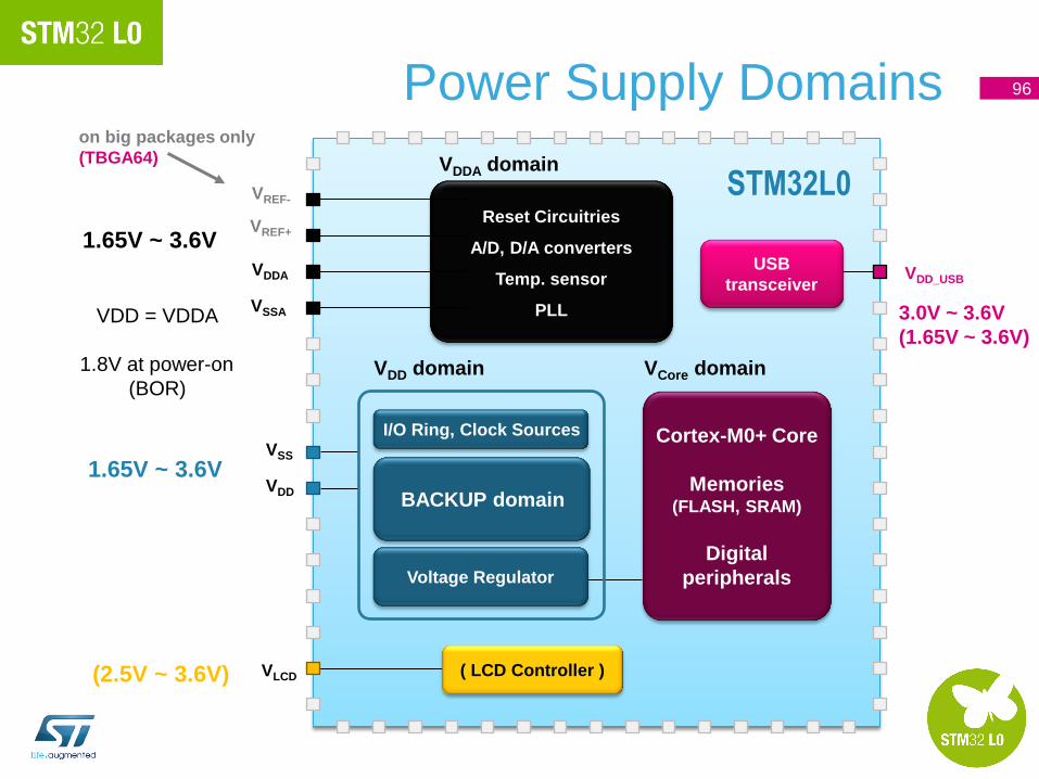
Power Supply Domains 96
1.65V ~ 3.6V
1.65V ~ 3.6V
on big packages only
(TBGA64)
VLCD
VREF-
VREF+ Reset Circuitries
A/D, D/A converters
Temp. sensor
PLL
VDDA domain
Cortex-M0+ Core
Memories (FLASH, SRAM)
Digital
peripherals
VCore domain VDD domain
BACKUP domain
( LCD Controller )
Voltage Regulator
I/O Ring, Clock Sources
STM32L0
VDD = VDDA
1.8V at power-on
(BOR)
USB
transceiver
VSS
VDD
VDDA
VSSA
VDD_USB
3.0V ~ 3.6V
(1.65V ~ 3.6V)
(2.5V ~ 3.6V)

Voltage Regulator 97
• The Voltage regulator has three different modes
• Main voltage regulator mode (MVR)
– no output current limitation
– consumption of the regulator is ~8µA (typ)
• Ultra low power regulator mode
– output current limited
– consumption of the regulator is ~0.1µA (typ)
• Regulator OFF mode
– no output current
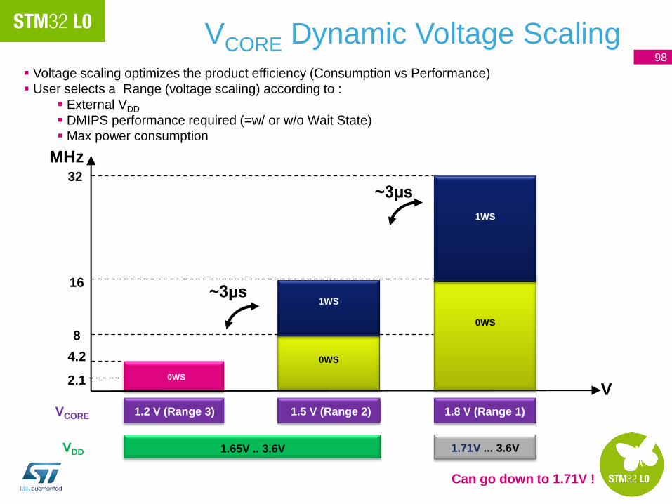
VCORE Dynamic Voltage Scaling
98
Voltage scaling optimizes the product efficiency (Consumption vs Performance)
User selects a Range (voltage scaling) according to :
External VDD
DMIPS performance required (=w/ or w/o Wait State)
Max power consumption
4.2
V
MHz
8
16
32
0WS
0WS
1WS
0WS
1WS
VDD 1.71V ... 3.6V 1.65V .. 3.6V
2.1
VCORE 1.2 V (Range 3) 1.5 V (Range 2) 1.8 V (Range 1)
98
~3µs
~3µs
Can go down to 1.71V !
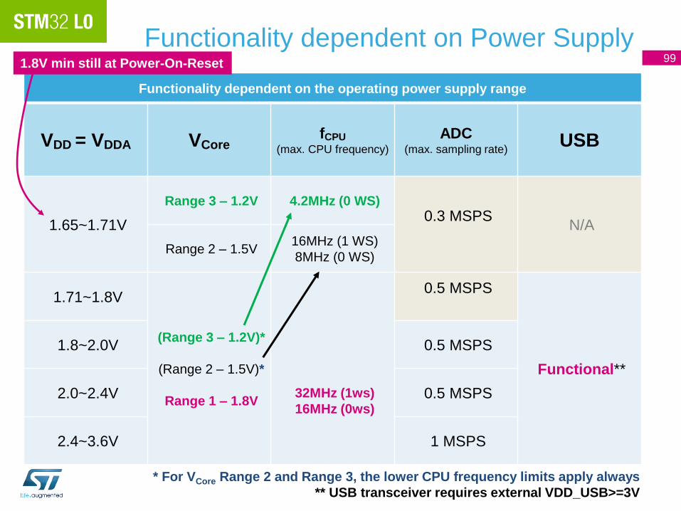
Functionality dependent on Power Supply
99
Functionality dependent on the operating power supply range
VDD = VDDA VCore fCPU
(max. CPU frequency)
ADC (max. sampling rate)
USB
1.65~1.71V
Range 3 – 1.2V 4.2MHz (0 WS)
0.3 MSPS
N/A
Range 2 – 1.5V 16MHz (1 WS)
8MHz (0 WS)
1.71~1.8V
(Range 3 – 1.2V)*
(Range 2 – 1.5V)*
Range 1 – 1.8V
32MHz (1ws)
16MHz (0ws)
0.5 MSPS
Functional**
1.8~2.0V 0.5 MSPS
2.0~2.4V 0.5 MSPS
2.4~3.6V 1 MSPS
99
* For VCore Range 2 and Range 3, the lower CPU frequency limits apply always
** USB transceiver requires external VDD_USB>=3V
1.8V min still at Power-On-Reset
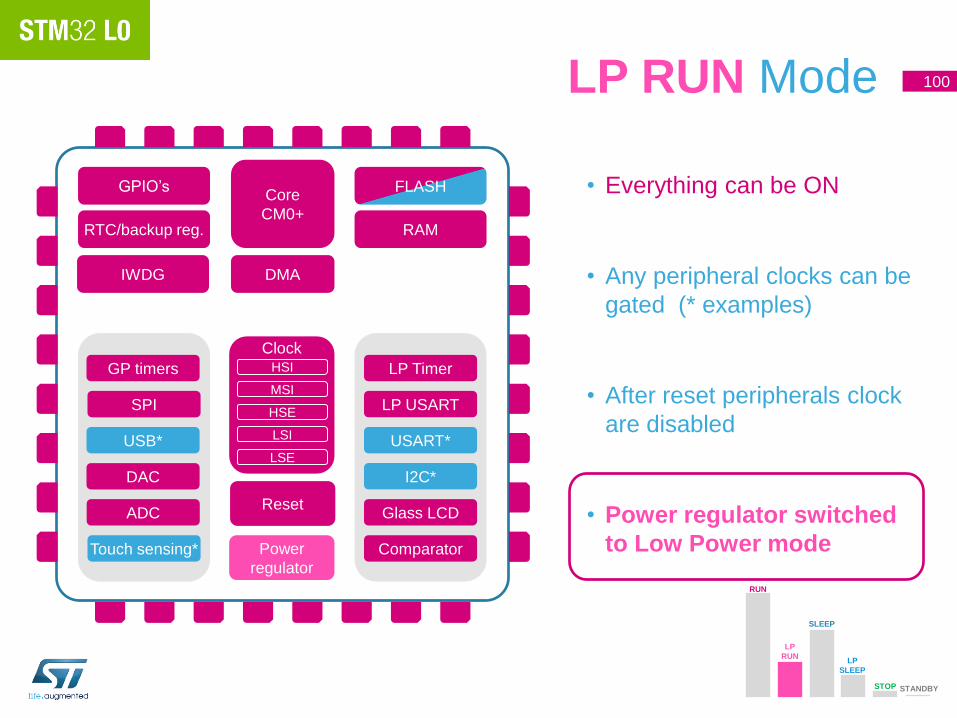
100 LP RUN Mode
• Everything can be ON
• Any peripheral clocks can be
gated (* examples)
• After reset peripherals clock
are disabled
• Power regulator switched
to Low Power mode
DMA
Core
CM0+
Power
regulator
LP Timer
FLASH
RAM
Clock
LP USART
USART*
GP timers
DAC
USB*
SPI
Glass LCD
Comparator Touch sensing*
ADC
I2C*
GPIO’s
RTC/backup reg.
IWDG
Reset
HSE
HSI
MSI
LSE
LSI
LP
RUN
SLEEP
LP
SLEEP
STOP STANDBY
RUN

101 SLEEP Mode
DMA
Core
CM0+
Power
regulator
LP Timer
RAM
Clock
LP USART
USART
GP timers
DAC
USB
SPI
Glass LCD
Comparator Touch sensing
ADC
I2C
GPIO’s
RTC/backup reg.
IWDG
Reset
• Core is stopped
• Peripherals are running
HSE
HSI
MSI
LSE
LSI
FLASH
LP
RUN
SLEEP
LP
SLEEP
STOP STANDBY
RUN
FLASH
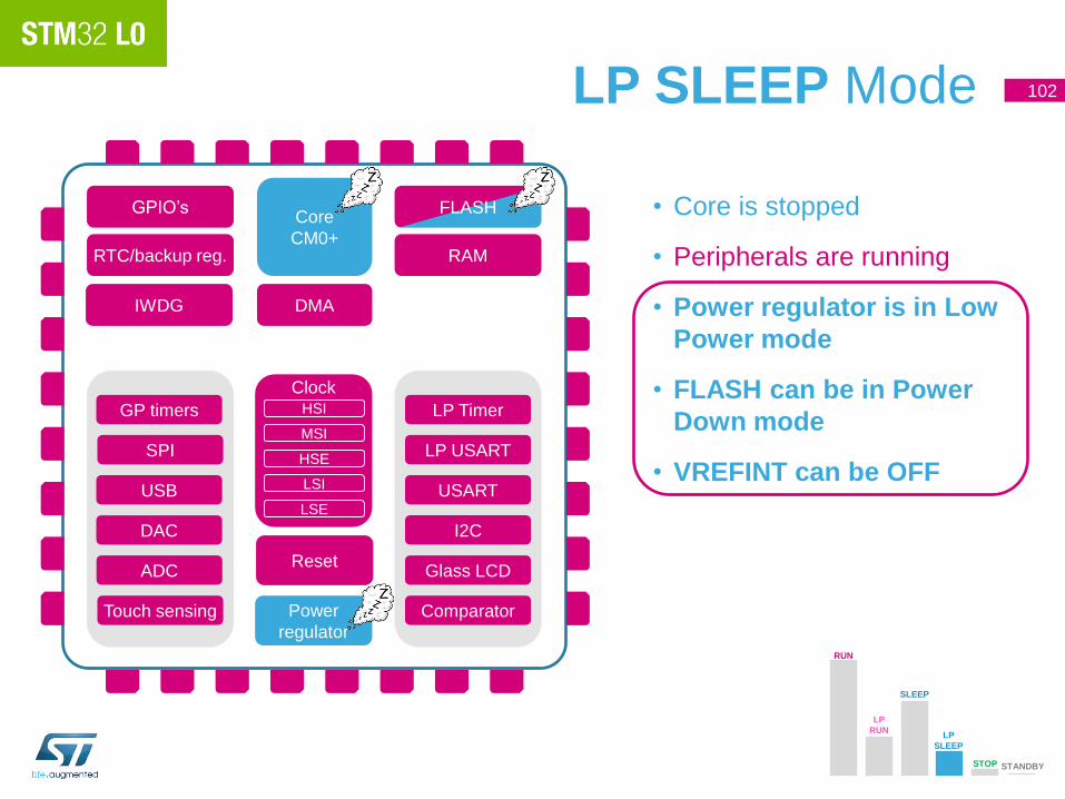
102 LP SLEEP Mode
• Core is stopped
• Peripherals are running
• Power regulator is in Low
Power mode
• FLASH can be in Power
Down mode
• VREFINT can be OFF
DMA
Core
CM0+
Power
regulator
LP Timer
RAM
Clock
LP USART
USART
GP timers
DAC
USB
SPI
Glass LCD
Comparator Touch sensing
ADC
I2C
GPIO’s
RTC/backup reg.
IWDG
Reset
HSE
HSI
MSI
LSE
LSI
LP
RUN
SLEEP
LP
SLEEP
STOP STANDBY
RUN
FLASH
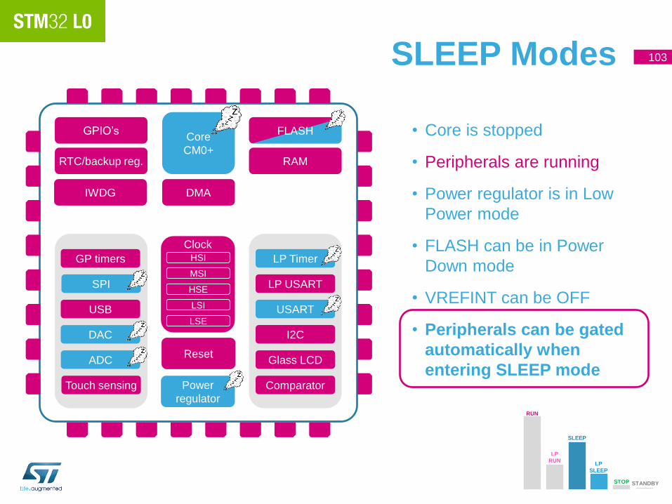
103 SLEEP Modes
• Core is stopped
• Peripherals are running
• Power regulator is in Low
Power mode
• FLASH can be in Power
Down mode
• VREFINT can be OFF
• Peripherals can be gated
automatically when
entering SLEEP mode
DMA
Core
CM0+
Power
regulator
LP Timer
RAM
Clock
LP USART
USART
GP timers
DAC
USB
SPI
Glass LCD
Comparator Touch sensing
ADC
I2C
GPIO’s
RTC/backup reg.
IWDG
Reset
HSE
HSI
MSI
LSE
LSI
LP
RUN
SLEEP
LP
SLEEP
STOP STANDBY
RUN
104 SLEEP Modes
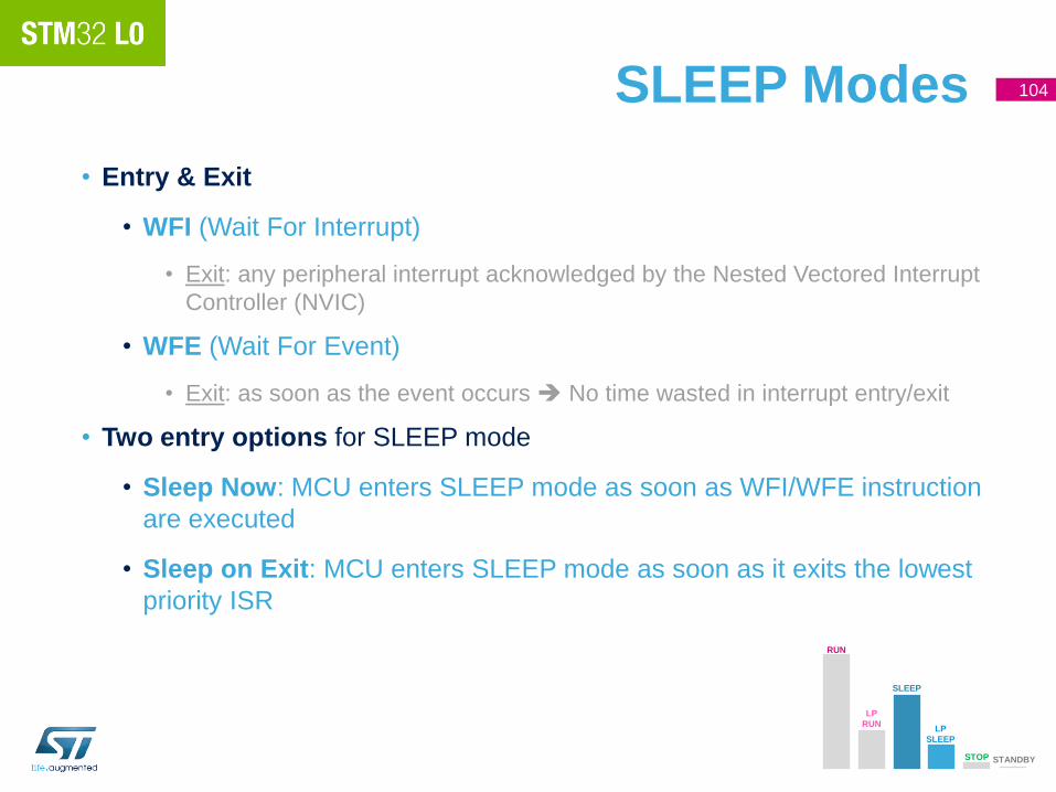
• Entry & Exit
• WFI (Wait For Interrupt)
• Exit: any peripheral interrupt acknowledged by the Nested Vectored Interrupt
Controller (NVIC)
• WFE (Wait For Event)
• Exit: as soon as the event occurs No time wasted in interrupt entry/exit
• Two entry options for SLEEP mode
• Sleep Now: MCU enters SLEEP mode as soon as WFI/WFE instruction
are executed
• Sleep on Exit: MCU enters SLEEP mode as soon as it exits the lowest
priority ISR
LP
RUN
SLEEP
LP
SLEEP
STOP STANDBY
RUN

Clock
105 STOP Mode
DMA
Core
CM0+
Power
regulator
LP Timer
FLASH
RAM
LP USART
USART
GP timers
DAC
USB
SPI
Glass LCD ADC
Touch sensing Comparator
I2C
GPIO’s
RTC/backup reg.
IWDG
Reset
HSE
HSI
MSI
LSE
LSI
• Core is stopped
• HSE, MSI clocks are OFF
• SRAM and registers
content is preserved
• Peripherals with HSI, LSI,
LSE clock option can be
ON
• GPIO’s keep their setup
LP
RUN
SLEEP
LP
SLEEP
STOP STANDBY
RUN
Clock
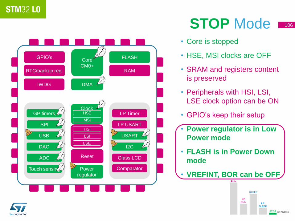
106 STOP Mode
DMA
Core
CM0+
Power
regulator
LP Timer
FLASH
RAM
LP USART
USART
GP timers
DAC
USB
SPI
Glass LCD ADC
Touch sensing Comparator
I2C
GPIO’s
RTC/backup reg.
IWDG
Reset
HSE
HSI
MSI
LSE
LSI
• Core is stopped
• HSE, MSI clocks are OFF
• SRAM and registers content
is preserved
• Peripherals with HSI, LSI,
LSE clock option can be ON
• GPIO’s keep their setup
• Power regulator is in Low
Power mode
• FLASH is in Power Down
mode
• VREFINT, BOR can be OFF
LP
RUN
SLEEP
LP
SLEEP
STOP STANDBY
RUN
107 STOP Mode
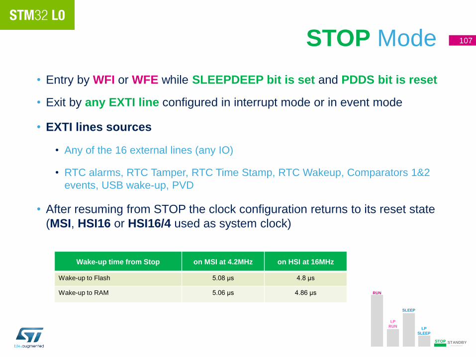
• Entry by WFI or WFE while SLEEPDEEP bit is set and PDDS bit is reset
• Exit by any EXTI line configured in interrupt mode or in event mode
• EXTI lines sources
• Any of the 16 external lines (any IO)
• RTC alarms, RTC Tamper, RTC Time Stamp, RTC Wakeup, Comparators 1&2
events, USB wake-up, PVD
• After resuming from STOP the clock configuration returns to its reset state
(MSI, HSI16 or HSI16/4 used as system clock)
Wake-up time from Stop on MSI at 4.2MHz on HSI at 16MHz
Wake-up to Flash 5.08 µs 4.8 µs
Wake-up to RAM 5.06 µs 4.86 µs
LP
RUN
SLEEP
LP
SLEEP
STOP STANDBY
RUN
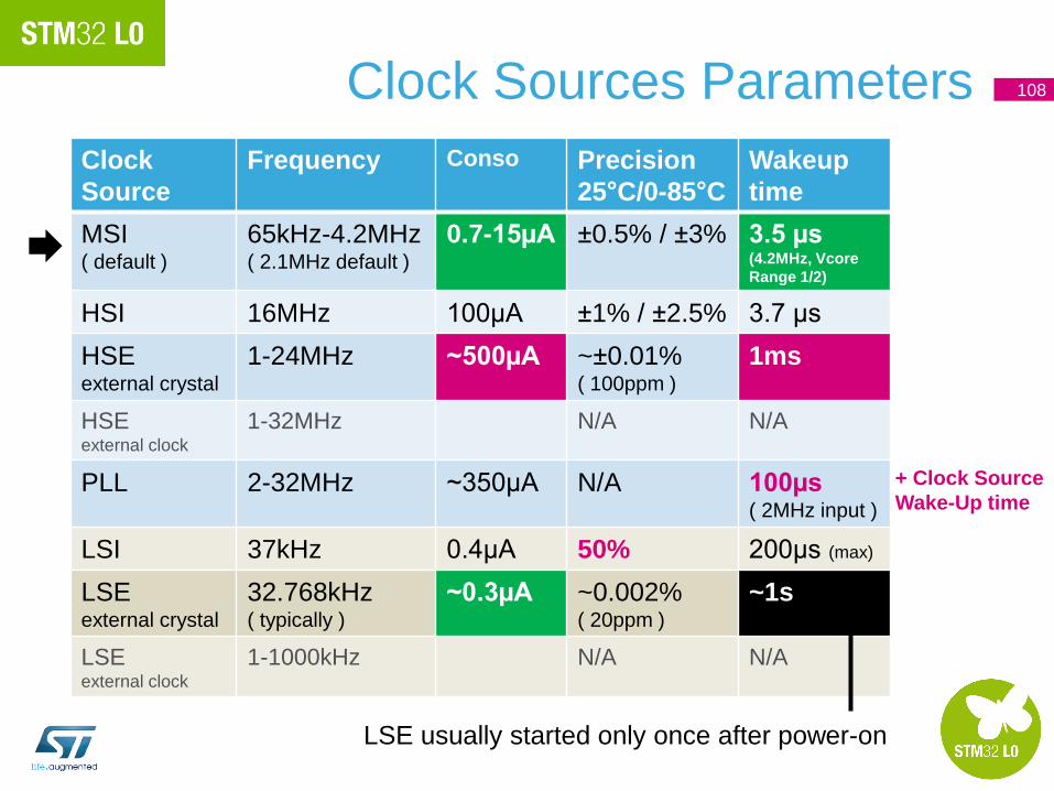
Clock Sources Parameters 108
Clock
Source
Frequency Conso Precision
25°C/0-85°C
Wakeup
time
MSI ( default )
65kHz-4.2MHz ( 2.1MHz default )
0.7-15µA ±0.5% / ±3% 3.5 µs (4.2MHz, Vcore
Range 1/2)
HSI 16MHz 100µA ±1% / ±2.5% 3.7 µs
HSE external crystal
1-24MHz ~500µA ~±0.01% ( 100ppm )
1ms
HSE external clock
1-32MHz N/A N/A
PLL 2-32MHz ~350µA N/A 100µs ( 2MHz input )
LSI 37kHz 0.4µA 50% 200µs (max)
LSE external crystal
32.768kHz ( typically )
~0.3µA ~0.002% ( 20ppm )
~1s
LSE external clock
1-1000kHz N/A N/A
+ Clock Source
Wake-Up time
LSE usually started only once after power-on

Clock
110 STANDBY Mode
DMA
Core
CM0+
Power
regulator
LP Timer
FLASH
RAM
LP USART
USART
GP timers
DAC
USB
SPI
Glass LCD ADC
Touch sensing Comparator
I2C
GPIO’s
RTC/backup reg.
IWDG
Reset
HSE
HSI
MSI
LSE
LSI
• Core and all peripherals
are OFF, except RTC and
IWDG if enabled
• HSE, MSI, HSI clocks are
OFF, LSI LSE can be ON
• SRAM and registers
content is lost, except
RTC, and standby circuitry
• GPIO’s are in high Z,
except Reset, RTC OUT
and WKUP 1,2,3
Reset RTC OUT WKUP 1,2,3 LP
RUN
SLEEP
LP
SLEEP
STOP STANDBY
RUN
111 STANDBY Mode
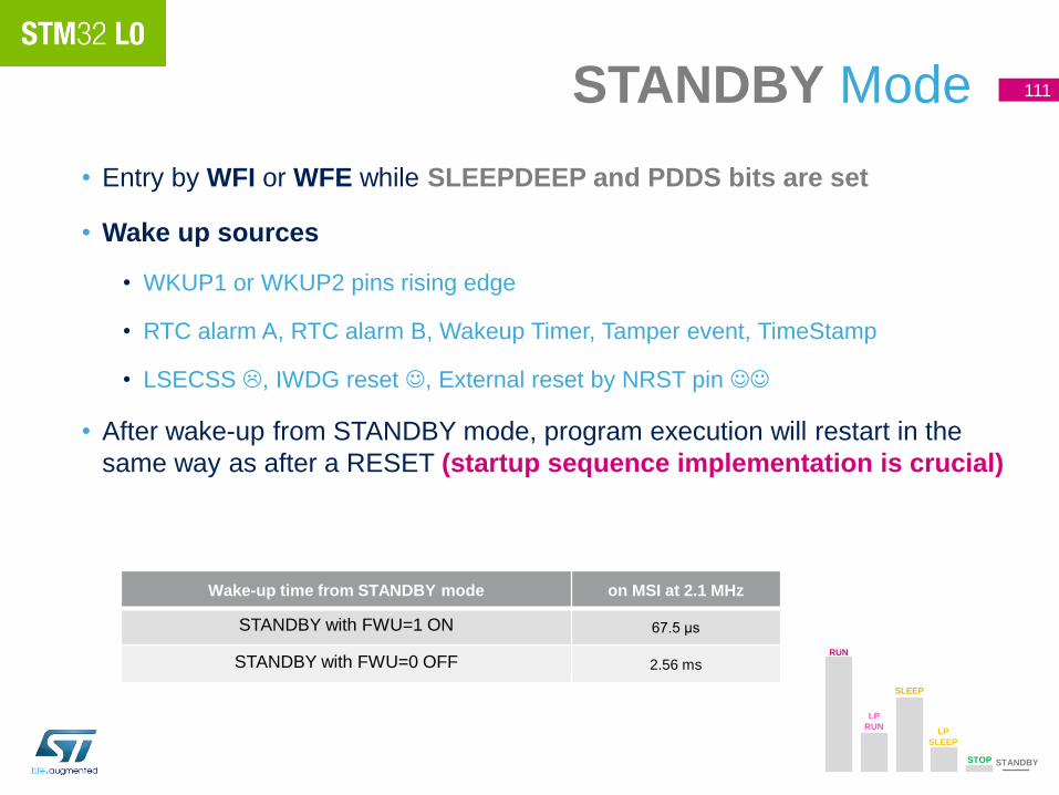
• Entry by WFI or WFE while SLEEPDEEP and PDDS bits are set
• Wake up sources
• WKUP1 or WKUP2 pins rising edge
• RTC alarm A, RTC alarm B, Wakeup Timer, Tamper event, TimeStamp
• LSECSS , IWDG reset , External reset by NRST pin
• After wake-up from STANDBY mode, program execution will restart in the
same way as after a RESET (startup sequence implementation is crucial)
Wake-up time from STANDBY mode on MSI at 2.1 MHz
STANDBY with FWU=1 ON 67.5 µs
STANDBY with FWU=0 OFF 2.56 ms
LP
RUN
SLEEP
LP
SLEEP
STOP STANDBY
RUN
RTC: +480nA
LSE: +100nA (low-drive, 32.768kHz crystal)
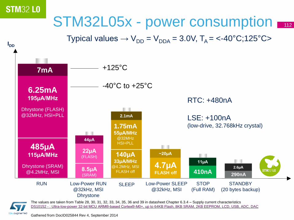
Neo 256K – Low Power consumption values STM32L05x - power consumption 112
Typical values → VDD = VDDA = 3.0V, TA = <-40°C;125°C>
IDD
6.25mA 195µA/MHz
Dhrystone (FLASH)
@32MHz, HSI+PLL
485µA 115µA/MHz
Dhrystone (SRAM)
@4.2MHz, MSI
7mA
RUN Low-Power RUN
@32kHz, MSI
Dhrystone
Low-Power SLEEP
@32kHz, MSI
STOP
(Full RAM)
STANDBY
(20 bytes backup)
The values are taken from Table 28, 30, 31, 32, 33, 34, 35, 36 and 39 in datasheet Chapter 6.3.4 – Supply current characteristics
DS10152 - : Ultra-low-power 32-bit MCU ARM®-based Cortex®-M0+, up to 64KB Flash, 8KB SRAM, 2KB EEPROM, LCD, USB, ADC, DAC
Gathered from DocID025844 Rev 4, September 2014
+125°C
-40°C to +25°C
410nA 290nA
2.6µA
44µA
22µA (FLASH)
8.5µA (SRAM)
4.7µA FLASH off
~20µA
1.75mA 55µA/MHz
@32MHz
HSI+PLL
140µA 33µA/MHz
@4.2MHz, MSI
FLASH off
2.1mA
SLEEP
11µA
References
• Datasheet
• 3.1 Low power modes
• 3.4.3 Voltage regulator
• 3.5 Clock management
• 6.3.4 Supply current characteristics
• Reference Manual
• 6 Power control (PWR)
• 7 Reset and clock control (RCC)
• Application note
• AN4445 STM32L05x ultra-low-power features overview
113
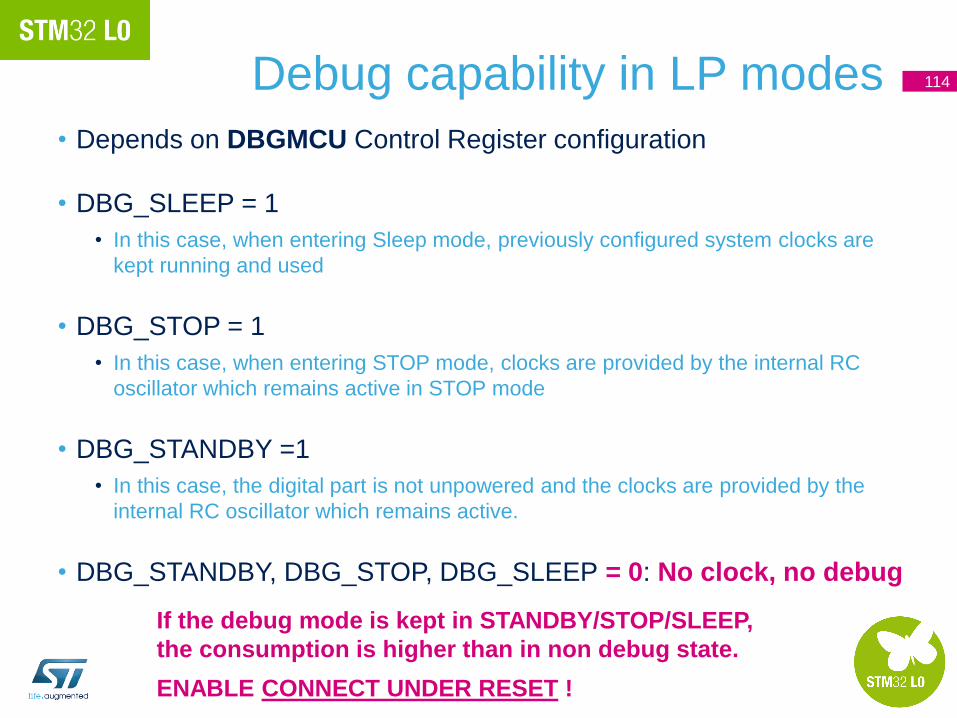
Debug capability in LP modes
• Depends on DBGMCU Control Register configuration
• DBG_SLEEP = 1
• In this case, when entering Sleep mode, previously configured system clocks are
kept running and used
• DBG_STOP = 1
• In this case, when entering STOP mode, clocks are provided by the internal RC
oscillator which remains active in STOP mode
• DBG_STANDBY =1
• In this case, the digital part is not unpowered and the clocks are provided by the
internal RC oscillator which remains active.
• DBG_STANDBY, DBG_STOP, DBG_SLEEP = 0: No clock, no debug
114
If the debug mode is kept in STANDBY/STOP/SLEEP,
the consumption is higher than in non debug state.
ENABLE CONNECT UNDER RESET !

Thank you
www.st.com/stm32l0