flash memory fault modeling and test algorithm development adviser: prof. cheng-wen wu 吳誠文...
Post on 20-Dec-2015
223 views
TRANSCRIPT
Flash Memory Fault Modeling and Test Algorithm Development
Flash Memory Fault Modeling and Test Algorithm Development
Adviser: Prof. Cheng-Wen Wu 吳誠文 教授Student: Jen-Chieh Yeh 葉人傑
May 06, 2004
LAB for Reliable ComputingDepartment of Electrical Engineering
National Tsing Hua UniversityHsinchu, Taiwan 30013
2/37
Outline Introduction
Flash Memory Overview
Flash Memory Testing Issues
Flash Disturb Fault Modeling
Flash Test Algorithm Development
Built-In Self-Test (BIST) Design
Experimental Results
Conclusions
3/37
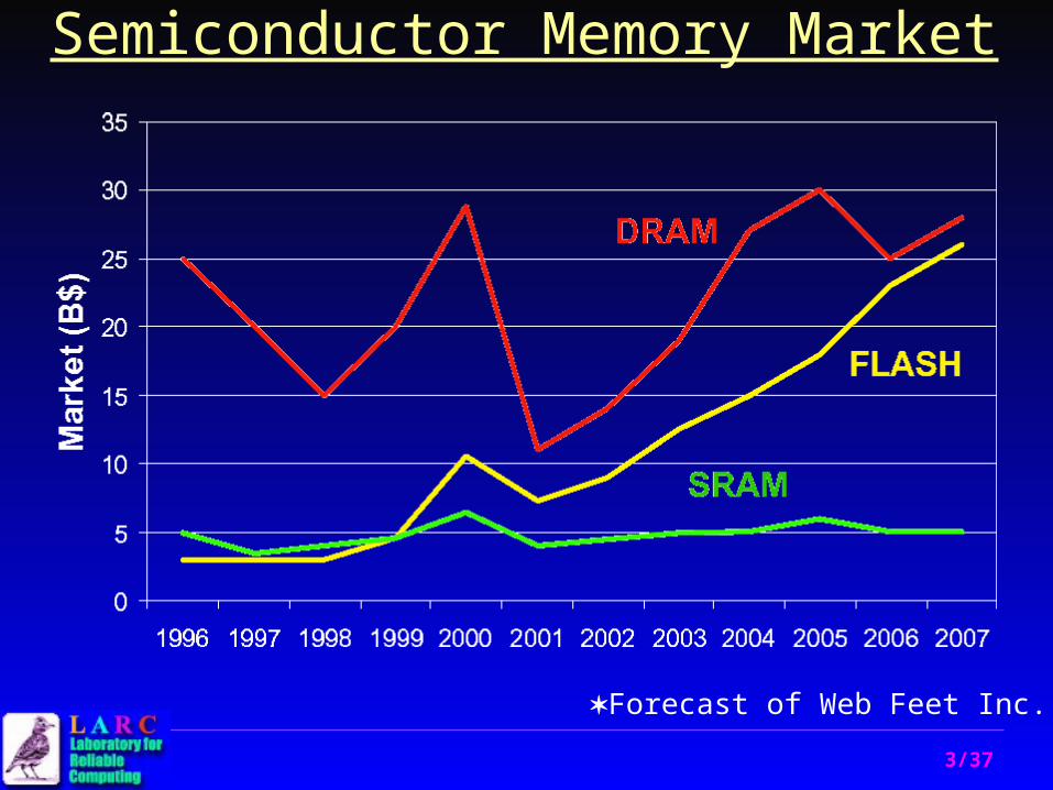
Semiconductor Memory Market
Forecast of Web Feet Inc.
4/37
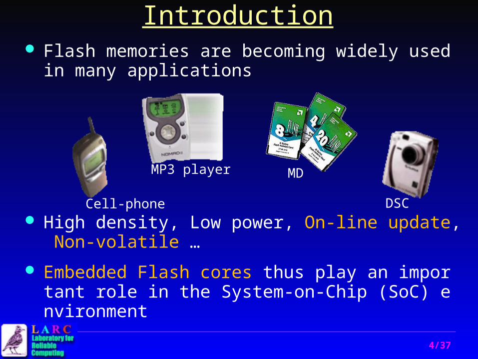
Introduction Flash memories are becoming widely used in m
any applications
High density, Low power, On-line update, Non-volatile …
Embedded Flash cores thus play an important role in the System-on-Chip (SoC) environment
Cell-phone
MP3 player MD
DSC

5/37
Flash Memory Applications
NAND
MCP
NOR
Se
rial A
cce
ssR
an
dom
Acc
ess
Low Density High Density
USB Drive
MP3
DSCPDA
G3 Phone
Cell Phone
PC BISO
Industrial Controls
DVD STB
SSD
Note: MCP = NOR or NAND based Flash devices including RAM in a Multi Chip Package
6/37
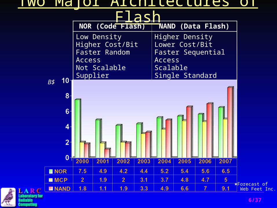
Two Major Architectures of FlashNOR (Code Flash) NAND (Data Flash)
Low DensityHigher Cost/BitFaster Random AccessNot ScalableSupplier Differences
Higher DensityLower Cost/BitFaster Sequential AccessScalableSingle Standard
B$
Forecast of Web Feet Inc.

7/37
NAND and NOR Architectures
NAND NOR
Bit-line
Word-line
Source line
8/37
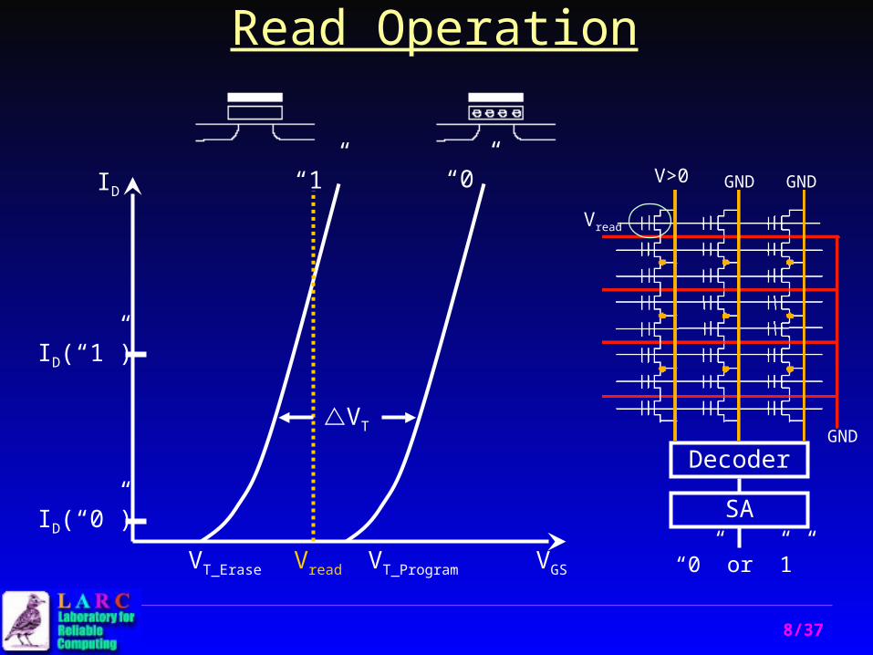
Read Operation
VT_Erase VT_Program VGSVread
ID(“0”)
ID(“1”)
ID “1” “0”
VT
Decoder
Vread
V>0 GND GND
GND
SA
“0” or ”1”

9/37
Write Mechanism
Program Operation (μs) Erase Operation (m s)
Vwl>>0
GND Vbl>0
Channel Hot Electron (CHE)injection in the floating gate at
the drain side
Vwl<<0
Vs>0 Vbl>0
Vbody>0
Fowler-Nordheim (FN) electron tunneling current throughthe tunnel oxide from the floating
gate to the silicon surface
Erasure is usually performed over a complete block or chip, and hence the name “Flash” Different process technologies and even manufactures may differ in their choice of the program/erase mechanism
10/37
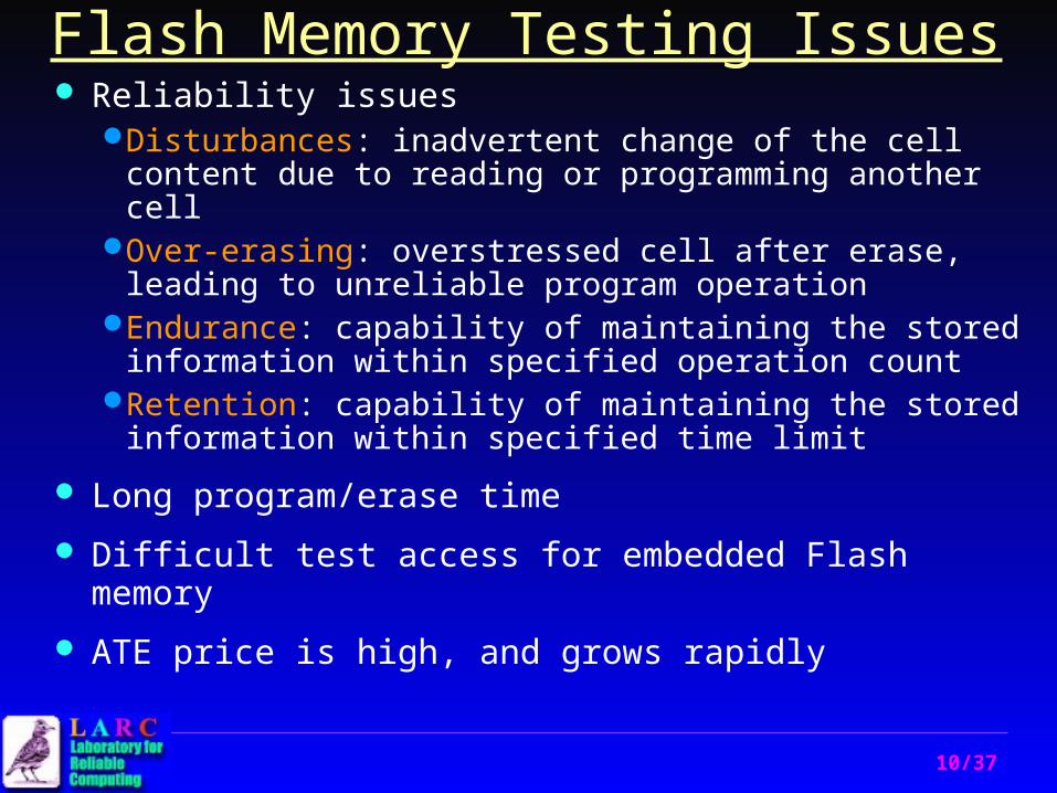
Flash Memory Testing Issues Reliability issues
Disturbances: inadvertent change of the cell content due to reading or programming another cell
Over-erasing: overstressed cell after erase, leading to unreliable program operation
Endurance: capability of maintaining the stored information within specified operation count
Retention: capability of maintaining the stored information within specified time limit
Long program/erase time
Difficult test access for embedded Flash memory
ATE price is high, and grows rapidly
11/37
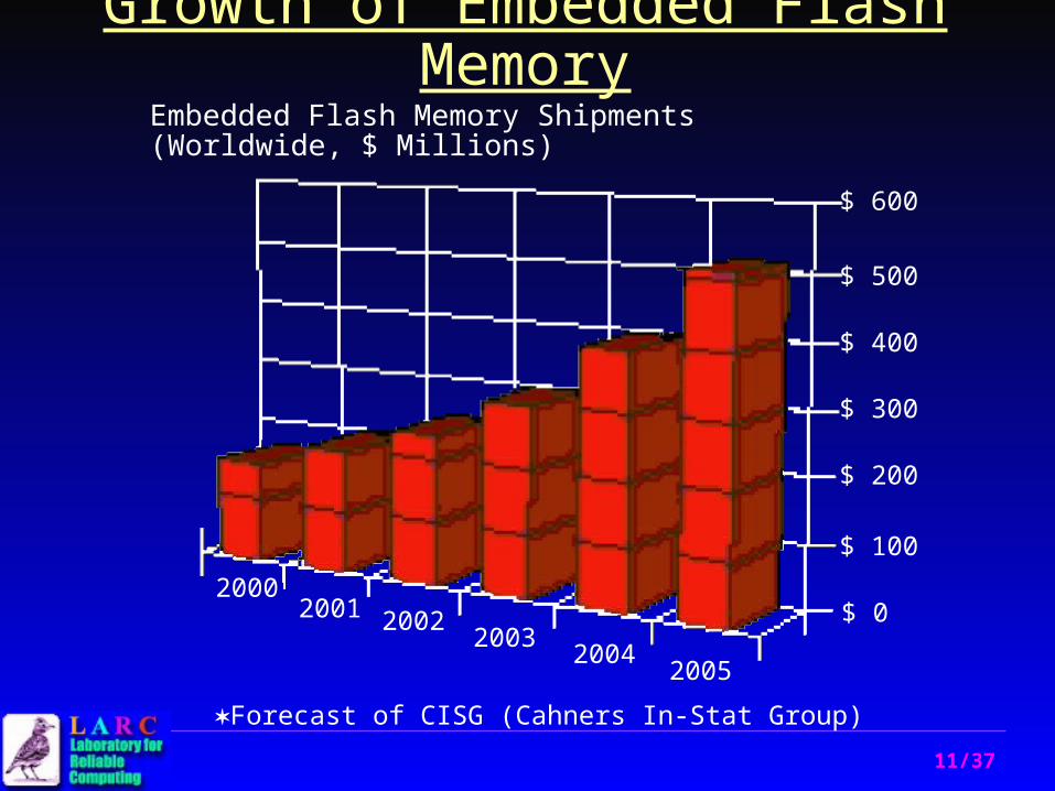
Growth of Embedded Flash MemoryEmbedded Flash Memory Shipments(Worldwide, $ Millions)
Forecast of CISG (Cahners In-Stat Group)
20002001 2002
20032004
2005
$ 0
$ 100
$ 200
$ 300
$ 400
$ 500
$ 600

12/37
Approaches Reasonable fault models for reliability-related
defects
Efficient test algorithms to reduce test time and increase fault coverage
Built-in self-test (BIST) circuit for embedded Flash memoriesReplace or reduce the requirement of ATE
“Built-in self-test and built-in self-repair will be essential to test embedded Flash memories and to maintain production throughput and yield.” [Quoted ITRS 2003]

13/37
Contribution to Flash Memory Testing
Study of Flash Memories
Flash Disturb Fault Modeling
Test Algorithm Development
Proposed First Built-In Self-Test Design for Flash
Complete Experimental Results
Fault Simulator:RAMSES-FT
Test Algorithm Generation by
Simulation: TAGS

14/37
Fault Modeling Fault model is defined faulty cell behavior
Fault model makes analysis possible
Fault model makes effectiveness testing
Fault model limits the scope of test pattern
Defects in
Layout
Defects in
Layout
Defects in
Transistor
Defects in
Transistor
Faulty Cell
Behavior
Faulty Cell
Behavior
Fault
Model
Fault
Model
15/37
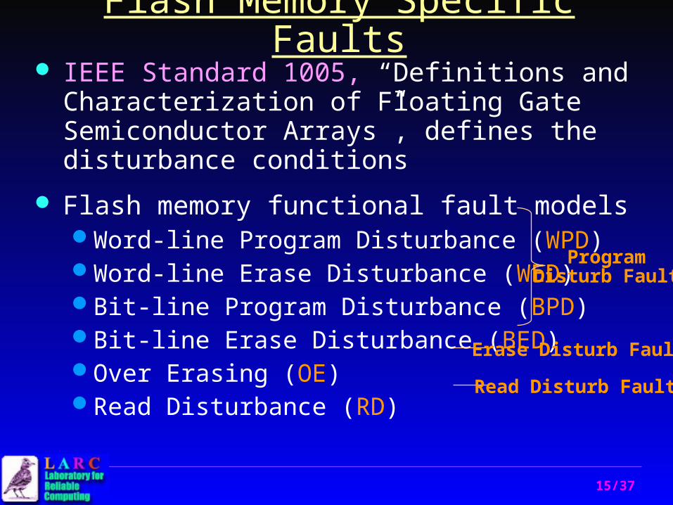
Flash Memory Specific Faults IEEE Standard 1005, “Definitions and
Characterization of Floating Gate Semiconductor Arrays”, defines the disturbance conditions
Flash memory functional fault modelsWord-line Program Disturbance (WPD)Word-line Erase Disturbance (WED)Bit-line Program Disturbance (BPD)Bit-line Erase Disturbance (BED)Over Erasing (OE)Read Disturbance (RD)
ProgramDisturb Fault
Erase Disturb Fault
Read Disturb Fault

16/37
Program Disturb Faults Word-line Program Disturbance (WPD)
A cell transits from 1 to 0 when another in the same word-line is being programmed (1 to 0)
Word-line Erase Disturbance (WED)A cell transits from 0 to 1 when another in the
same word-line is being programmed (1 to 0)
Bit-line Program Disturbance (BPD)A cell transits from 1 to 0 when another in the
same bit-line is being programmed (1 to 0)
Bit-line Erase Disturbance (BED)A cell transits from 0 to 1 when another in the
same bit-line is being programmed (1 to 0)

17/37
Word-line Program Disturbance WPD
V(H)
V(H)
V(L)
V(L)
V(Gd)
Conditions:
1.Victim cell initial value is a logic ‘1’
2.Aggressor “10” (program)
Victim “10” (program)Control Gate
Floating Gate
Source Drain
Substrate
G
S D
B

18/37
Word-line Erase Disturbance WED
Conditions:
1.Victim cell initial value is a logic ‘0’
2.Aggressor “10” (program)
Victim “01” (erase)Control Gate
Floating Gate
Source Drain
Substrate
G
S D
B
V(H)
V(H)
V(L)
V(L)
V(Gd)

19/37
Bit-line Erase Disturbance BED
Conditions:
1.Victim cell initial value is a logic ‘0’
2.Aggressor “10” (program)
Victim “01” (erase)Control Gate
Floating Gate
Source Drain
Substrate
G
S D
B
V(H)
V(H)
V(L)
V(L)
V(Gd)

20/37
Bit-line Program Disturbance BPD
V(H)
V(H)
V(L)
V(Gd)
During programming, erased cells on unselected
rows on a bit-line that is being programmed may
have a fairly deep depletion region formed under
them
Electrons entering this depletion region can be
accelerated by the electric field and injected over
the oxide potential barrier to adjacent floating
gates
Conditions:
1.Victim cell initial value is a logic ‘1’
2.Aggressor “10” (program) Victim “10” (program)
21/37
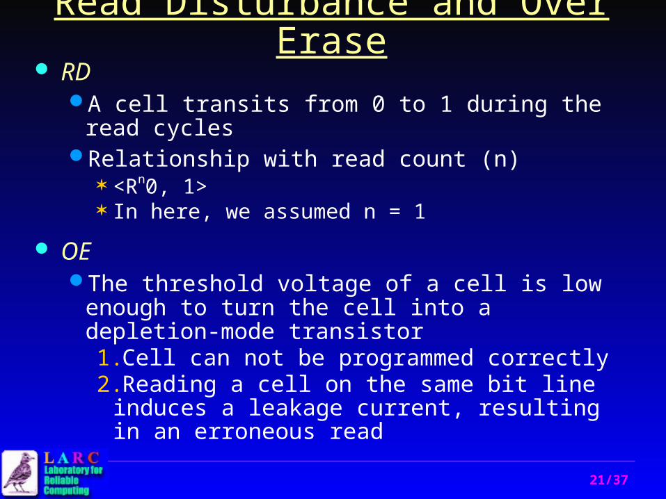
Read Disturbance and Over Erase RD
A cell transits from 0 to 1 during the read cyclesRelationship with read count (n)
<Rn0, 1> In here, we assumed n = 1
OEThe threshold voltage of a cell is low enough to
turn the cell into a depletion-mode transistor1.Cell can not be programmed correctly2.Reading a cell on the same bit line induces a
leakage current, resulting in an erroneous read
22/37
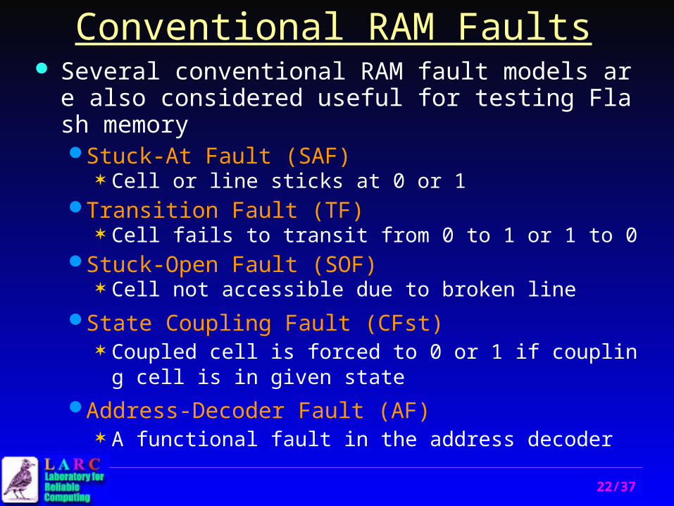
Conventional RAM Faults Several conventional RAM fault models are also
considered useful for testing Flash memoryStuck-At Fault (SAF)
Cell or line sticks at 0 or 1Transition Fault (TF)
Cell fails to transit from 0 to 1 or 1 to 0 Stuck-Open Fault (SOF)
Cell not accessible due to broken lineState Coupling Fault (CFst)
Coupled cell is forced to 0 or 1 if coupling cell is in given state
Address-Decoder Fault (AF) A functional fault in the address decoder
23/37
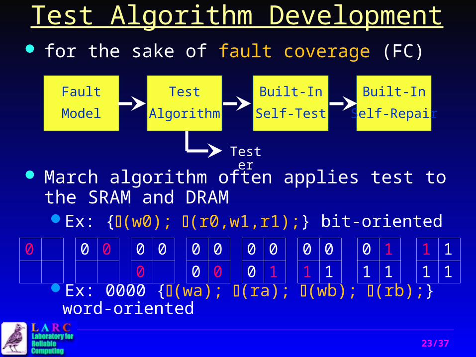
Test Algorithm Development for the sake of fault coverage (FC)
March algorithm often applies test to the SRAM and DRAMEx: {(w0); (r0,w1,r1);} bit-oriented
Ex: 0000 {(wa); (ra); (wb); (rb);} word-oriented
Fault
Model
Test
Algorithm
Built-In
Self-Test
Built-In
Self-Repair
Tester
0 0 0 0 0
0
0 0
0 0
0 0
0 1
0 0
1 1
0 1
1 1
1 1
1 1

24/37
Bit-oriented Flash Memory Test Conventional March tests can not detect all Flash
specific faults
No (w1) operation in Flash technology
Proposed March Flash Test (March-FT) {(f ); (r1,p0,r0); (r0); (f ); (r1,p0,r0); (r0);}Regular, easier to generate, covering more functional
faults and do not rely on the array geometry or layout topology
Notation Operations
f Erase
p0 Program
r1 or r0 Read 1 or 0
Notation Address Sequence
Ascending
Descending
Ascending or Descending

25/37
Word-oriented Flash Memory Test Word-oriented memory may have intra-word faults Add simple test with multiple standard backgrounds to
cover intra-word faults {(f ); (pa,ra); (f ); (pb,rb);}
Number of backgrounds is log2(m)+1m : word width1 : solid background
Example (m = 4):
0000 (f ); (rb,pa,ra); (ra); (f ); (rb,pa,ra); (ra);
0011 (f ); (pa,ra); (f ); (pb,rb); 0101 (f ); (pa,ra); (f ); (pb,rb);“0000” is solid background “0011” & “0101” are standard backgrounds
26/37
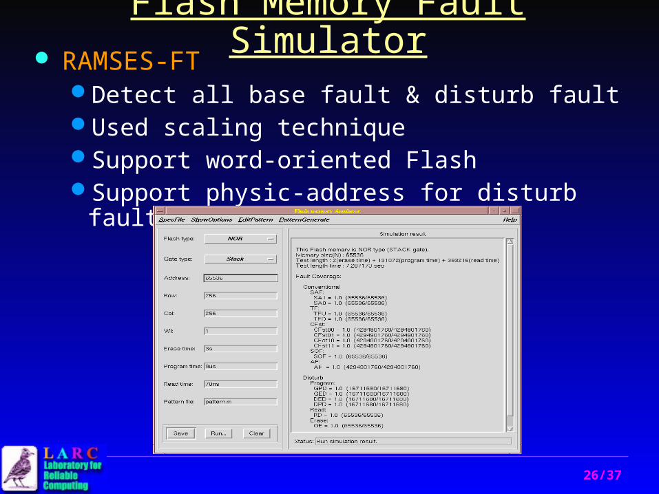
Flash Memory Fault Simulator RAMSES-FT
Detect all base fault & disturb faultUsed scaling techniqueSupport word-oriented FlashSupport physic-address for disturb fault

27/37
March-FT Simulation Result {(f); (r1,p0,r0); (r0); (f); (r1,p0,r0);
(r0)}This Flash memory is NOR type (STACK gate)
Memory size(N) : 65536
Test length : 2(chip erase time) + 131072(word program time) + 393216(word read time)
Test length time : 7.207173 sec
SAF : 100% (131072 / 131072) P.S.
TF : 100% (131072 / 131072) Flash Type = NOR
SOF : 100% (65536 / 65536) Gate Type = Stack
AF : 100% (4294901760 / 4294901760) Row Number = 256
CFst : 100% (17179607040 / 17179607040) Col Number = 256
WPD : 100% (16711680 / 16711680) Word Length = 1
WED : 100% (16711680 / 16711680) Chip erase time = 3 sec
BPD : 100% (16711680 / 16711680) Word program time = 9u sec
BED : 100% (16711680 / 16711680) Word read time = 70n sec
RD : 100% (65536 / 65536)
OE : 100% (65536 / 65536)
28/37
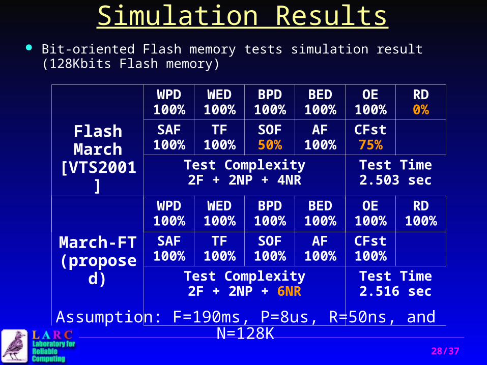
Flash March
[VTS2001]
WPD100%
WED100%
BPD100%
BED100%
OE100%
RD0%
SAF100%
TF100%
SOF50%
AF100%
CFst75%
Test Complexity2F + 2NP + 4NR
Test Time2.503 sec
Simulation Results Bit-oriented Flash memory tests simulation result
(128Kbits Flash memory)
March-FT(proposed
)
WPD100%
WED100%
BPD100%
BED100%
OE100%
RD100%
SAF100%
TF100%
SOF100%
AF100%
CFst100%
Test Complexity2F + 2NP + 6NR
Test Time2.516 sec
Assumption: F=190ms, P=8us, R=50ns, and N=128K
29/37
Simulation Results (cont.) Word-oriented Flash memory tests simulation result
(128Kx4bits Flash memory, word width: 4)
Assumption: F=190ms, P=8us, R=50ns, and N=128K
March FT(With
standard backgrounds
)
WPD100%
WED100%
BPD100%
BED100%
OE100%
RD100%
SAF100%
TF100%
SOF100%
AF intra100%
AF inter100%
CFst intra
100%
CFst inter
100%Test Complexity6F + 6NP + 10NR
Test Time7.497 sec
March FT (Onlysolid
background)
WPD100%
WED100%
WPD100%
WED100%
OE100%
RD100%
SAF100%
TF100%
SOF100%
AF intra0%
AF inter100%
CFst intra
50%
CFst inter100%
Test Complexity2F + 2NP + 6NR
Test Time 2.516 sec
30/37
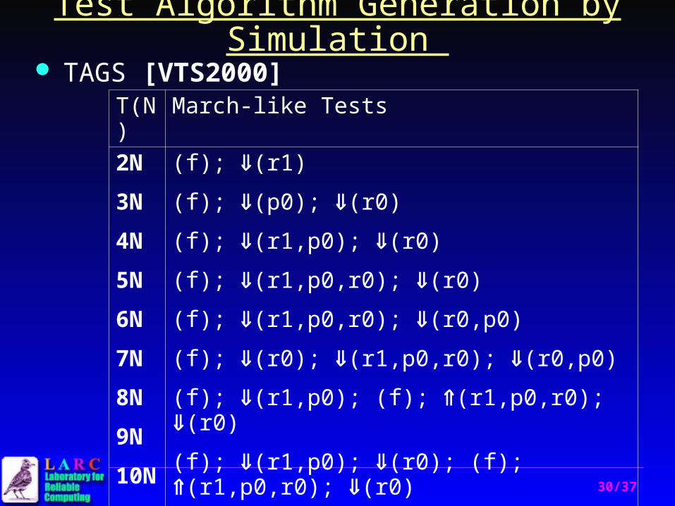
Test Algorithm Generation by Simulation TAGS [VTS2000]
T(N)
March-like Tests
2N
3N
4N
5N
6N
7N
8N
9N
10N
(f); (r1)
(f); (p0); (r0)
(f); (r1,p0); (r0)
(f); (r1,p0,r0); (r0)
(f); (r1,p0,r0); (r0,p0)
(f); (r0); (r1,p0,r0); (r0,p0)
(f); (r1,p0); (f); (r1,p0,r0); (r0)
(f); (r1,p0); (r0); (f); (r1,p0,r0); (r0)
(f); (r1,p0,r0); (r0); (f); (r1,p0,r0); (r0)
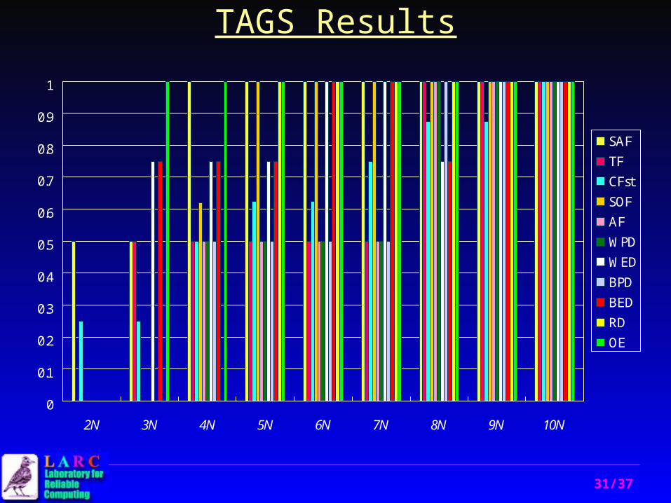
31/37
TAGS Results
0
0.1
0.2
0.3
0.4
0.5
0.6
0.7
0.8
0.9
1
2N 3N 4N 5N 6N 7N 8N 9N 10N
SAF
TF
CFst
SOF
AF
WPD
WED
BPD
BED
RD
OE

32/37
BIST Advantages Functional test (Go / No go) Tester functional easily (Few Logic I/O) Test throughput increased (Pin Count Reductio
n) Test program simply (Engineer Mode) System-on-Chip (SoC) testing easily
Flash
coreBIST
CLK
BNSGo/NoGo
BMS
Normal Mode Signal
MUX
33/37
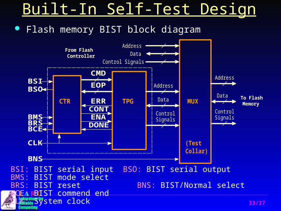
Built-In Self-Test Design Flash memory BIST block diagram
BSI: BIST serial input BSO: BIST serial output BMS: BIST mode selectBRS: BIST reset BNS: BIST/Normal select BCE: BIST commend endCLK: System clock
To FlashMemory
From FlashController
BMS
CLK
ERRCONT
DONEENA
EOP
Collar)(Test
CMD
TPG
BSOBSI
BRSBCE
MUX
BNS
CTR
DataAddress
Address
SignalsControl
DataData
SignalsControl
Address
Control Signals

34/37
Case I A typical 4Mbits (512K x 8) embedded Flash memory
core with BIST circuitry
Address Buffer
HV Generator
FlashCell Array
Y - Decoder &
Test Mode
Address
BIST
Control
BSIBSOBMSBRSBCECLKBNS
OEWE
CE
Address
Data
signalsControl
signalsControl
AddressData
DataTest Collar
Controlsignals
Test modesignals
Y - MUX
Sense Amp.I/O Buffer &
X - D
ecoder
Registers
Logic
35/37
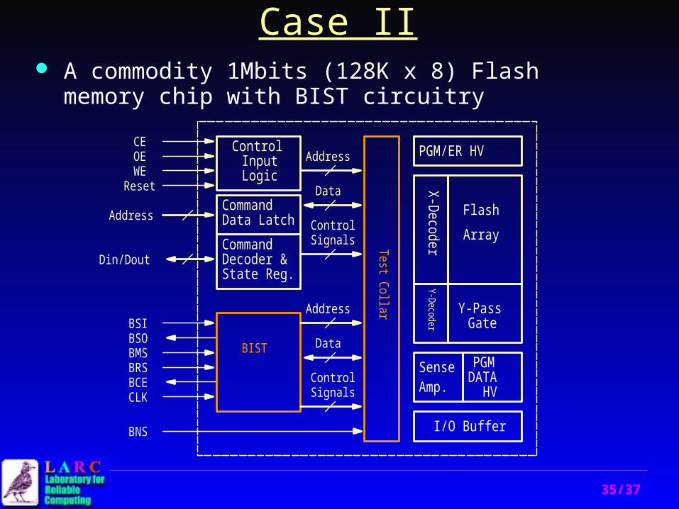
Case II A commodity 1Mbits (128K x 8) Flash memory chip with
BIST circuitry
CommandData LatchCommandDecoder &State Reg.
ArrayFlash
X-D
ecoderY-D
ecoder GateY-Pass
I/O Buffer
PGM/ER HV
SenseAmp.
PGM
HVDATA
Test Collar
ControlInputLogic
CEOEWE
Address
Din/Dout
ControlSignals
Address
Data
BNS
BISTBSO
BRSBCECLK
BMS
ControlSignals
Address
Data
Reset
BSI
36/37
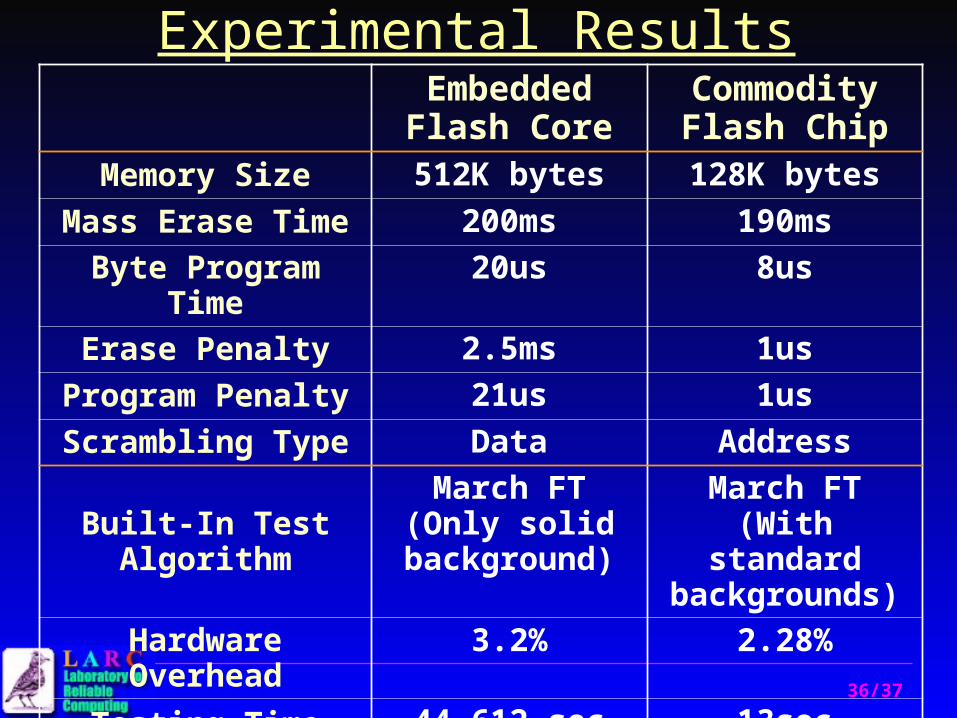
Experimental ResultsEmbedded Flash Core
Commodity Flash Chip
Memory Size 512K bytes 128K bytes
Mass Erase Time 200ms 190ms
Byte Program Time 20us 8us
Erase Penalty 2.5ms 1us
Program Penalty 21us 1us
Scrambling Type Data Address
Built-In Test Algorithm
March FT(Only solid
background)
March FT(With standard backgrounds)
Hardware Overhead 3.2% 2.28%
Testing Time 44.612 sec 13sec

37/37
Conclusions Bit-oriented and word-oriented Flash memory
tests are proposed
Implemented the BIST circuit for the embedded Flash memory core and commodity Flash memory chip
A Flash memory simulator has been developed to facilitate the analysis and generation of the tests
Developed March-like test methodology that can be used and reused for various Flash memories
Our future work is to support more Flash memory types and other realistic fault models, and to develop a diagnosis and repair methodology for Flash memories

Thank you for your attention!