fundamentals of optoelectronic materials and devices...
TRANSCRIPT

Fundamentals of Optoelectronic Materials and Devices
光電材料與元件基礎
Hsing-Yu Tuan (段興宇)
Department of Chemical Engineering, National Tsing-Hua University
Light Emitting Diodes: Principle
hυ - Eg
Eg (b)
V
(a)
p n+
Eg
eVo
EF
p n+
Electron in CBHole in VB
Ec
Ev
Ec
Ev
EF
eVo
Electron energy
Distance into device
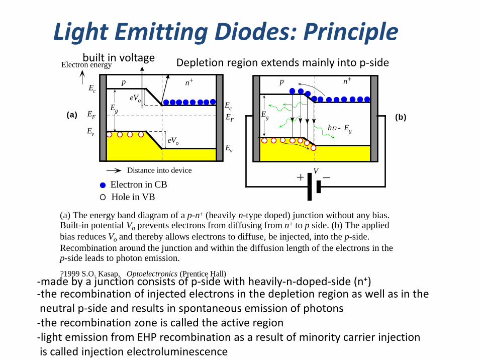
(a) The energy band diagram of a p-n+ (heavily n-type doped) junction without any bias.Built-in potential Vo prevents electrons from diffusing from n+ to p side. (b) The appliedbias reduces Vo and thereby allows electrons to diffuse, be injected, into the p-side.Recombination around the junction and within the diffusion length of the electrons in thep-side leads to photon emission.
?1999 S.O. Kasap, Optoelectronics (Prentice Hall)-made by a junction consists of p-side with heavily-n-doped-side (n+)
Depletion region extends mainly into p-side built in voltage
-the recombination of injected electrons in the depletion region as well as in the neutral p-side and results in spontaneous emission of photons -the recombination zone is called the active region -light emission from EHP recombination as a result of minority carrier injection is called injection electroluminescence

E1
hυ13E2
Metastablestate
E1
E3
E2
hυ32
E1
E3
E2
E1
E3
E2
hυ2hυ21
Coherent photons
OUT
(a) (b) (c) (d)
E3
The principle of the LASER. (a) Atoms in the ground state are pumped up to the energy level E3 byincoming photons of energy hυ13 = E3–E1. (b) Atoms at E3 rapidly decay to the metastable state atenergy level E2 by emitting photons or emitting lattice vibrations; hυ32 = E3–E2. (c) As the states at E2are long-lived, they quickly become populated and there is a population inversion between E2 and E1.(d) A random photon (from a spontaneous decay) of energy hυ21 = E2–E1 can initiate stimulatedemission. Photons from this stimulated emission can themselves further stimulate emissions leading to anavalanche of stimulated emissions and coherent photons being emitted.
?1999 S.O. Kasap, Optoelectronics (Prentice Hall)
IN
Laser : population inversion
Note: -in normal case, only two energy levels can not achieve population inversion -external excitation first excite electron from E1 to E3 -the emission from E2 to E1 is called lasing emission -LASER: Light Amplification by Stimulated Emission of Radiation - an example: Cr+3 ion in a crystal of alumina Al2O3 (saphire)
Make Stimulated emission rate larger
)(8)(
)(3
3
21
21 hvhvc
sponRstimR ρ
π=
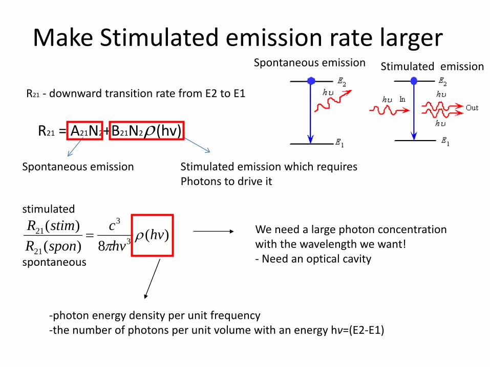
R21 - downward transition rate from E2 to E1
We need a large photon concentration with the wavelength we want! - Need an optical cavity
-photon energy density per unit frequency -the number of photons per unit volume with an energy hv=(E2-E1)
stimulated
spontaneous
R21 = A21N2+B21N2 (hv) ρ
Spontaneous emission Stimulated emission which requires Photons to drive it
Spontaneous emission Stimulated emission
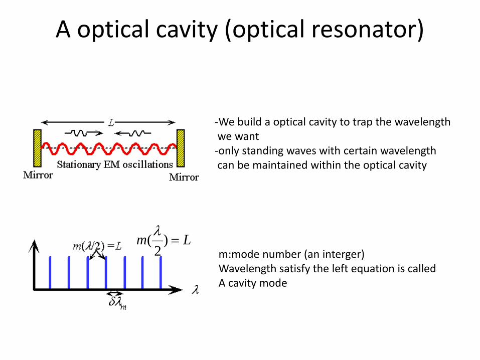
A optical cavity (optical resonator)
Lm =)2
(λ
-We build a optical cavity to trap the wavelength we want -only standing waves with certain wavelength can be maintained within the optical cavity
m:mode number (an interger) Wavelength satisfy the left equation is called A cavity mode

Laser diodes: utilization of PN junction
• Compared to other lasers (sapphire, CO2, HeNe, dye), semiconductor laser diodes are compact in size, electricity effective, efficient, long life, cheap, and versatile in color from UV to IR.
• Applications – CD,VCD,DVD players, CDROM, laser printer, laser pointer, bar code scanner, etc.

CB
g(E)
E
Impuritiesforming a band
(a) (b)
EFp
Ev
Ec
EFn
Ev
Ec
CB
VB
(a) Degenerate n-type semiconductor. Large number of donors form aband that overlaps the CB. (b) Degenerate p-type semiconductor.?1999 S.O. Kasap, Optoelectronics (Prentice Hall)
-the semiconductor that was excessively doped with donors or acceptors (1019-1020 cm-3) called degenerate semiconductor -such a semiconductor exhibits properties that are more metal-like -degenerate doping: the Fermi level EFP in the p-side is in the valence band(VB) and the EFn in the n-side is in the conduction band (CB) -a laser diode consists of “degenerately” doped p+ side with “degenerated” doped n+ side (p+n+ junction)
Degenerated semiconductor

p+ n+
EF n
(a)
Eg
Ev
Ec
Ev
Holes in V BElectrons in C B
Junction
Electrons Ec
p+
Eg
V
n+
(b)
EF n
eV
EF p
The energy band diagram of a degenerately doped p-n with no bias. (b) Banddiagram with a sufficiently large forward bias to cause population inversion andhence stimulated emission.
In v ers io nreg io n
EF p
EcEc
eVo
?1999 S.O. Kasap, Optoelectronics (Prentice Hall)
Structure: degenerately doped direct bandgap semiconductor pn junction
-laser diode structure: degenerately doped direct bandgap semiconductor pn junction -depletion region (active region) is very narrow -population inversion occurs when applying a voltage larger eV > Eg: the applied V diminishes the built-in potential to zero and electrons flow into the SCL -an incoming photon with energy Ec-Ev doesn’t excite an electron but stimulated by falling electrons
After applying large forward bias V
LED
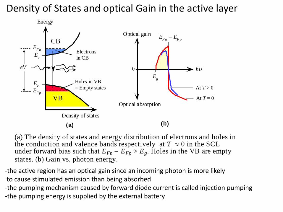
hυEg
Optical gain EF n − EF p
Optical absorption
0
Energy
Ec
Ev
CB
VB
(a) The density of states and energy distribution of electrons and holes inthe conduction and valence bands respectively at T ≈ 0 in the SCLunder forward bias such that EFn − EFp > Eg. Holes in the VB are emptystates. (b) Gain vs. photon energy.
Density of states
Electronsin CB
Holes in VB= Empty states
EF n
EF p
eV
At T > 0
At T = 0
(a) (b)
?1999 S.O. Kasap, Optoelectronics (Prentice Hall)
Density of States and optical Gain in the active layer
-the active region has an optical gain since an incoming photon is more likely to cause stimulated emission than being absorbed -the pumping mechanism caused by forward diode current is called injection pumping -the pumping energy is supplied by the external battery
L Electrode
Current
GaAs
GaAsn+
p+
Cleaved surface mirror
Electrode
Active region(stimulated emission region)
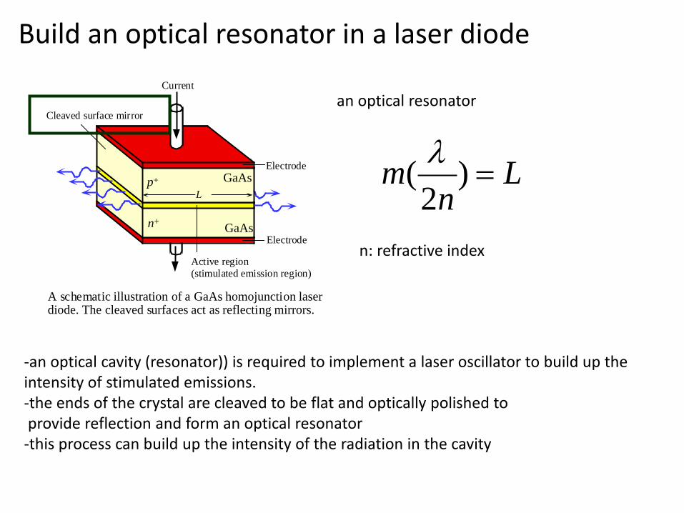
A schematic illustration of a GaAs homojunction laserdiode. The cleaved surfaces act as reflecting mirrors.
L
?1999 S.O. Kasap, Optoelectronics (Prentice Hall)
Build an optical resonator in a laser diode
-an optical cavity (resonator)) is required to implement a laser oscillator to build up the intensity of stimulated emissions. -the ends of the crystal are cleaved to be flat and optically polished to provide reflection and form an optical resonator -this process can build up the intensity of the radiation in the cavity
an optical resonator
Ln
m =)2
( λ
n: refractive index
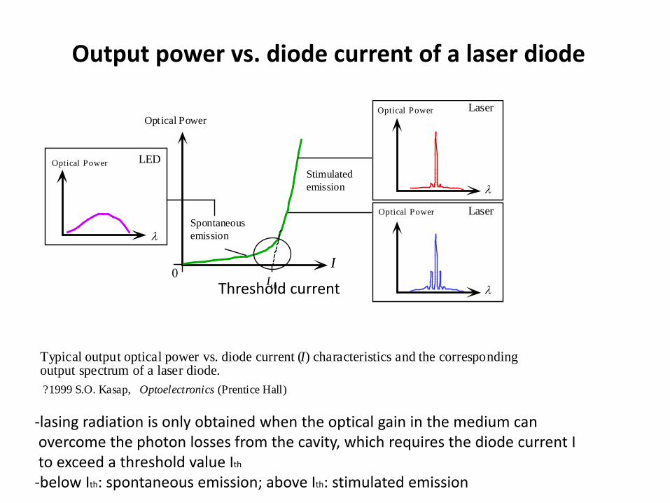
Output power vs. diode current of a laser diode
-lasing radiation is only obtained when the optical gain in the medium can overcome the photon losses from the cavity, which requires the diode current I to exceed a threshold value Ith
-below Ith: spontaneous emission; above Ith: stimulated emission
Typical output optical power vs. diode current (I) characteristics and the correspondingoutput spectrum of a laser diode.
λ
Laser
λ
LaserOptical Power
Optical Power
I0
λ
LEDOptical Power
Ith
Spontaneousemission
Stimulatedemission
Optical Power
?1999 S.O. Kasap, Optoelectronics (Prentice Hall)
Threshold current
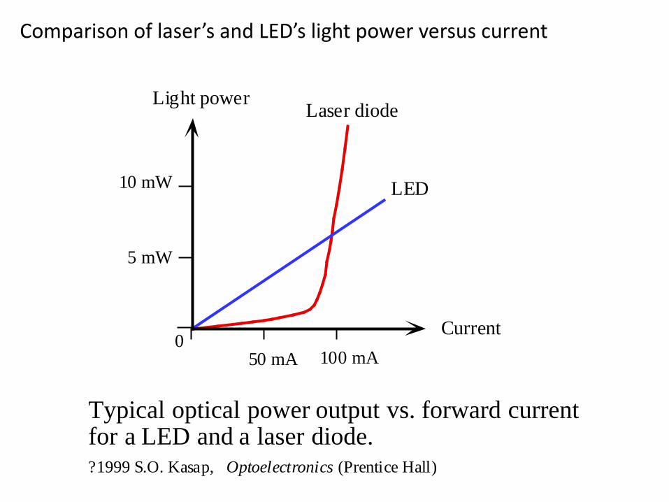
Typical optical power output vs. forward currentfor a LED and a laser diode.
Current0
Light power Laser diode
LED
100 mA50 mA
5 mW
10 mW
?1999 S.O. Kasap, Optoelectronics (Prentice Hall)
Comparison of laser’s and LED’s light power versus current

Heterostructure laser diode
Refractiveindex
Photondensity
Activeregion
∆n ~ 5%
2 eV
Holes in VB
Electrons in CB
AlGaAsAlGaAs
1.4 eV
Ec
Ev
Ec
Ev
(a)
(b)
pn p
∆Ec
(a) A doubleheterostructure diode hastwo junctions which arebetween two differentbandgap semiconductors(GaAs and AlGaAs).
2 eV
(b) Simplified energyband diagram under alarge forward bias.Lasing recombinationtakes place in the p-GaAs layer, theactive layer
(~0.1 µm)
(c) Higher bandgapmaterials have alower refractiveindex
(d) AlGaAs layersprovide lateral opticalconfinement.
(c)
(d)
?1999 S.O. Kasap, Optoelectronics (Prentice Hall)
GaAs
-a heterostructured laser diode can significantly reduce the threshold current (Ith) -we confine the injected electrons and holes to a narrow region, so that less current is needed to make population inversion -carriers are confined in the p-GaAs (active area) when the voltage is applied -gaAs layer is very thin, so the concentration of injected electrons can be increased quickly with moderate increases in forward current.
+ + +
Schematic illustration of the the structure of a double heterojunction stripecontact laser diode
Oxide insulator
Stripe electrode
SubstrateElectrode
Active region where J > Jth.(Emission region)
p-GaAs (Contacting layer)
n-GaAs (Substrate)
p-GaAs (Active layer)
Currentpaths
L
W
Cleaved reflecting surfaceEllipticallaserbeam
p-AlxGa1-xAs (Confining layer)
n-AlxGa1-xAs (Confining layer) 12 3
Cleaved reflecting surface
Substrate
?1999 S.O. Kasap, Optoelectronics (Prentice Hall)
Schematic illustration of a double heterojunction laser diode
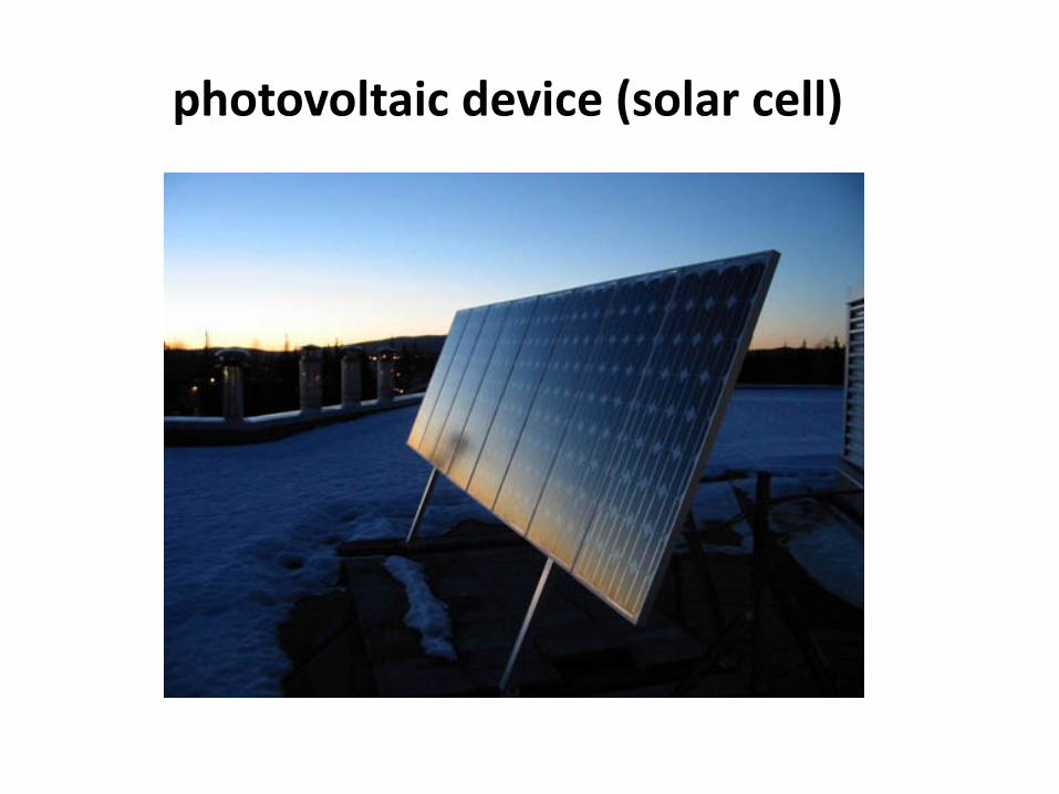
photovoltaic device (solar cell)
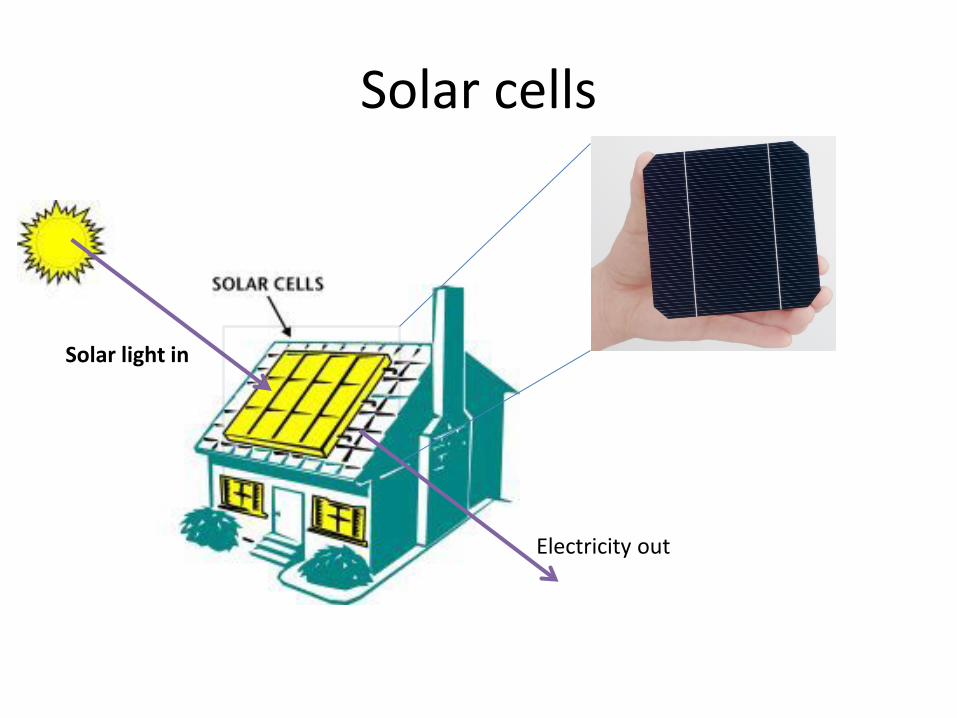
Solar cells
Solar light in
Electricity out
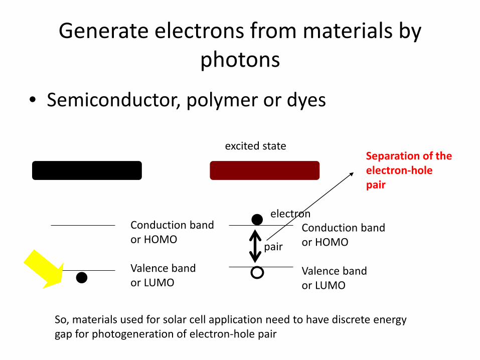
Generate electrons from materials by photons
• Semiconductor, polymer or dyes
Separation of the electron-hole pair
Conduction band or HOMO Valence band or LUMO
Conduction band or HOMO Valence band or LUMO
electron
pair
So, materials used for solar cell application need to have discrete energy gap for photogeneration of electron-hole pair
excited state

Silicon
CIGS
CdTe
GaAs
Inorganic Semiconductors

Elemental and Compound Semiconductors
5 B
6 C
7 N
8 O
13 Al
14 Si
15 P
16 S
29 Cu
30 Zn
31 Ga
32 Ge
33 As
34 Se
47 Ag
48 Cd
49 In
50 Sn
51 Sb
52 Te
I II III IV V VI
20

Definition of various radiation
AM0 :太陽光在大氣層外的平均照度稱為AM0,其功率約1300W/m^2 AM1 (90 °) :太陽光透過大氣層後與地表呈90度時的平均照度稱為AM1,其功率約925W/m^2 AM1.5 (45 °): AM1.5用來表示地面的平均照度,是指陽光透過大氣層後,與地表呈45°時 的光強度,功率約844W/m^2,在國際規範(IEC 891、IEC 904-1)將AM1.5 的功率定義為1000W/m^2。
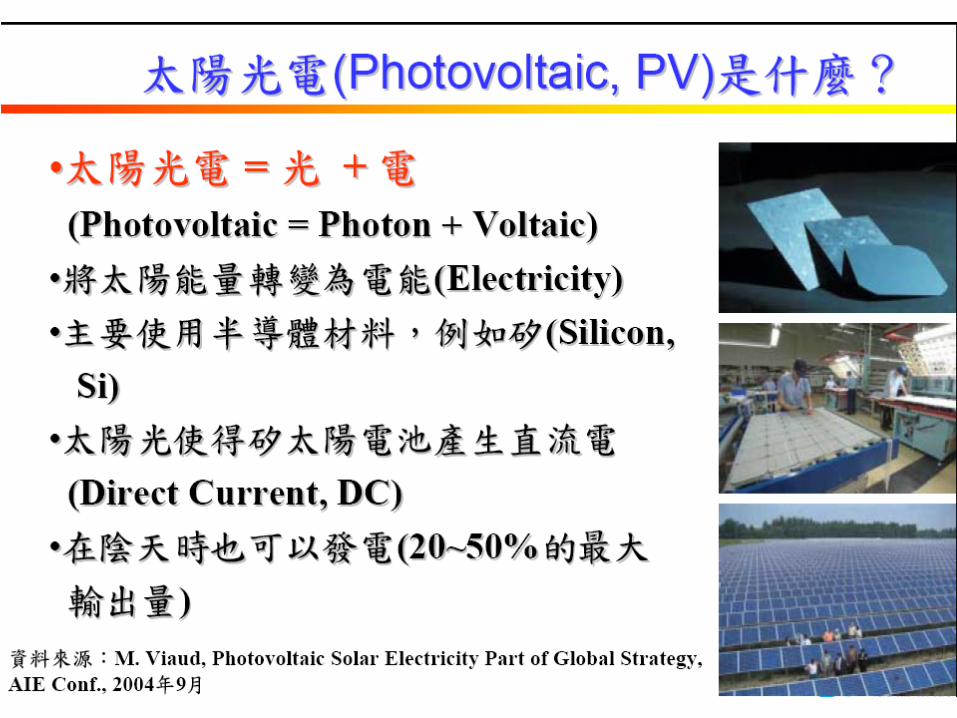
-photovoltaic = photon + voltaic
m=h/ho=secθ
Pick right materials
- Good absorption coefficient to harvest light - Suitable band gap

Absorption of semiconductors Phonon emission o r absorption
-We prefer direct semiconduct materials since they can absorb light more efficiently -Si and Ge’s absorption coefficient increase slowly with increased energy

∫
∫
<
<⋅
==
G
G
dShc
dSE
PIE
Eg
inc
incgg
λλ
λλ
λλλ
λλη
)(
)()(max
Theoretical maximum efficiency of a semiconductor
S(λ) =# of photons/area*time
-bandgap of semiconductor should not be wide get higher S(λ) -Electrons in the valence band can absorb energy of Eg, 2 Eg, 3Eg, but the excess energy can not be transformed to electric energy but transform to heat need higher Eg -very narrow band gap material can absorb most wavelength from sun, but transformed energy is small.
Pick suitable Eg (eV)
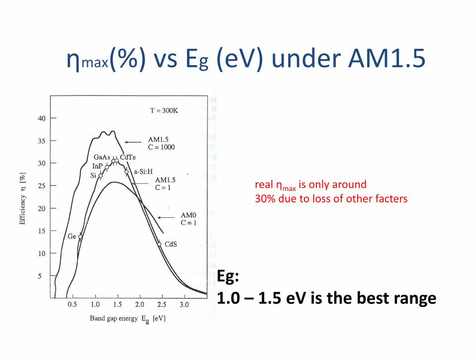
real ηmax is only around 30% due to loss of other facters
ηmax(%) vs Eg (eV) under AM1.5
Eg: 1.0 – 1.5 eV is the best range
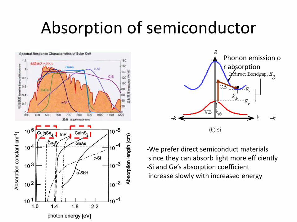
Absorption of semiconductor Phonon emission o r absorption
-We prefer direct semiconduct materials since they can absorb light more efficiently -Si and Ge’s absorption coefficient increase slowly with increased energy


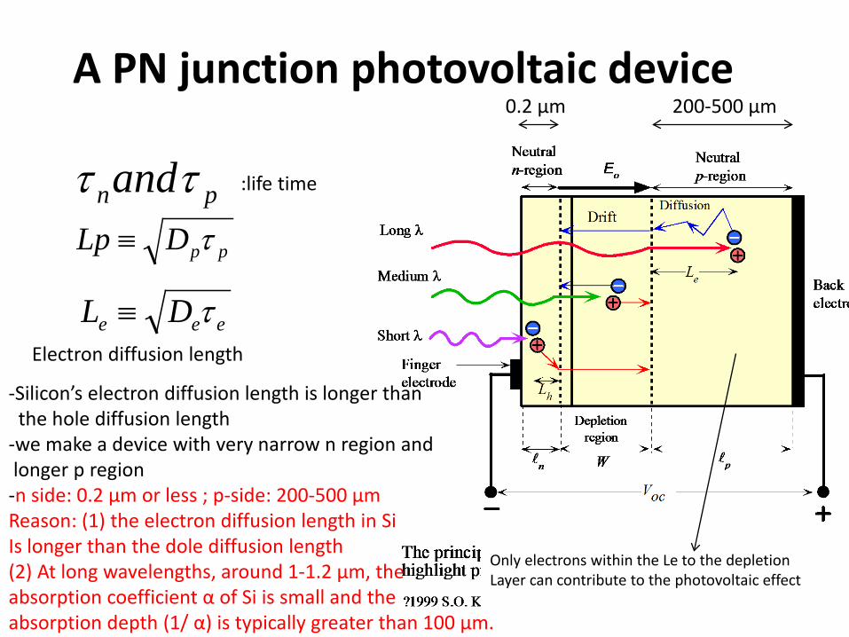
A PN junction photovoltaic device
-incoming photon generate EHPs and separated by the build-in field Eo, drifts them apart -generated electrons and hole can diffuse and drift in neural region and SCL, respectively -
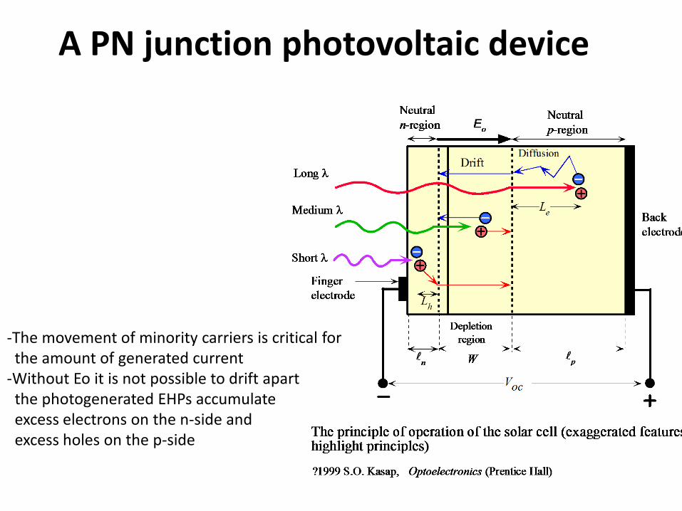
A PN junction photovoltaic device
-The movement of minority carriers is critical for the amount of generated current -Without Eo it is not possible to drift apart the photogenerated EHPs accumulate excess electrons on the n-side and excess holes on the p-side
A PN junction photovoltaic device
pnandττppDLp τ≡
eee DL τ≡
:life time
Only electrons within the Le to the depletion Layer can contribute to the photovoltaic effect
-Silicon’s electron diffusion length is longer than the hole diffusion length -we make a device with very narrow n region and longer p region -n side: 0.2 μm or less ; p-side: 200-500 μm Reason: (1) the electron diffusion length in Si Is longer than the dole diffusion length (2) At long wavelengths, around 1-1.2 μm, the absorption coefficient α of Si is small and the absorption depth (1/ α) is typically greater than 100 μm.
Electron diffusion length
200-500 μm 0.2 μm
LeLh W
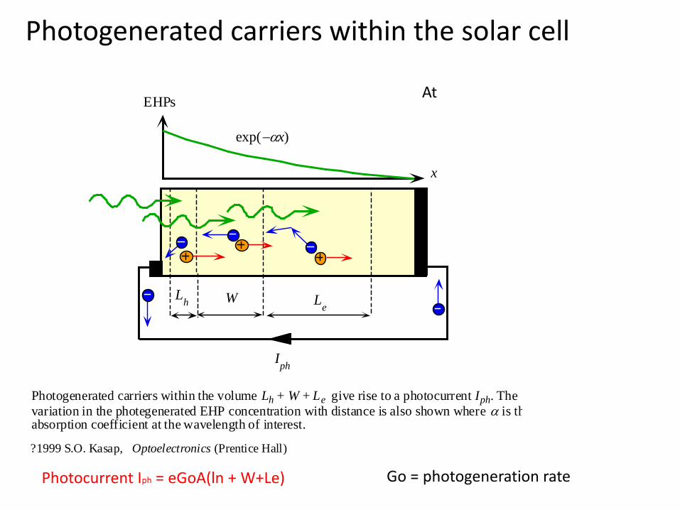
Iph
x
EHPs
exp(−αx)
Photogenerated carriers within the volume Lh + W + Le give rise to a photocurrent Iph. Thevariation in the photegenerated EHP concentration with distance is also shown where α is thabsorption coefficient at the wavelength of interest.
?1999 S.O. Kasap, Optoelectronics (Prentice Hall)
Photocurrent Iph = eGoA(ln + W+Le)
Photogenerated carriers within the solar cell
Go = photogeneration rate
At
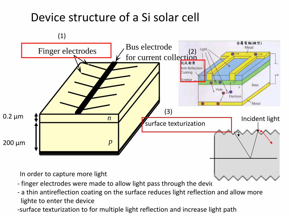
Device structure of a Si solar cell
and to allow more photons into the device
Finger electrodes
p
n
Bus electrode for current collection
- finger electrodes were made to allow light pass through the device - a thin antireflection coating on the surface reduces light reflection and allow more lighte to enter the device -surface texturization to for multiple light reflection and increase light path
0.2 μm
200 μm
In order to capture more light
surface texturization Incident light
(1)
(2)
(3)

Light trapped on texturization surface

The physics of antireflection

Device structure of a Si solar cell
and to allow more photons into the device
Finger electrodes
p
n
Bus electrode for current collection
- finger electrodes were made to allow light pass through the device - a thin antireflection coating on the surface reduces light reflection and allow more lighte to enter the device -surface texturization to for multiple light reflection and increase light path
0.2 μm
200 μm
In order to capture more light
surface texturization Incident light
(1)
(2)
(3)

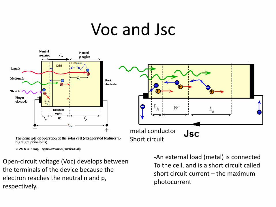
Open-circuit voltage (Voc) develops between the terminals of the device because the electron reaches the neutral n and p, respectively.
Voc and Jsc
metal conductor Short circuit
-An external load (metal) is connected To the cell, and is a short circuit called short circuit current – the maximum photocurrent
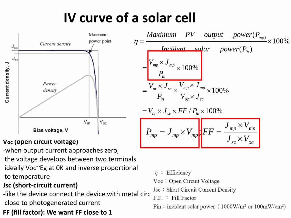
IV curve of a solar cell
Voc (open circuit voltage) -when output current approaches zero, the voltage develops between two terminals ideally Voc~Eg at 0K and inverse proportional to temperature Jsc (short-circuit current) -like the device connect the device with metal circuit, close to photogenerated current
ocsc
mpmpmpmpmp VJ
VJFFVJP
×
×=×= ;
%100/
%100
%100
%100)(
( )
×××=
××
××
×=
××
=
×=
inscoc
scoc
mpmp
in
scoc
in
mpmp
in
mp
PFFJV
JVJV
PJV
PJV
PpowersolarIncident
PpoweroutputPVMaximumη
FF (fill factor): We want FF close to 1
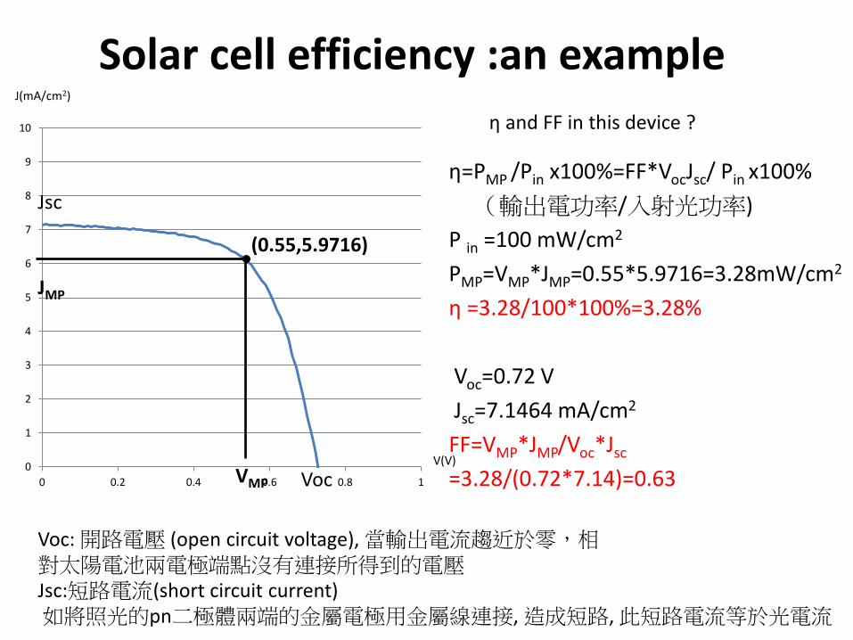
Solar cell efficiency :an example
0
1
2
3
4
5
6
7
8
9
10
0 0.2 0.4 0.6 0.8 1
J(mA/cm2)
V(V)
η=PMP /Pin x100%=FF*VocJsc/ Pin x100% (輸出電功率/入射光功率) P in =100 mW/cm2
PMP=VMP*JMP=0.55*5.9716=3.28mW/cm2 η =3.28/100*100%=3.28% Voc=0.72 V Jsc=7.1464 mA/cm2 FF=VMP*JMP/Voc*Jsc =3.28/(0.72*7.14)=0.63
(0.55,5.9716)
VMP
JMP
Voc
Jsc
Voc: 開路電壓 (open circuit voltage), 當輸出電流趨近於零,相 對太陽電池兩電極端點沒有連接所得到的電壓 Jsc:短路電流(short circuit current) 如將照光的pn二極體兩端的金屬電極用金屬線連接, 造成短路, 此短路電流等於光電流
η and FF in this device ?

Theoretical efficiency limit

100% Incident radiation
× 0.74 Insufficient photon energyhυ < Eg
× 0.59
Excessive photon energyNear surface EHP recombinationhυ > Eg
× 0.95 Collection efficiency of photons
× 0.6 Voc ≈ (0.6Eg)/(ekB)
× 0.85
η ≈ 21%
FF ≈ 0.85
Overall efficiency
Accounting for various losses of energy in a high efficiency Sisolar cell. Adapted from C. Hu and R. M. White, Solar Cells(McGraw-Hill Inc, New York, 1983, Figure 3.17, p. 61).?1999 S.O. Kasap, Optoelectronics (Prentice Hall)
Various losses of solar energy of a Si solar cell during processing
Silicon band gap is 1.1 eV, and the device loses all photon energy less than 1.1 eV
Voc is inverse proportional to temperature, so not equals to Eg
Only 43.6% remaining! - Excessive photon energy loss -Crystal surfaces and interfaces Contain a high concentration of Recombination centers Antireflection coating is not perfect
The highest efficient of a real photovoltaic device that uses a single crystal of Si Is about 24.7% (澳洲新南威爾斯 大學)
device fabrication resistance
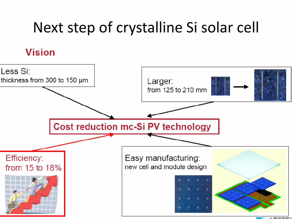
Next step of crystalline Si solar cell
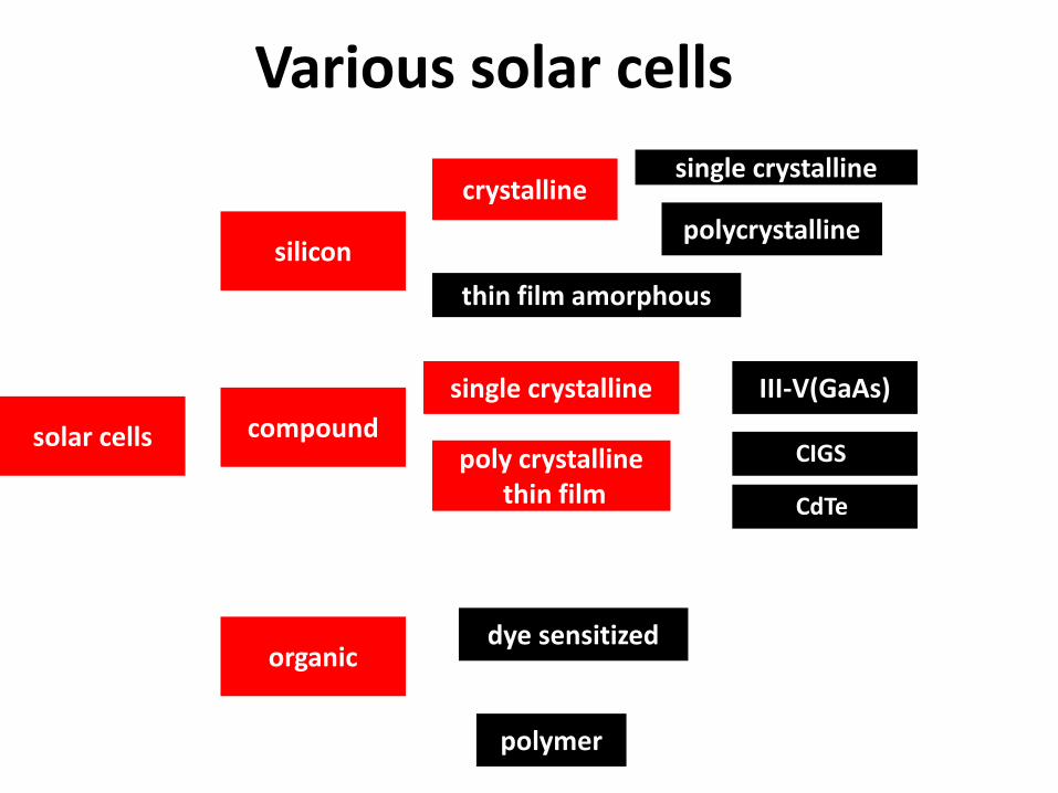
Various solar cells
solar cells
silicon
compound
organic
crystalline
thin film amorphous
single crystalline
polycrystalline
III-V(GaAs)
poly crystalline thin film
dye sensitized
polymer
single crystalline
CIGS
CdTe
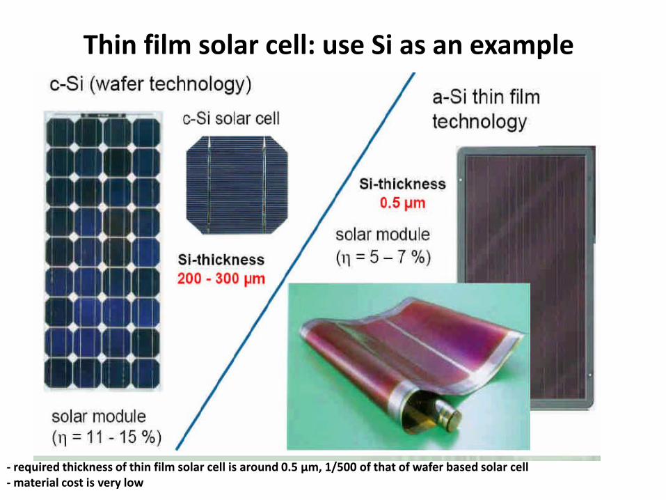
Thin film solar cell: use Si as an example
- required thickness of thin film solar cell is around 0.5 μm, 1/500 of that of wafer based solar cell - material cost is very low

Photovoltaic materials and their cell ηcomparison High Cost Thin film solar cell
Materials s-Si or poly Si
a-Si CdTe CIGS
manufacturing process
Crystal growth
PECVD Sublimation Evaporation/selenization
Cell efficiency
21% 13% 16% 19.9%
Potential for production cost <$1.00/Watt
Doubtful Fair Good Very good
Flexible modules
No Yes No (rigid packing)
Yes
Stability Very good Intrinsic degradation
Contact degradation
No known degradation
Remarks Shortage of raw Si wafer
manufactruing is xpensive -poor materials utilization
Borderline efficienci after decades
Need non-vaccum process for low lost production

Advantages of thin film solar cells
1. low raw materials are required for fabrication
2. light transmission is better
3. more competitive price (CdTe, US$1 per watt ; First Solar, stock price is US$180 )
4. frameless design
5. Ideal for BIPV( building integrated photovoltaic)

(very short)
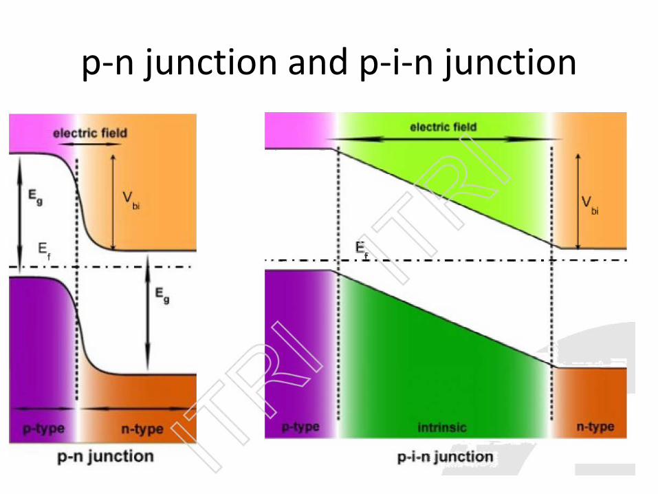
p-n junction and p-i-n junction
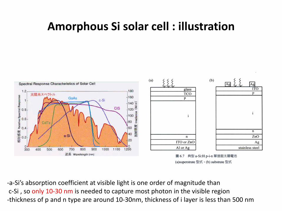
Amorphous Si solar cell : illustration
-a-Si’s absorption coefficient at visible light is one order of magnitude than c-Si , so only 10-30 nm is needed to capture most photon in the visible region -thickness of p and n type are around 10-30nm, thickness of i layer is less than 500 nm
圖6.7

CVD

II-VI compound solar cell: CdTe
Abbreviated periodic table I II III IV V VI B C N O Al Si P S Cu Zn Ga Ge As Se Ag Cd In Sn Sb Te
II-VI group as light harvesting materials
band gap of CdTe : 1.5 eV

Device structure of CdTe solar cell
P-type: CdTe n-type: CdS

First solar: CdTe solar cells
2010年全世界生產成本最低的太陽能電池模組公司
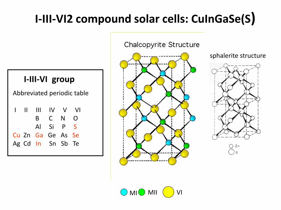
I-III-VI group
sphalerite structure
Abbreviated periodic table I II III IV V VI B C N O Al Si P S Cu Zn Ga Ge As Se Ag Cd In Sn Sb Te
VI MI MII
I-III-VI2 compound solar cells: CuInGaSe(S)
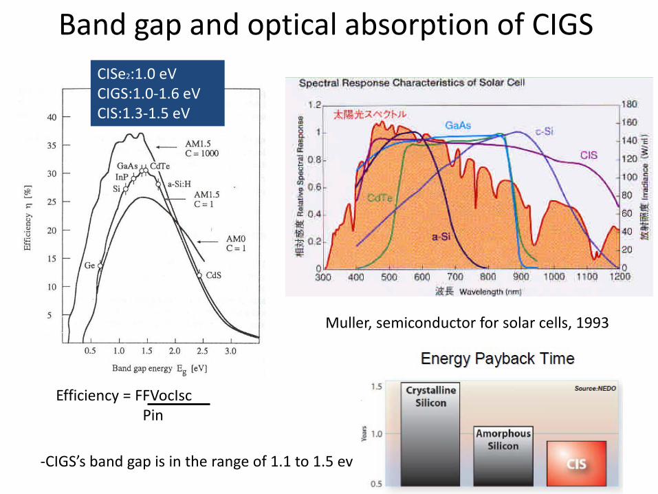
Band gap and optical absorption of CIGS
Muller, semiconductor for solar cells, 1993
CISe2:1.0 eV CIGS:1.0-1.6 eV CIS:1.3-1.5 eV
-CIGS’s band gap is in the range of 1.1 to 1.5 ev
Efficiency = FFVocIsc Pin
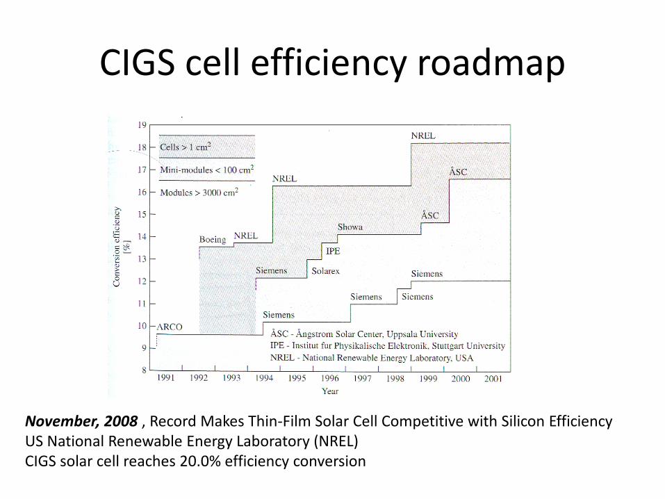
CIGS cell efficiency roadmap
November, 2008 , Record Makes Thin-Film Solar Cell Competitive with Silicon Efficiency US National Renewable Energy Laboratory (NREL) CIGS solar cell reaches 20.0% efficiency conversion
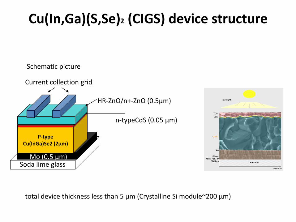
Cu(In,Ga)(S,Se)2 (CIGS) device structure
P-type Cu(InGa)Se2 (2µm)
Soda lime glass Mo (0.5 µm)
n-typeCdS (0.05 µm)
HR-ZnO/n+-ZnO (0.5µm)
Current collection grid
total device thickness less than 5 µm (Crystalline Si module~200 µm)
Schematic picture

Vacuum-based techniques for CIGS film deposition
Drawbacks: -difficult to achieve controlled-stoichiometry over large device areas -manufacturing equipment is “very” expensive (> NT 0.1 billion) -the deposition process is time-consuming -low materials utilization (30-50%) -low throughput
Heater and substrate
Evaporation sources
CIGS film deposition method: Multistage coevaporation process in a vacuum chamber
-Highest efficiency (lab scale: 18~20%) -Usually UHV/MBE -Cost prohibitive (but <cryst-Si)

59
Non-Vacuum Processing
-Synthesize colloidal nanocrystals with controlled CIGS stoichiometry and deposit layer -Roll-to-roll manufractruing process

ISET’s non-vacuum process
60 Kapur V.K. thin solid film, 2003
Substrate Efficiency Air Mass
Soda lime Glass 13.6% AM 1.5
Molybdenum Foil
13.0% AM 1.5
Titanium foil 9.5% AM 1.5
Polyimide film 10.4% AM 1.5
Stainless Stell 9.6% AM 1.5

Nanosolar。破產,2013年7月

CIGS Rocks!
【時報記者沈培華台北報導】台積電 (2330) 新事業總經理蔡力行表示, 台積電將以CIGS薄膜產品進軍太陽能產業,以五年期間朝全球前五大廠邁進, 產能規模將達1GW規模,並看好此事業對台積電是有獲利與高成長潛力的新事業。 台積電今天舉行先進薄膜太陽能技術研發中心暨先期量產廠房動土典禮。 新事業總經理蔡力行表示,全球太陽能電池市場將持續成長,預期2009年至 2015年全球太陽能電池市場年複合成長率可望達23%;其中,銅銦鎵硒(CIGS) 因具有薄膜的低成本價格等優勢,成長率將最高,年複合成長率將達115%。 台積電因此將以CIGS薄膜產品為主力,進軍太陽能產業。 台積電先進薄膜太陽能廠第一期將投資約79.2億,預計2012年量產200百萬瓦(MW) ,終期產能為700百萬瓦(MW)。台積電董事長張忠謀並預估,2015年太陽能佔 台積電營收比重可望達10%。蔡力行表示,台積電三年內CIGS薄膜太陽能電池 模組轉換效率將達14%,產能規模將約300至500百萬瓦,預期3至5年轉換效率 將進一步提升至16%,產能規模將達1GW規模。
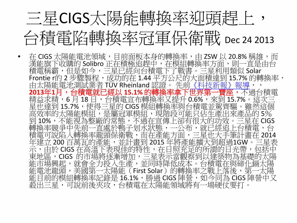
三星CIGS太陽能轉換率迎頭趕上,台積電陷轉換率冠軍保衛戰 Dec 24 2013
• 在 CIGS 太陽能電池領域,目前面板本身的轉換率,由 ZSW 以 20.8% 稱雄,而漢能旗下收購的 Solibro 正在積極追趕中,在模組轉換率方面,則一直是由台積電稱霸,但是如今,三星已經向台積電下了戰書。三星利用類似 Solar Frontie r的 2 步驟製程,成功的在 1.44 平方公尺的大面積達到 15.7% 的轉換率,由太陽能電池測試業者 TÜV Rheinland 認證。 先前《科技新報》報導,,2013年1月,台積電就已經以 15.1% 的轉換率拿下世界第一寶座,不過台積電精益求精,6 月 18 日,台積電宣布轉換率又提升 0.6%,來到 15.7%。這次三星也達到 15.7%,使得三星的 CIGS 模組轉換率與台積電並駕齊驅。雖然這個高效率的太陽能模組,是屬冠軍模組,現階段可能只佔生產出來產品的 5% 到 10%,不能視為整廠的常態,不過在宣傳上卻有很大的功效。三星在 CIGS 轉換率競爭中先前一直處於鴨子划水狀態,一公布,就已經追上台積電,台積電可說陷入轉換率龍頭保衛戰,而在產能方面,三星也大手筆計畫在 2014 年建立 200 百萬瓦的產能,並計畫到 2015 年將產能擴大到超過1GW。三星表示,由於 CIGS 在高溫下表現佳的特性,在日照充足的所謂的日光帶,包括中東地區,CIGS 的市場將逐漸增加,三星表示當觀察到以建築物為基礎的太陽能市場興起,就會全力投入生產,並同時降低成本。台積電在與碲化鎘太陽能電池龍頭,美國第一太陽能(First Solar)的轉換率之戰上落後,第一太陽能目前的模組轉換率記錄是 16.1%,勝過 CIGS 陣營,如今同為 CIGS 陣營中又殺出三星,可說前後夾攻,台積電在太陽能領域將有一場硬仗要打。

Silicon Wafer cells
Vacuum-based thin film
Roll-printed thin film
Process Si wafer processing
High vacuum depositon
Roll-to-roll printing
Process Yield
Robust Fragile Robust
Materials Utilization
30% 30-60% Over 97%
Throughput 1 2-5 10-25
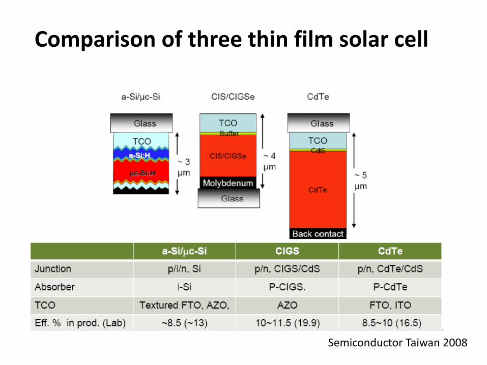
Comparison of three thin film solar cell
Semiconductor Taiwan 2008
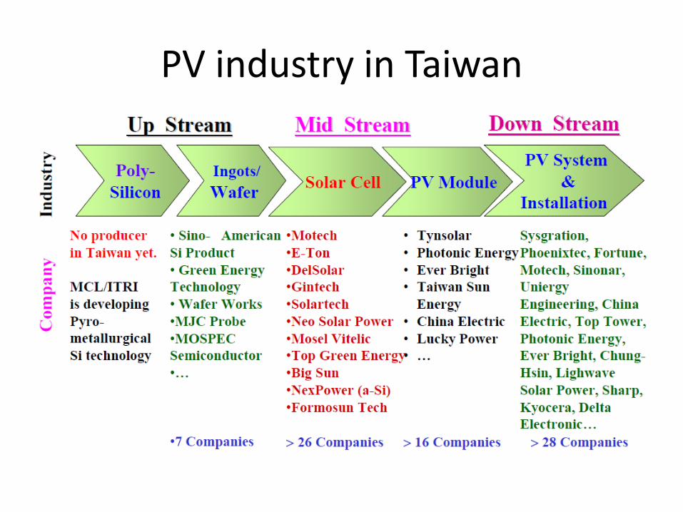
PV industry in Taiwan
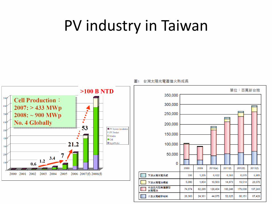
PV industry in Taiwan

Market distribution in 2009