memory synthesis for fpga implementation of real-time video processing systems
TRANSCRIPT

Thesis for the degree of Doctor of Technology Sundsvall 2008
Memory Synthesis for FPGA Implementation of Real-Time Video Processing Systems
Najeem Lawal
Supervisors: Professor Mattias O’Nils Professor Bengt Oelmann Doctor Benny Thörnberg
Electronics Design Division, in the
Department of Information Technology and Media Mid Sweden University, SE-851 70 Sundsvall, Sweden
ISSN 1652-893X Mid Sweden University Doctoral Thesis 66
ISBN 978-91-86073-26-8
Akademisk avhandling som med tillstånd av Mittuniversitetet i Sundsvall framläggs till offentlig granskning för avläggande av teknologie doktors examen i elektronik onsdagen den 07 Jan 2009, klockan 10:30 i sal O102, Mittuniversitetet Sundsvall. Seminariet kommer att hållas på engelska. Memory Synthesis for FPGA Implementation of Real-Time Video Processing Systems Najeem Lawal © Najeem Lawal, 2009
Electronics Design Division, in the Department of Information Technology and Media Mid Sweden University, SE-851 70 Sundsvall Sweden Telephone: +46 (0)60 148561
Printed by Kopieringen Mittuniversitetet, Sundsvall, Sweden, 2009

iii
ABSTRACT
In this thesis, both a method and a tool to enable efficient memory synthesis for real-time video processing systems on field programmable logic array are presented. In real-time video processing system (RTVPS), a set of operations are repetitively performed on every image frame in a video stream. These operations are usually computationally intensive and, depending on the video resolution, can also be very data transfer dominated. These operations, which often require data from several consecutive frames and many rows of data within each frame, must be performed accurately and under real-time constraints as the results greatly affect the accuracy of application. Application domains of these systems include machine vision, object recognition and tracking, visual enhancement and surveillance.
Developments in field programmable gate arrays (FPGAs) have been the motivation for choosing them as the platform for implementing RTVPS. Essential logic resources required in RTVPS operations are currently available and are optimized and embedded in modern FPGAs. One such resource is the embedded memory used for data buffering during real-time video processing. Each data buffer corresponds to a row of pixels in a video frame, which is allocated using a synthesis tool that performs the mapping of buffers to embedded memories. This approach has been investigated and proven to be inefficient. An efficient alternative employing resource sharing and allocation width pipelining will be discussed in this thesis.
A method for the optimised use of these embedded memories and, additionally, a tool supporting automatic generation of hardware descriptions language (HDL) modules for the synthesis of the memories according to the developed method are the main focus of this thesis. This method consists of the memory architecture, allocation and addressing. The central objective of this method is the optimised use of embedded memories in the process of buffering data on-chip for an RVTPS operation. The developed software tool is an environment for generating HDL codes implementing the memory sub-components.
The tool integrates with the Interface and Memory Modelling (IMEM) tools in such a way that the IMEM’s output - the memory requirements of a RTVPS - is imported and processed in order to generate the HDL codes. IMEM is based on the philosophy that the memory requirements of an RTVPS can be modelled and synthesized separately from the development of the core RTVPS algorithm thus freeing the designer to focus on the development of the algorithm while relying on IMEM for the implementation of memory sub-components.


v
SAMMANDRAG
I denna avhandling presenteras en metod och ett verktyg för möjliggörandet av effektiv minnessyntes för vidoebearbetande system i realtid på Field Programmable Gate Array (FPGA). I ett system som bearbetar video i realtid (RTVPS) upprepas en mängd processer i varje bildruta i en videosekvens. Dessa processer är ofta beräkningsintensiva och, beroende på videoupplösningen, kan de också vara mycket dataöverföringsstyrda. Processerna, som ofta kräver data från en mängd konsekutiva bildrutor och många dataserier inom varje ruta, måste genomföras exakt och under realtidsbegränsningar, då resultaten i hög grad påverkar tillämpningens exakthet. Tillämpningsområden för dessa system innefattar igenkänning av föremål, spårning av föremål samt övervakning.
Utvecklade produkter inom FPGA har motiverat användandet av dessa som plattform för tillämpning av RTVPS. De nödvändiga logikresurser som krävs för RTVPS-processer är för tillfället tillgängliga, optimerade och inbyggda i modern FPGA. En sådan resurs är det inbyggda minne som används för datalagring under videoprocessning i realtid. Varje datalager motsvarar en rad pixlar i en videoruta som automatiskt allokeras på FPGAs. Denna metod har undersökts och visat sig vara effektiv. Ett effektivt alternativ som utnyttjar resursdelning och anslag vid rörledning diskuteras i denna avhandling.
En metod för optimal användning av dessa inbäddade minnen och ett verktyg som stöder automatisk generering av HDL-koder för minnessyntes enligt den utvecklade metoden är fokus för denna avhandling. Denna metod består av minnesarkitektur, allokering och adressering. Metodens centrala mål är optimal användning av inbäddade minnen under lagring av data på chip för en RTVPS-operation. Den utvecklade mjukvaran är en miljö för att generera HDL-koder, där minneskomponenter tillämpas.
Verktyget integreras med IMEM-verktyg (Interface and Memory Modelling) på ett sådant sätt att IMEM:s utdata – minneskraven för ett RTVPS, importeras och behandlas för att generera HDL-koderna. IMEM baseras på filosofin att minneskraven för ett RTVPS kan modelleras och syntetiseras separat från utvecklandet av den ursprungliga huvudalgoritmen för RTVPS och därigenom ge designern frihet att fokusera på utvecklingen av algoritmen, medan IMEM används för tillämpning av minneskomponenter.

vii
ACKNOWLEDGEMENTS
First of all I would like to show my great appreciation of my supervisors Prof. Mattias O’Nils, Prof. Bengt Oelmann and Dr. Benny Thörnberg for their academic and scientific guidance and inspirations, and for giving me the opportunity to study for Ph.D. Prof. Hans-Erik Nilsson and Dr. Jerzy Kirrander are greatly acknowledged for their contributions and inspirations. I am grateful to Fanny Burman and Lotta Söderström for their kind support. I would also like to thank all my colleagues at the Mid Sweden University, my friends and my family for their supports.
I would also like to express my gratitude to the Mid Sweden Unviersity,
the Swedish KK foundation and ARTES Graduate School for their financial supports.
Sundsvall, Jan 2009
Najeem Lawal


ix
TABLE OF CONTENTS
ABSTRACT ............................................................................................................. III
SAMMANDRAG .......................................................................................................V
ACKNOWLEDGEMENTS.......................................................................................VII
TABLE OF CONTENTS ..........................................................................................IX
ABBREVIATIONS AND ACRONYMS ..................................................................XIII
LIST OF FIGURES ................................................................................................ XV
LIST OF TABLES ................................................................................................ XVII
LIST OF PAPERS................................................................................................. XIX
1 INTRODUCTION...............................................................................................1 1.1 REAL-TIME VIDEO PROCESSING SYSTEM.............................................. 1 1.2 IMPLEMENTATION ALTERNATIVES ......................................................... 4
1.2.1 Application Specific Integrated Circuits..................................... 4 1.2.2 Software Based Processors...................................................... 4 1.2.3 Programmable Hardware Processors....................................... 4
1.3 DATA REQUIREMENTS IN RTVPS......................................................... 6 1.4 MOTIVATION FOR EFFICIENT MEMORY SYNTHESIS ................................ 9 1.5 PROBLEM DESCRIPTION..................................................................... 10 1.6 PERFORMANCE COMPARISON ............................................................ 11
1.6.1 Experimental Set-Up ............................................................... 11 1.6.2 Results .................................................................................... 12 1.6.3 Conclusion............................................................................... 13
1.7 MAIN CONTRIBUTIONS ....................................................................... 14 1.8 THESIS OUTLINE................................................................................ 14
2 FIELD PROGRAMMABLE GATE ARRAY (FPGA) .......................................15 2.1.1 Programmable Logic Cells ...................................................... 15 2.1.2 Programmable Interconnects .................................................. 17 2.1.3 On-chip RAM Block................................................................. 19 2.1.4 Embedded cores ..................................................................... 19
3 RELATED WORKS.........................................................................................21 3.1 CHALLENGES IN SYSTEM DEVELOPMENT ON FPGA ............................. 21
3.1.1 Abstraction level ...................................................................... 21 3.1.2 Design verification................................................................... 22 3.1.3 Resource usage ...................................................................... 22 3.1.4 Energy and power consumption.............................................. 22
x
3.2 DESIGN METHODS AND LANGUAGES ...................................................23 3.2.1 C/C++ Models..........................................................................23 3.2.2 Java Model ..............................................................................24 3.2.3 MATLAB Model .......................................................................24 3.2.4 Hardware Description Model ...................................................25 3.2.5 Performance comparison ........................................................25
3.3 PREVIOUS WORKS ON ON-CHIP MEMORY SYNTHESIS.........................26 3.3.1 Allocation algorithms ...............................................................26 3.3.2 Memory addressing .................................................................27 3.3.3 C++ based System Synthesis .................................................28 3.3.4 Constraint Generation .............................................................29 3.3.5 Response to related works ......................................................29
4 MEMORY SYNTHESIS FOR REAL-TIME VIDEO PROCESSING SYSTEMS........................................................................................................31
4.1 IMEM SYNTHESIS WORKFLOW...........................................................31 4.2 TOOL INTEGRATION............................................................................33
4.2.1 Integration with C-Based tools.................................................33 4.2.2 Integration with MATLAB.........................................................34 4.2.3 Integration with Xilinx ISE and ModelSim................................34
4.3 MEMORY SYNTHESIS ARCHITECTURE .................................................34 4.4 MEMORY IMPLEMENTATION ................................................................37 4.5 MEMORY ALLOCATION........................................................................38
4.5.1 Allocation algorithm .................................................................38 4.5.2 Definitions................................................................................39 4.5.3 Proposed algorithm .................................................................42 4.5.4 Complexity analysis.................................................................43
4.6 ARCHITECTURE DRIVEN BLOCK RAM OPTIMISATION ...........................43 4.7 MEMORY ACCESSING.........................................................................46
4.7.1 Base Pointer Approach............................................................47 4.7.2 Distributed Pointer Approach...................................................48
4.8 CONSTRAINT GENERATION.................................................................49 4.9 RESULTS...........................................................................................53
4.9.1 Real-time video processing design cases ...............................53 4.9.2 Allocation Results ....................................................................54 4.9.3 Performance analysis with varying length and width ..............56 4.9.4 Performance analysis with varying length and Block RAM sizes 59 4.9.5 Performance Analysis for video processing systems..............60 4.9.6 Performance of Architecture Driven Memory Allocation .........62 4.9.7 Results of the addressing........................................................63 4.9.8 Result of Constraint Generation ..............................................64
5 PAPERS SUMMARY ......................................................................................67 5.1 MEMORY SYNTHESIS .........................................................................68
5.1.1 Paper I .....................................................................................68 5.1.2 Paper VII..................................................................................68 5.1.3 Paper II ....................................................................................68
5.2 PERFORMANCE ANALYSIS ..................................................................68
xi
5.2.1 Paper III................................................................................... 68 5.2.2 Paper IV .................................................................................. 69
5.3 TOOLS INTEGRATION ......................................................................... 69 5.3.1 Paper V ................................................................................... 69
5.4 POST-SYNTHESIS OPTIMISATION........................................................ 69 5.4.1 Paper VI .................................................................................. 69
5.5 AUTHORS CONTRIBUTIONS................................................................. 70 6 THESIS SUMMARY........................................................................................71
6.1 DISCUSSIONS .................................................................................... 71 6.1.1 Memory architecture ............................................................... 71 6.1.2 Memory allocation ................................................................... 72 6.1.3 Memory addressing................................................................. 72 6.1.4 Boundary conditions management.......................................... 72 6.1.5 IMEM interfaces ...................................................................... 72 6.1.6 Constraint Generation ............................................................. 73
6.2 CONCLUSIONS................................................................................... 73 6.3 FUTURE WORKS................................................................................ 74
7 REFERENCE ..................................................................................................75
APPENDIX A ..........................................................................................................81
PAPER I ..................................................................................................................83
PAPER II ...............................................................................................................107
PAPER III ..............................................................................................................115
PAPER IV..............................................................................................................121
PAPER V...............................................................................................................131
PAPER VI..............................................................................................................141
PAPER VII.............................................................................................................149


xiii
ABBREVIATIONS AND ACRONYMS
ALU ............. Arithmetic Logic Unit ASIC ............. Application Specific Integrated Circuit ASIP ............. Application Specific Instruction set Processor BRAM ………... Block RAM CAD ............. Computer Aided Design CLB ............. Configurable Logic Block CPLD ............. Complex PLD CPU ............. Central Processing Unit DCM ............. Digital Clock Manager DRAM ............. Dynamic RAM DSP ............. Digital Signal Processing FIFO ............. First In First Out FIR ............. Finite Inpulse Response FPGA ............. Field Programmble Gate Array GMO ............. Global Memory Object GPP ............. General Purpose Processor HDL ............. Hardware Description Language HDTV ............. High-Definition Television HLL ............. High Level programming Language IIR ............. Infinte Impulse Ressponse IMEM ............. Interface and Memory Modeling IP ............. Intellectual Property IOB ............. Input/Output Block LUT ............. Look Up Table MMX ............. Multimedia Extension PLD ............. Programmble Logic Device RAM ............. Random Access Memory RISC ............. Reduced Instruction Set Computer RTL ............. Register Transfer Level RTVPS ............. Real-Time Video Processing System SIMD ……….. Single Instruction Multiple Datapath SLWC ............. Sliding Window Controller SRAM ............. Static RAM UML ............. Unified Modelling Language VHDL ............. VHSIC HDL VHSIC ............. Very-High-Speed Integrated Circuits VIP ............. Video/Image Processing VLIW ............. Very Large Instruction Word VLSI ............. Very Large Scale Integration

xiv

xv
LIST OF FIGURES
Figure 1. Improving visual appearance 2 Figure 2. Preparing for feature measurement 2 Figure 3. Video processing system 3 Figure 4. Time-to-Market - FPGAs vs. ASICs [14] 5 Figure 5. Product time-in-market [14] 5 Figure 6. Signal processing implementation spectrum [15]. 6 Figure 7. Comparison of various implementation platforms [8] 6 Figure 8. Neighbourhood oriented image processing 7 Figure 9. Spatial temporal oriented image processing 8 Figure 10 Circular buffers as line buffers. 10 Figure 11 Block-RAM data flow at read first operation. 10 Figure 12 Resource usage on FPGA 12 Figure 13 Resource usage on DSP 13 Figure 14 Performance 13 Figure 15. Power consumption 13 Figure 16. Overview of Xilinx Spartan 3 [48] 16 Figure 17. Xilinx Spartan 3 CLB [48] 16 Figure 18. FPGA Interconnects 17 Figure 19. RAM data path [50] 19 Figure 20. Spartan 3 MicroBlaze embedded processor [54]. 20 Figure 21. Design Flow for implementing custom applications on FPGA 25 Figure 22. System synthesis workflow. 32 Figure 23 System integration and verification. 33 Figure 24. IMEM model of a video processing system. 35 Figure 25 A: Spatio-temporal neighbourhood of pixels. B: Memory architecture
for a single image processing operation. 35 Figure 26 Boundary conditions implementation architecture. 36 Figure 27 Neighbourhood oriented system. 36 Figure 28 Global Memory Object formation 37 Figure 29. Traditional memory allocation. 38 Figure 30. Proposed memory allocation. 39 Figure 31. Partitioning global memory object. 41 Figure 32. Allocation model. 42 Figure 33. The proposed allocation algorithm. 42 Figure 34 Architecture driven memory allocation 46 Figure 35 Two memory accessing approaches 47 Figure 36. Base Pointer Approach. 48 Figure 37. Distributed Approach. 49 Figure 38. Constraint generation algorithm 52 Figure 39. Clock distributions showing the effect of constraints 52 Figure 40. Constraint generation workflow 53 Figure 41. Memory allocation of Case 2-1 on Xilinx Spartan 2E FPGA. 56 Figure 42a. First test scenario on Spartan 2E. 57 Figure 43a. Second test scenario on Spartan 2E. 58

xvi
Figure 44. Block RAM usage with varying memory requirements 60 Figure 45. Memory usage 63 Figure 46. Post-PAR Clock distribution of design case 2 63 Figure 47. Relationship between thesis papers. 67

xvii
LIST OF TABLES
Table 1. Summary of FPGA inter-connects .................................................... 18 Table 2. Memory requirement of considered design cases. ........................... 54 Table 3. Allocation result of the algorithm on Spartan 2E............................... 54 Table 4. Allocation result of the algorithm on Spartan 3. ................................ 54 Table 5.Average allocation results for all cases ............................................. 61 Table 6. Allocation on Spartan II ..................................................................... 61 Table 7. Allocation on Spartan III .................................................................... 61 Table 8. Comparison of the two approaches. ................................................. 63 Table 9. Resource usage summary ................................................................ 65 Table 10. Dynamic power consumption.......................................................... 66 Table 11. Authors’ Contributions..................................................................... 70


xix
LIST OF PAPERS
This thesis is mainly based on the following five papers, herein referred to by their Roman numerals:
Paper I
RAM Allocation Algorithm for Video Processing Applications on FPGA, Najeem Lawal, Benny Thörnberg, Mattias O’Nils and Håkan Norell, Accepted for publication in Journal of Circuits, Systems and Computers., Vol. 15, No. 5, October 2006.
Paper II Address Generation for FPGA RAMs for Efficient
Implementation of Real-Time Video Processing Systems, N. Lawal, B. Thörnberg, M. O'Nils, Proceedings of the Conference on Field Programmable Logic and Applications, Tampere, Finland, 2005, pp. 136 - 141. ISBN 0-7803-9362-7
Paper III Embedded FPGA Memory Requirements for Real-Time Video
Processing Applications Najeem Lawal and Mattias O'Nils, Proceedings of the 23rd Norchip Conference, Oulu, Finland November 2005, pp. 206 - 209. ISBN 1-4244-0064-3
Paper IV Automatic Generation of Spatial and Temporal Memory
Architectures for Embedded Video Processing Systems, H. Norell, N. Lawal and M. O’Nils, In European Association for Signal and Image Processing (EURASIP) Journal on Embedded Systems, Volume 2007, 2007.
Paper V C++ based System Synthesis of Real-Time Video Processing
Systems targeting FPGA Implementation, N. Lawal, B. Thörnberg and M. O’Nils, Proceeding of the 21th International Parallel and Distributed Processing Symposium (IPDPS 2007), 26-30 March 2007, Long Beach, California, USA.
Paper VI Power-aware Automatic Constraint Generation for FPGA
Based Real-Time Video Processing Systems N. Lawal, B. Thörnberg and M. O’Nils, Proceedings of the 25th IEEE Norchip Conference, Aalborg Denmark November 2007, pp. 1 - 5. ISBN: 978-1-4244-1516-8

xx
Paper VII Architecture driven memory allocation for FPGA Based Real-Time Video Processing Systems N. Lawal, B. Thörnberg and M. O’Nils, Submitted to Journal of Embedded Hardware Design.
Related papers not included into this thesis:
Evaluation of embedded RAM characteristics for FPGA implementation of real-time image processing systems, J. Rojas, N. Lawal and M. O'Nils, Study report
Comparison of FPGA and DSP performances in
neighbourhood oriented real-time video processing Najeem Lawal, Study report
C++ based System Synthesis of Real-Time Video Processing
Systems targeting FPGA Implementation, M. O'Nils, B. Thörnberg and N. Lawal, In Proceeding of FPGAworld Conference, Nov 2007.

1
1 INTRODUCTION
This thesis is concerned with memory synthesis in the implementation of real-time video processing systems on field programmable gate arrays. This memory synthesis considers memory architecture, allocation, accessing, power optimisation and constraint generation. Our interest in memory synthesis is to provide an easy to use high-level design tool for managing the data required in real-time video processing systems. This interest originates from the fact that implementing memory for required data is extremely taxing, the available memory is limited and the current memory synthesis methodologies do not offer a cost-effective use of the limited memory. To present this thesis, we will first present the essential background to a real-time video processing system in Section 1.1. Section 1.2 presents four alternatives for implementing real-time video processing systems. In Section 1.3 we will identify sources for the data requirement in video processing and the motivation behind this work. We present the contribution of this thesis in Section 1.4. Finally, in Section 1.5 we will present the outline of this thesis.
1.1 REAL-TIME VIDEO PROCESSING SYSTEM
Images represent an important part of information communication in everyday life. They are essential parts of the interaction between people, human-computer interaction and computer computation. Images are useful in reasoning, education, communication, navigation and analysis. Image processing can be described as a task which converts an input image into a modified output image or a task that extract information from the features present in an image. Image processing is used for two somewhat different purposes namely:
1. improving the visual appearance of images to the human viewer 2. preparing images for the measurement of the features and the
structures present Because these two purposes are different, the operations involved in them
might also be different, but they do share many common operations. In general the

2
purpose of image processing is not to reduce data content (which might often be case when images are transformed from colour images to gray-scale images or from gray-scale images to binary) but to preserve and magnify the quality of the image. For visual enhancement, operations that facilitate human comprehension and that make images subjectively appealing are carried out. Examples of these operations include contrast adjustment, image smoothening and colourisation. The operations are useful in video entertainment, image printing, transmission and reproduction. Figure 1 shows different operations that can be applied to an original image (A) to make it visually appealing and comprehensible.
In image measurement, operations that cause the image features to be well defined and more pronounced through enhanced edges or uniform brightness for objective analysis and classification are carried-out. Examples of these operations include image segmentation, noise elimination and morphological erosion and dilation. These operations find applications in robot vision and machine vision. Figure 2 shows operations that can be applied to an input image to make the counting of the features in the image easier and autonomous by a computer.
(A) (B) (C) (D)
Figure 1. Improving visual appearance
(A) (B) (C) (D)
Figure 2. Preparing for feature measurement
The effectiveness of image processing operations affect the complexity of the subsequent stages of image usage such as image compression and de-compression, image storage and retrieval and, image transmission. Thus image processing operations will continue to play a major role in the hand-held, battery-power mobile devices for video conferencing, video telephony and robot vision. This is because an excellently processed, feature enhanced and error free image will

3
greatly simplify a coding algorithm and provide better use of storage spaces and transmission bandwidth.
Video processing is essentially image processing in which the time domain is considered. This means that it might be necessary to register and process temporal changes in the image content. Figure 3A shows a typical set-up of a video processing system. The set-up includes an image acquisition device (the camera), the image processing unit (the processor) and an information consumption unit (the display). Of course, it is possible to have other components such as light sources, storage devices, human observers and communication devices based on applications. We will however focus on the essential aspects of image processing. Figure 3B shows the relationship between a single picture element (pixel) and an image whereas Figure 3C depicts the relationship between images and video. At the lowest level of operation, video processing involves the processing of each pixel in an image and image after image through-out the video stream.
(A)
Acquisition Processing Consumption
(B)
Valid Image Row
Image Pixel Clock
Image Pixel Data
Valid Image Data Image Blanking Image Blanking
...
...
...
...
P6 P0 P1 P2 P3 P4 P5 Pn-5 Pn-4 Pn-3 Pn-2 Pn-1
(C)
Image x Image x+1 Image x +2 Figure 3. Video processing system
Real-Time Video Processing System (RTVPS) is the term used to describe a
class of video processing system in which the video signal is processed at the rate of video capture such that the rate of generating output pixels matches the rate of receiving input pixels. Hence there is a throughput of one pixel per clock cycle. Thus after an initial delay, the system enters a state during which a pixel is being

4
received at the input side and, at the same time, a pixel is being produced at the output side. This does not, however, imply that this output pixel is the result of the newly received input pixel since there would be delays due to data buffering and pipelines in the computation.
1.2 IMPLEMENTATION ALTERNATIVES
In the following sub-sections, we will present four major alternatives for implementing RTVPS namely 1) general purpose processors, 2) application specific instruction-set processors, 3) field programmable gate arrays and 4) application specific integrated circuits. In general, implementation platforms can be classified as general purpose and applications specific from functionality point of view or they can be classified as reconfigurable or non-reconfigurable from programmability point of view.
1.2.1 Application Specific Integrated Circuits
Application Specific Integrated Circuits (ASICs) are fabricated and tailor-made for special or dedicated applications. This means that their precise functions and performance are considered and fully analyzed before fabrication. The consequence is efficiency, reliability and high performance. However, changes in system requirements which might be due to an oversight or a changing system demands results in a complete replacement of the device. In addition, unless market volume demand could really justify the manufacturing cost, the development costs for ASICs are a major set back. The trade-offs between performance and flexibility, which has an influence on the choice of computing devices, are presented in [1].
1.2.2 Software Based Processors
General Purpose Processors (GPPs) and Application Specific Instruction-set Processors (ASIPs) are software based and highly reconfigurable. On these devices application programs are written in high level languages and executed within a processor. Due to the sequential nature of these programs, large overheads are involved in the instruction set generation, decoding and execution. This limits the performance and throughput of these devices thus leading to the development of many instruction set architectures, which includes, VLIW, SIMD and MMX [2]. The main objective is for performance improvements through parallelism, pipelining, caching, and concurrency. The literature has much information with regards to the specifics of these architectures and since it is not the focus of the paper detailed discussions will not be provided.
1.2.3 Programmable Hardware Processors
In the hardware domain programmability can be achieved through the programmable gate-array or logic-devices which are commonly used. Depending
5
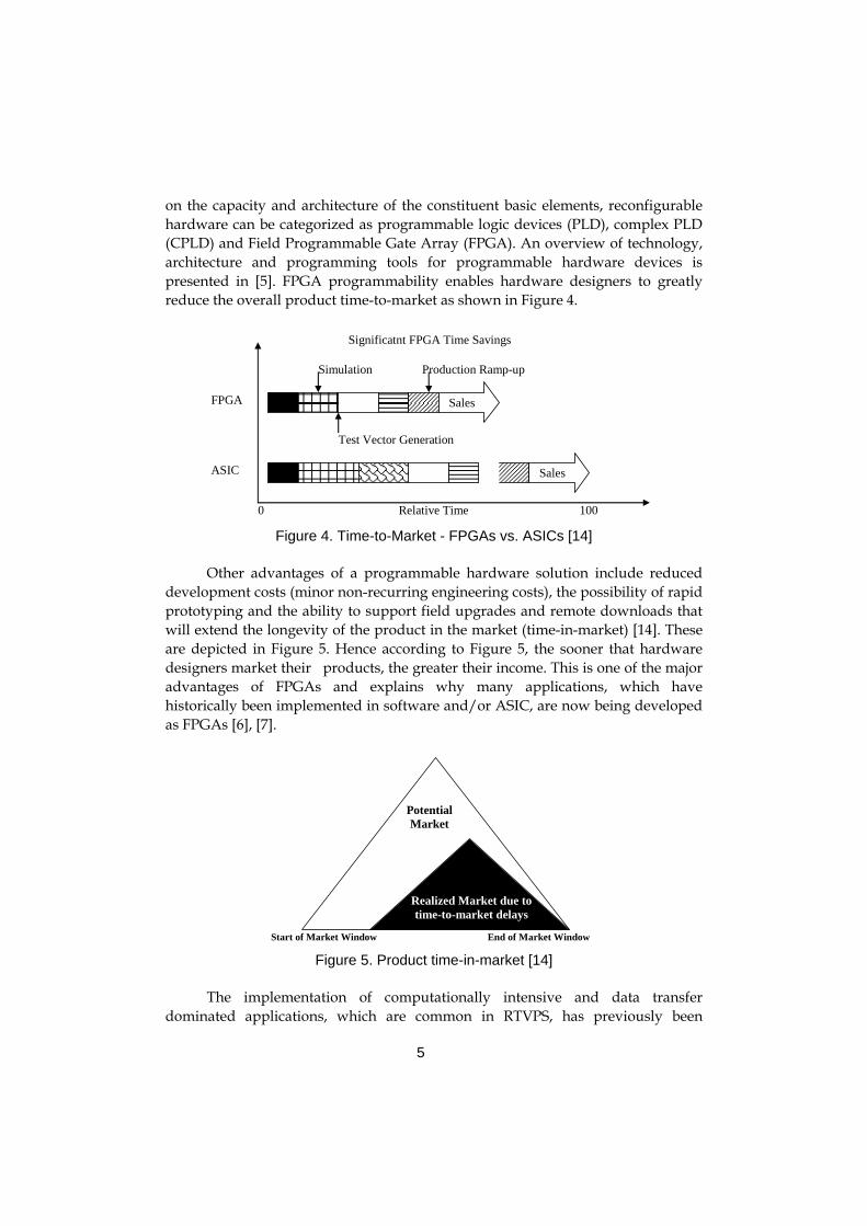
on the capacity and architecture of the constituent basic elements, reconfigurable hardware can be categorized as programmable logic devices (PLD), complex PLD (CPLD) and Field Programmable Gate Array (FPGA). An overview of technology, architecture and programming tools for programmable hardware devices is presented in [5]. FPGA programmability enables hardware designers to greatly reduce the overall product time-to-market as shown in Figure 4.
Relative Time
FPGA
ASIC
0 100
Significatnt FPGA Time Savings
Test Vector Generation
Production Ramp-up Simulation
Sales
Sales
Figure 4. Time-to-Market - FPGAs vs. ASICs [14]
Other advantages of a programmable hardware solution include reduced
development costs (minor non-recurring engineering costs), the possibility of rapid prototyping and the ability to support field upgrades and remote downloads that will extend the longevity of the product in the market (time-in-market) [14]. These are depicted in Figure 5. Hence according to Figure 5, the sooner that hardware designers market their products, the greater their income. This is one of the major advantages of FPGAs and explains why many applications, which have historically been implemented in software and/or ASIC, are now being developed as FPGAs [6], [7].
Start of Market Window End of Market Window
PotentialMarket
Realized Market due totime-to-market delays
Figure 5. Product time-in-market [14]
The implementation of computationally intensive and data transfer
dominated applications, which are common in RTVPS, has previously been

6
dominated by Digital Signal Processors (DSP) and dedicated application specific integrated circuits (ASIC). However, developments in FPGA have made it possible to implement RTVPS applications using FPGA [6], [7]. Figure 6 shows the implementation spectrum across computing devices. It should be noted that the different platforms in Figure 6 are not isolated as depicted in the figure but are over-lapping clouds. Figure 7 summaries the characteristics of the four platforms discussed above. From this comparison it is obvious that FPGA provides a reasonable performance alternative for image/video processing in real-time with the possibilities of re-programmability with evolving application specifications. For this reason FPGA has been chosen as the implementation platform for RTVPS. The following sections will focus on a detailed discussion on the FPGA technology.
General-Purpose Processor
Programmable DSP
ReconfigurableHardware
Specialization
Programmability
ASIC
Figure 6. Signal processing implementation spectrum [15].
F l e x i b i l i t y
Technology Performance / cost
Time to market
Time to change code functionality
Power Consumption
ASIC Very High Very Long Impossible Low
FPGA Medium – High
Long Long Low – Medium
ASIP Medium Medium Medium Medium – High
GPP Low – Medium
Very Short Very Short High
S p e e d
P e r f o rma n c e Figure 7. Comparison of various implementation platforms [8]
1.3 DATA REQUIREMENTS IN RTVPS
In this thesis introduction, we will not deal with discussions related to image acquisition such as lighting and optical set-up, image sampling and quantization. We will also not dwell on discussions regarding post processing and image

7
consumption such as monitor display, information reporting or decision making from the results of image processing. The stages as represented in Figure 3A are important to the core processing but are not included in the scope of this thesis. Our concern is with the operations involved in image processing and the need for data storage in image processing. We note that image processing can be carried out in two domains namely
1. spatial domain image processing 2. frequency domain image processing
Spatial domain depends on raw image pixel data and direct manipulation of
pixel whereas frequency domain processing is based on the Fourier or cosine transform of the image and the manipulation of the frequency components of the image data.
In spatial domain, image processing can be pixel-wise. This is referred to as point processing. It describes the operations that depend solely on the pixel value without any reference to the values of the surrounding pixels. This type of operation may require pixels from two image sources or an image source and a transformation function. Examples of this type of processing include image negation, image addition and subtraction, thresholding and histogram equalisation.
In addition, spatial domain image processing can be in the form of neighbourhood processing. It describes operations in which the values of a group of pixels in an input image are required to compute only one pixel in the output image. This type of processing may require a processing mask or kernel which defines the operation. Examples of this type of processing include statistical operations such as the mean, median, maximum and minimum, convolutions operations such as a Laplacian filter, edge detection and a morphological operation. Figure 8 shows an example of neighbourhood based image processing and the data registers required to compute an output pixel. It also shows the need for buffer in order to have the appropriate set of pixel data.
NC -2 NC -2 1 1 1 1 1 1
p1-1 p10 p11
p0-1 p01
p-1-1
p00
p-10 p-11
p11 p10 p1-1 p01 p00 p0-1 p-11 p-10 p-1-1
A)
B)
Pixel Stream Input dpixel
C
R
line buffer line buffer
Figure 8. Neighbourhood oriented image processing

8
Furthermore, image processing can be temporal processing and is essentially
neighbourhood processing in which the image data is extracted from more than one image frame. As with neighbourhood processing the computation produces only pixel data for all the input pixel data. An example of this type of image processing includes cubic median filter. Figure 9 shows a spatial temporal neighbourhood of 27 pixels from 3 frames. For this image processing operation, we will require 27 registers, 6 row buffers and 2 frame buffers.
Register Line buffers Frame buffer
C
R
F
RW
CWr
x -2
r
x -1 x
FW
Figure 9. Spatial temporal oriented image processing
In general, it is common that in a typical RTVPS the majority of the
operations are neighbourhood oriented and thus has the requirement for the buffers for the necessary neighbourhood pixel data (Figure 8 and Figure 9). A neighbourhood of pixels constitutes a set of pixel data from which an RTVPS operator in the processing algorithm calculates an output pixel corresponding to the neighbourhood's central pixel. The neighbourhood is built around each pixel in the input image in order to generate an output image. The consequence is that a large number of data buffers (line- and frame-buffers) are required which is, in turn, dependent on the size of the video frame and the operation window in order to ensure that all the required pixel data for each operation are available. Line

9
buffers are used to store rows of pixels in the spatial neighbourhood. A spatial neighbourhood normally has dimensions of M-by-N, where M and N are odd values such that the central pixel is symmetrical about any axis. N and M denote the height and width of the spatial neighbourhood and usually determines the number of line buffers and delay elements required by the spatial neighbourhood operator. Frame buffers are used to store images in the temporal neighbourhood. A temporal neighbourhood normally has dimensions of L-by-M-by-N where M and N are defined as above and L, also an odd value, denotes the temporal depth of the neighbourhood. L determines the number of frame buffers in the temporal neighbourhood. Line buffers are usually allocated to on-chip memories while external memories are required for frame buffers. The size of each element in these buffers depends on the dynamic range of the video signal. Hence a 5-by-5 spatial neighbourhood requires four line buffers while two line buffers are required by a 3-by-3 neighbourhood. In the temporal domain, a neighbourhood of seven frames will require six frame buffers. An efficient data management tool is required since memory access generally constitutes major bottlenecks.
1.4 MOTIVATION FOR EFFICIENT MEMORY SYNTHESIS
If a simple RTVPS application is considered involving only a spatial domain, for example a Sobel Operator for detecting edges in a video frame, then a neighbourhood (3-by-3) would be built around each pixel in the frame. Building such a neighbourhood requires the data of the necessary pixels to be stored. Figure 8 depicts such a neighbourhood where, pij represents the pixel data at the i-th column and j-th row in the neighbourhood, dpixel is the pixel data entering the neighbourhood as the processing window traverses all the pixels in the image and d is a clock delay. Line buffers are required to store this pixel data in order to create the neighbourhood. In Figure 8b, these buffers are represented as a line buffer. A line buffer can be thought of as a First-In-First-Out shift register (FIFO) - with pre-determined constant length - that can be implemented as a circular buffer allocated to a set of memory locations. The example in Figure 10 depicts a set of eight memory locations, n-8 to n-1, which are indexed by a pointer in a modulus-8 order. For every pointer position, pixel data Pn-8 is firstly read and then pixel data Pn is written. The Xilinx block-RAM has the attractiveness of allowing this first-read-then-write operation to execute in one single clock cycle.
Figure 11 depicts a Xilinx block-RAM for one of the two ports at a read-first-then-write operation. This memory has two synchronous independent access ports. Both ports have the set of signals shown in Figure 11. Data_in and Data_out are input- and output data busses. These busses are latched on the rising or falling clock edge, depending on the configuration. WE enables a write operation to the memory location, pointed to by Address, after that a read operation is performed. This feature allows a memory location to be both read and written at the same clock cycle using one single port. In addition, the dual independent ports enable

10
two FIFOs to be allocated to one block-RAM without serializing the memory accesses. This explains why we do not consider scheduling effects in our memory allocation optimization model.
Pn-8
Current pointerPosition
Incremented at every clock cycle.
Firstly, read pixel Pn-8
Pn-7
Pn-6
Pn-5
Pn-4Pn-3
Pn-2
Pn-1
After read, write pixel Pn
Figure 10 Circular buffers as line buffers.
RAM Location
Data_in
WE
Clock
Address
Data_out
Figure 11 Block-RAM data flow at read first operation.
The management of the line-buffers (memory objects) identified in Figure 8
and Figure 9 is the focus of this work. The main goal is to develop an automatic memory synthesis tool that makes the most efficient use of the addressable memory locations available in all of the instantiated embedded memory before instantiating another.
1.5 PROBLEM DESCRIPTION
The method of allocating the line buffers identified in Figure 8 and Figure 9 to the embedded memory greatly affects the use of the memory depending on the size of the on-chip memory. In addition, the length of the line buffer and the bit-width of each of the elements in the line buffer also affects the efficiency of the allocation. Increasing the neighbourhood dimension, in terms of the number of frames, L, the width of the video frame, M and number of line buffers, N as well as the number of operators in the RTVPS application leads to increasing complexities

11
in data management. In general, managing the data required in such a neighbourhood leads to four major problems namely:
1. Data allocation problems due to pixel-width and video-resolution (when the bit-width of each element in a line buffer and its length are not directly supported for optimised allocation)
2. Data management problems with the increasing number of line buffers, N 3. Data management problems caused by with the increasing number of
RTVPS operators and number of frames, L 4. Power consumption problem due to complex data routing
These problems will be discussed at a later stage in the thesis (Section 4.5).
1.6 PERFORMANCE COMPARISON
In Section 1.2, we discussed possible implementation alternatives for real-time image processing. In Section 1.3 we identified the memory requirements typical in RTVPS and provided the motivation behind the requirement for the efficient allocation of the memories in Section 1.4. Section 1.5 presented problems that may arise during the allocation of these memories. By using the problem presented in Section 1.5 as the performance index we will in this section compare two of these alternatives from Section 1.2 namely DSP and FPGA. We chose these two because they are both reconfigurable and are targeted as being effective for the specific application area.
The objective of these experiments is to find the relationship between the power consumption, performance and resource usage on FPGA and DSP and the size of the neighbourhood window required in real-time video processing systems. The experiments were conducted under three scenarios, namely, 1-bit morphology erosion, 8-bit average filter and 8-bit convolution filter. These filters are typical examples of neighbourhood oriented operation. For the convolution filters, we assumed 8-bit mask values. For these scenarios three neighbourhood sizes (3x3, 5x5 and 7x7) were used. For simplicity, we chose neighbourhoods with square dimensions. For these experiments, input video streams with 640-by-480 frame resolution were used.
1.6.1 Experimental Set-Up
The experimental set-up for the FPGA is as follows, we implemented the architecture in Figure 26 and the video processing filters for the different neighbourhood sizes. We assumed the input video stream is limited by the FPGA performance rather than the camera. The implementation was synthesised using the Xilinx Integrated Software Environment software version 8.1i in order to obtain the post-place and route resource usage and performance. The Xilinx XPower software was used to calculate the power consumption per clock cycle.

12
The experimental set-up for DSP is as follows, we assume the TMS320C6418 DSP runs at 600MHz and that the input data stream is at 10 MPixels/s thus lower reducing the CPU utilization and power consumption. Since our implementation avoids boundary conditions by increasing the image size, we assume perfect cache hits, local memory allocations for all the line-buffers, and one data read for the newest neighbourhood pixel and one memory write for the newly computed data corresponding to the central pixel in the output image. Using Texas Instrument Code Composer Studio software version 2.10, we were able to profile and achieve performances closer to the benchmarks values [96].
1.6.2 Results
Figure 12 - Figure 15 show the results obtained. It should be noted for the performance figures, that as long as there are available resources on the FPGA, the performance for the system will be the same regardless of the number of active operators. For the DSP the performance (samples per second) will decrease when additional functionality is added to the system. Thus, the performance numbers are somewhat biased towards the DSP. The energy figures are also fairer in a comparison between the two architectures. The results show that for this class of operations, with optimized memory allocation and the accessing method presented in this thesis, and full parallel and pipeline operations, FPGA achieves a better performances in between 2.0 to 8.7 in terms of throughput and an average reduced energy consumption of 80 times per sample. It should be noted for the performance figures, that as long as there are resources available on the FPGA, the performance for the system will be the same regardless of the number of active operators. For the DSP the performance (samples per second) will decrease when additional functionality is added to the system. Thus, this means that the performance numbers are somewhat biased towards the DSP. The energy figures are fairer in a comparison between the two architectures.
R e so u r c e U sa g e( # o f S l i c e s)
0
500
1000
1500
2000
2500
3000
8bi t A r i t h. Fi l t er 1bi t M or phol ogy 8bi t FI R
3x3
5x5
7x7
Figure 12 Resource usage on FPGA

13
R e so u r c e U sa g e( C o d e S i z e )
34400
34500
34600
34700
34800
34900
35000
35100
35200
8bi t A r i t h. Fi l t er 1bi t M or phol ogy 8bi t FI R
3x3
5x5
7x7
Figure 13 Resource usage on DSP
T hr o ug hp ut ( M Pix/ s)
0
20
40
60
80
100
120
140
FPGA DSP FPGA DSP FPGA DSP
8bi t Ar i th. Fi l ter 1bi t Mor phology 8bi t FIR
3x3
5x5
7x7
Figure 14 Performance
Energy (µJ)
0.10
1.00
10.00
100.00
1000.00
3x3 5x5 7x7
8bit Arith. FPGA8bit Arith. DSP1bit Morph. FPGA1bit Morph. DSP8bit FIR FPGA8bit FIR DSP
Figure 15. Power consumption
1.6.3 Conclusion
This experiment shows that implementing applications on FPGA can take advantage of the application’s specific memory requirements in order to develop

14
optimised memory architecture which when combined with the possibilities of optimised memory allocation and accessing and full parallel and pipeline operations, will make FPGA achieve a better performance by about 2.0 to 8.7 in terms of throughput and an average of 80 times lower energy consumption per sample over DSP.
1.7 MAIN CONTRIBUTIONS
The main contribution in this thesis is to provide solutions to the problems identified in Section 1.5. The following solutions are offered to the problems:
1. Memory architecture - organizing the data required by the RTVPS
operator. 2. Memory allocations and accessing 3. Interfaces to data required by operators in a temporal neighbourhood 4. Low power optimization 5. High-level interface for describing the required memories and
generation hardware implementation. These solutions will be discussed at a later stage together with the results
obtained by their use. Tests on the performance of the solutions and comparisons with other works are also discussed.
1.8 THESIS OUTLINE
The next section presents the developments and trends within FPGA with the focus on embedded memory and DSP core. Earlier research works relating to on-chip memory allocation, memory addressing, power management and constraint generation are presented in Section 3. Section 4 presents the contribution of this research and the connections between this research and other high-level design tool for real-time video processing systems are also presented in addition to the experimental results and performance analysis under increasing RTVPS complexity and FPGA technology. Section 5 summarises the work covered by all the papers included in this thesis. The papers, which represent original contributions to this research work, are presented in the appendices. Section 6 summarises and concludes the contribution of this thesis.

15
2 FIELD PROGRAMMABLE GATE ARRAY (FPGA)
FPGAs have been employed in implementing high-performance computations such as fuzzy logic controller, [37], complex Monte Carlos and percolation problem simulations [38]. In [6], an FPGA was used for face tracking in streaming video using a Radial Basis Function (RBF) neural network for real-time verification. The literature is exhaustive with regards to the use of FPGAs for network monitoring, audio/video signal processing and safety critical applications. These are the application areas previously dominated by DSP. The attractions for implementing these applications on FPGAs can be traced to those features that distinguish them from other computing platforms. These features are listed as follows [39]
• On-chip RAM blocks and distributed memories • Embedded processors • Dedicated computational units (multipliers and DSP block) • Programmable logic cells • Programmable interconnect • Programmable Input/Output cells
Although specific implementation details vary among the vendors, the focus
here is on the low-cost Xilinx Spartan 3 [48] and additionally, the features common to the FPGA vendors are presented in detail. Figure 16 shows the architectural overview of Xilinx Spartan 3. In the figure, DCM, IOB and CLB represent Digital Clock Manager, Input/Output Blocks and Configurable Logic Blocks respectively. The remaining part of this section will discuss the list above.
2.1.1 Programmable Logic Cells
The programmable logic cell is the basic building block for implementing combinatorial and sequential logic. Logic cells are mostly categorized as either fine-grain or coarse-grain architectures, depending on their number of gates. Since the logic cell is the smallest unit available, it can be organized programmatically into complex units needed to perform functional requirement of the device. In an

16
SRAM-based FPGA, a logic cell essentially consists of a lookup table (LUT) and a register to store the LUT value [49]. For example, LUTs provide the main resource for implementing logic functions. LUTs can also be configured as a Distributed RAM or as a 16-bit shift register. The storage elements can be programmed as either a D-type flip-flop or a level-sensitive latch in order to provide a means of synchronizing data to a clock signal. Wide-function multiplexers effectively combine LUTs in order to permit more complex logic operations. The carry chain, together with various dedicated arithmetic logic gates, supports rapid and efficient implementations of mathematical operations.
For Xilinx Spartan 3 FPGA, the logic cell is coarse-grain based and is referred to as the configurable logic block (CLB). Each CLB contains both combinatorial and sequential logics [50]. The function of a CLB is stored in a RAM-based look-up table (LUT) within the CLB. The programming on the LUT determines the use of a CLB for logical and data storage functions. Figure 17 depicts the implementation of CLBs for Xilinx Spartan 3. Each CLB is organized into four interconnected slices. Each slice contains two logic function generators (LUTs), two storage elements, wide function multiplexers, carry logic and arithmetic gates in addition to other elements.
Figure 16. Overview of Xilinx Spartan 3 [48]
Figure 17. Xilinx Spartan 3 CLB [48]

17
2.1.2 Programmable Interconnects
Interconnects provide the mechanism for routing signals between logic cells, memory blocks, DSP blocks and I/O pins inside the FPGA. Interconnects are usually optimized for efficient signal transport based on the signal frequency and the distance between the signal source and the sink to ensure predictability, signal integrity and performance repeatability. Interconnects are called MultiTrack Interconnect (Direct link, Local, C4, C16, R4 and R24) in Altera Stratix II, Programmable Interconnect (Long, Hex, Double and Direct lines ) in Xilinx Spartan 3, Routing Resources (ultra-fast local resources, efficient long-line resources, high-speed very-long-line resources and high performance VersaNet networks) in Actel ProASIC3 [53] and Programmable Logic Routing (short wires, dual wires, quad wires, express wires, distributed networks and default wires) in QuickLogic Eclipse II. Figure 18 shows the Xilinx Spartan 3 FPGA interconnects while Table 1 summarizes their characteristics.
Figure 18. FPGA Interconnects

18
Table 1. Summary of FPGA inter-connects
Device Interconnect Range Performance
Xilinx [48] Long Line 1 out of every 6 CLBs High frequency signals Minimal loading effect
Hex Line 1 out of every 3 CLBs Near high frequency signals High connectivity
Double Line 1 out of every 2 CLBs High flexibility
Direct Lines Adjacent CLBs Connects to other interconnects
Altera [51] Local Interconnect ALM-to-ALM in same LAB
Fast
Direct Link Connects adjacent block
Fast
Column Interconnects Column-to-Column variable length
Optimized for distance variable speed
Row Interconnects Row-to-row variable length
Optimized for distance variable speed
Actel [53] Local Line Versatile-to-VersaTile
Ultra fast
Long Line Variable lengths - 1, 2 or 4 VersaTile
Efficient for long distances
Very-Long Line Horizontally 12 VersaTile Vertically - 16 VersaTile
High speed
VersaNet Global Network High performance High fan-out Low skew
QuickLogic [52] Short wires 1 logic cell vertically
Dual wires 2 logic cell horizontally
Quad wires 4 logic cell Medium fan-out
Express wires Device length High fan-out
Distributed Networks
Default wires

19
2.1.3 On-chip RAM Block Access to data during signal processing greatly affects the performance of a
system. Data fetches from the external memory are subject to latency of the communicating devices and signal integrity due to cross-talk from neighbouring signals. The availability of on-chip RAM memory reduces this latency. The random access memory (RAM) offers fast direct access to re-writeable memory locations making it appropriate for use with streaming data where buffering or caching of data is necessary. On-chip RAMs can be implemented as single-port, dual-port and multi-port [49].
Typical on-chip dual- and single-port RAMs have the necessary control signals and, data and address busses for independent memory access (reading and writing) at a port [48]. In addition, a RAM block can be asynchronous or synchronous depending on whether the read and write cycles can be triggered by control and/or address transitions asynchronous to a clock or synchronous to the system clock [50]. Figure 19 shows the data path of a full implementation of true dual-port on the Xilinx Spartan 3 FPGA. In the figure, data path 1 implements write to and read from Port A, data path 2 implements write to and read from Port B, data path 3 implements data transfer from Port A to Port B, and data path 4 implements data transfer from Port B to Port A. A single port allocation can be achieved through data path 1 or 2 if implemented exclusively. Data paths 3 or 4 are used to implement dual port allocation. A true dual port allocation is achieved when data paths 1 and 2 are implemented together on a single Block RAM. The problem of address contention in dual- and multi-port can be solved by specifying the order of execution for example, read first or write first.
Spartan-3 Dual-Port
Block RAM Port
A
Write
Read
Write
Read
Write
Read
Read
Write
Port
B
3
1
4
2
Figure 19. RAM data path [50]
2.1.4 Embedded cores
Different FPGA vendors provide an embedded core for implementing signal processing tasks that are not easily achievable in hardware or which have a reduced real-time performance. In the Stratix Architecture these are called Digital Signal Processing (DSP) Blocks [51], Embedded Multipliers in Spartan 3 [48] and Embedded Computational Units in Eclipse II [52]. Thus, DSP functions such as FIR filters, IIR filters, fast Fourier transforms, direct cosine transforms, correlators and

20
functions such as multiply-add and multiply-accumulate can be readily implemented using these embedded cores. Multipliers are implemented as 9-by-9, 18-by-18 or 36-by-36 bits multipliers. However, they can be cascaded for higher multiplicands.
In addition to multipliers, FPGA sometimes come with hard-core embedded processors for the implementation of control intense algorithms and divide functions that are better implemented via high level languages such as C/C++. It is also possible for a designer to implement a micro-controller and a processor core when the core is not embedded in the FPGA. Using the Xilinx Embedded Development Kit, a 32-bit RISC architecture-based soft processor that runs at 150 MHz to deliver up to 120 DMIPs [54] can be implemented on a Xilinx Spartan 3 FPGA. Figure 20 shows the functional parts of the Spartan 3 MicroBlaze embedded processor [54].
IP cores optimized for different FPGAs are provided by the different FPGA vendors. In addition, glue logics for IP cores developed by third parties are provided. Hence FPGAs, which are primarily hardware platforms, provide a medium for implementing software algorithms which in turn, enable better implementation of complex functions. When combined with on-chip RAM, soft cores reduce both latency, by means of their close proximity to the required data, and system costs through the elimination of external microcontrollers. Development suites for porting applications on this embedded processor or using the multipliers are usually provided by the FPGA vendors.
Clock
Reset
Interrupt
JTAG Ports
Micorblaze CPU Core
DOPB
DLMB ILMB
Dual Ported BlockRAM
(BRAM)
A B
OPB
UART 4X GPIO
JTAG_UART
Figure 20. Spartan 3 MicroBlaze embedded processor [54].

21
3 RELATED WORKS
In this section, we will discuss various options for implementing RTVPS, programming and implementation trajectory relevant to this research and related works.
With the current industry requirement for high-definition television (HDTV) resolution, the demand for HDTV cameras and video processor engines to process 1280x720 pixels per frame at 60 frames per seconds (merely 5,5296,000 pixels per seconds) is obvious and can even be a real-time processing demand. Because of the high data rate and large memory requirements in RTVPS it is required that the platform for implementing RTVPS has sufficient performance capability and that this matches the RTVPS application implemented on it. In addition, RTVPS are computationally intensive and usually consists of a sequence of operations that is performed repetitively on every pixel in the video stream. The sequence is determined at design time and can be captured as a non-cyclic signal or data flow graph. These complexities make the task of choosing an implementation platform for an RTVPS application rather difficult. On the one hand, high performance requirement suggests a hardware oriented implementation while on the other hand the ability to change and redesign an application based on evolving specifications places a constraint of device reuse through programmability on the implementation platform.
3.1 CHALLENGES IN SYSTEM DEVELOPMENT ON FPGA
Although FPGAs offer many opportunities, there are a number of challenges to system development particularly in the field of video processing. Some of these challenges include the abstraction level, design verification, resource usage and power consumption which will be discussed in the following sections:
3.1.1 Abstraction level
A major challenge to implementing applications on FPGAs is the programming model, which is at a very low level of logic abstraction through its hardware description languages and thus requires a high level of expertise and time. Often designers familiar with software programming languages conceive

22
algorithm executions in sequential order and thus attempt to program hardware in a similar manner. This leads to non-optimal implementations. There are many design tools whose aim is to translate software codes into hardware [21], [20] [98]-[99]. In this thesis we raise the abstraction level for implementing memory sub-component for an RTVPS by means of a memory allocation tool.
3.1.2 Design verification
As FPGA capabilities and design complexities increase, verification and simulation also become more complex. In order to satisfy the requirements of complex designs both Verilog and VHDL are often used to implement design sub-components, often through IP cores. Co-simulation and synthesis of the sub-components are both difficult and error prone. In addition access to simulation stimuli and responses are often complex and are provided by other tools written in other languages. This leads to coping with procedural language interfaces relating to two languages within one design. Design considerations to overcome this problem are presented in [100] while [101] presented formal semantics for Verilog-VHDL co-simulation.
3.1.3 Resource usage
The essential resources on FPGAs are arithmetic and logic resources, embedded memory and logic cells. They are available in an optimised form but in limited amounts. It is necessary to have a balanced usage of these resources in an application in order to avoid a shortage of one type of resource while having an excess of others. In this thesis we have achieved an efficient use of embedded memories. In the future we would like to find an efficient use of the arithmetic resources and logic cells through resource reuse within each operator in an RTVPS. This operator-based resource reuse will minimise the routing network and thus increase its speed performance at a reduced active power to the routing network.
3.1.4 Energy and power consumption
In FPGA two major sources of energy consumption include active power and leakage current. Energy consumption based on leakage current depends on the process technology [35], [36] and can only be addressed by the FPGA vendors. A study of the leakage current on Xilinx Spartan 2E, 3 and Virtex 2 shows an increasing trend. Energy consumption based on active power depends on activities at the I/O blocks, switching activities on the routing network and logic cells, and memory accesses. By using an embedded memory to implement line buffers, we reduce the data transfer to external memories [102] and thus reduce I/O block switching activities. Power consumption can be further reduced through efficient embedded memory accesses, compact routing network and efficient logic design.

23
3.2 DESIGN METHODS AND LANGUAGES
Implementing electronic systems is greatly influenced by many factors relating to the system specifications. These factors include system complexity, design time and performance. As a result it is required that design methods and tools must be able to capture these system specifications at a high-level and in a seamless manner and, in addition synthesize and verify that all the constraints have been satisfied. It is common to capture specifications graphically by using visual modelling tools like UML (Unified Modelling Language). Because UML was designed for modelling software systems it is not the most appropriate tool for modelling electronic systems. There are however, research effort aimed at generation synthesisable VHDL from UML models [103] - [105]. Typically, modelling electronic systems for signal processing and for which extensive design simulation is required, is carried out by using modelling environments such as, SystemC, Simulink and LabView.
Traditionally, hardware devices are implemented by low-level coding in hardware description language (HDL). This approach is very remote from the high level specification tool and can be a very tedious task. Attempts at implementing devices at abstraction levels of closer to specifications, have led to many propositions for implementing hardware from high level languages (HLL). These include C/C++ [18]-[23], Java [24]-[27], MATLAB [28], [29]. In addition, since current and future electronic devices would implement embedded systems with increasing functions that cannot be effectively modelled in hardware there is a necessity for software components in the system design. This leads to hardware/software co-design. Such software components are implemented in HLL after comprehensive exploration and partitioning into software/hardware components [30]-[32]. The following subsections report works in HLL for implementing electronic devices.
3.2.1 C/C++ Models
Due to familiarity with C and its variants, many works have focused on synthesizing hardware from C. In addition, since C modules can be compiled into object codes for several architectures, compiling these object codes into hardware is seen as an efficient way for producing hardware synthesis from system level designs. De Micheli [21] summarized the major research contribution in the use of C/C++ for hardware modelling and synthesis while Edwards [22] provided in detail, challenges to hardware synthesis from C-based languages. It was observed in [22] that the approach generates inefficient hardware due to difficulties in specifying or inferring concurrency, time, type and communication in C and its variants. Ghosh et al. [23] suggested the extension of a subset of C/C++ and proposed a C/C++-based design environment, Scenic, for hardware modelling and synthesis. The subset will exclude non synthesizable constructs while the extension will incorporate a construct that has the ability to handle concurrency, time, communication and types. To these ends, modelling languages such as SystemC

24
[19] and HardwareC [32] have been optimized to efficiently overcome some of these shortcomings (for example, both handling concurrency through process-level parallelism) and are often employed to capture the system behaviour in the form of executable specifications. The executable specifications provide the possibility for design exploration, making choices from different algorithms and resources, system functionality partitioning (choices between software and hardware), and memory requirements and state transitions. These specifications can be converted into RTL design either manually or automatically using CAD tools like the Synopsis C2HDL [98] (creates VHDL and Verilog modules from multi-module level hierarchy in C and also provides HDL simulations).
3.2.2 Java Model
As stated previously, one of the problems associated with modelling hardware with HLL is concurrency. This is because HLLs are sequential in nature whereas hardware gates and logic operate in parallel. Java has an advantage over C/C++ in concurrency through threads (embedded in the language). C++ based modelling languages like SystemC implements concurrency through an extension. In [24] and [25] Java was used for the system specifications, partitioning, functional validation and synthesis. In [24] control- and data-flow dependencies were employed in order to implement concurrency. In [25] an abstractable synchronous reactive model was developed and successive, formal refinement methodology was used achieve determinism and bounded resources usage in the developed embedded system. The pure object oriented nature of the Java programming language was explored in [26] for hardware specification and synthesis through multithreaded JavaBeans. Sea Cucumber [27] is a Java compiler that synthesizes hardware from Java class files. The input class files must be organized as a set of inter-communicating, concurrent threads in order to be able to exploit coarse- and fine-grain parallelism in the generated hardware. Coarse-grain parallelism is extracted at the communicating thread level while fine-grain parallelism is extracted within the body of each thread.
3.2.3 MATLAB Model
Unlike C/C++ and Java variable types are not specified in MATLAB and simulation of non-matrix code can be slow, its growing popularity especially for computational intensive algorithms has led to the development of a compiler for generating synthesizable RTL description of MATLAB codes [28], [29]. The compiler firstly parses the input MATLAB code to represent variables with the minimum number of bits, then scalarizes the matrix operations into loops before exploring parallelization through a data-parallel or systolic approach. Where necessary, IP cores are integrated prior to the code optimization phase. The resulting VHDL code is passed to a commercial tool for synthesis.

25
3.2.4 Hardware Description Model The most efficient approach to designing electronic devices is the high-level
synthesis of behaviour description captured at the RTL level using a hardware description language (HDL) such as Very Large Scale Integrated Circuit (VLSI) HDL (VHDL) [16] and Verilog [17]. An HDL description can be a structural or behavioural model of a design [34]. A structural model specifies the hierarchical build-up of a design from the smaller components available in the design library and the nets that connect them while a behavioural model is a program specifying how to construct a component from its input. A component is a complete design entity with the input and output ports and provides sufficient information to achieve the outputs from the inputs. Usually a design description contains both structural and behavioural models. Design descriptions are compiled into the RTL representation of the design. Netlister is a tool that converts RTL into a netlist that can be deployed into the FPGA. Figure 21 shows the design flow for the high-level synthesis of an FPGA. This model involves writing and compiling behavioural descriptions of the system, simulating and verifying the requirements of the system both at functional- and gate-level, performing low level power-, area-, and performance optimizations, pad insertion, and creating and deploying the netlist of the system for the target FPGA.
Behavioral description
Internal representation
Sim
ulat
ion
envi
rom
ent
Design constraints
High level synthesis
RTL netlist
RTL library
Compiler
Netlister
Figure 21. Design Flow for implementing custom applications on FPGA
3.2.5 Performance comparison
Common problems associated with hardware synthesis from HLL fall within both the area and speed performances. The performance of the system generated from these HLLs is greater than those generated manually [22], [24] and [28]. A consequence of this is the required amount of logic resources (area). In addition, hardware synthesized directly from HDL tends to be faster than that implemented

26
from HLL (speed). Hence there is the need for code optimization. However, in view of the design time reduction, efficient design specification, algorithm explorations, hardware-software partition and verification achievable through HLL and the abundant FPGA resources, these limitations can be overlooked or justified.
3.3 PREVIOUS WORKS ON ON-CHIP MEMORY SYNTHESIS
In this section, the focus is on memory allocation and addressing, targeting FPGA on-chip memory. Works relating to memory estimations are not included since such works have been extensively studied and addressed while developing IMEM [88], [89]. In addition, allocation of external memories is not included in this thesis.
3.3.1 Allocation algorithms
There have been many algorithms for the optimal storage of a scalar variable. These approaches usually involve storing scalar variables with non-overlapping lifetimes in the same register or by grouping the scalars together to form an array which would be allocated to a Block RAM. A common feature of these approaches is the necessity for scheduling and determining a memory access pattern. These efficient and well researched approaches cannot be used for allocating large array variables which is the result of the line buffers (identified in Figure 8) because of the following:
1. it is assumed that the elements in the line buffers have regular
cyclical read-and-write access patterns relating to the video frame width typical of FIFOs,
2. it is assumed that the size of the line buffers is large which often leads to allocating one line buffer to many Block RAMs hence grouping many line buffers into one Block RAM is not a feasible option
3. the identical access pattern of all the line buffers and the requirement of a one pixel per clock cycle throughput eliminates access scheduling
Because of the above concerns only related works which focus on the
allocation of array variable will be presented Diniz et al. [58] presented a C-compiler that can extract storage requirements
and considers data reuse as registers and allocates Block RAMs together with datapath- and control structures. The compiler employs data access patterns in a loop nest to minimize memory access and uses registers to exploit data queues after loop unrolling. However, exactly how the memory allocation is performed is not addressed by Diniz et al.

27
The MeSA algorithm [59] is based on the clustering of array variables to determine the memory configuration that will result in the minimum total memory area. The number of memory modules, the size of each module, the number of ports for each module and the cost of grouping a set of input array variables, are all computed. The number of ports is balanced for serialized memory accesses within a control and data flow graph. This algorithm cannot however be considered for implementing RTVPS on FPGA. This is because large array variables cannot be distributed among a set of memory modules.
A general approach to FPGA memory allocation and assignment was presented by Gokhale et al. [60]. This approach starts from C code, for which the presented method allocates both external and internal memories. Automatic partitioning of a single array among different memories is however not covered by this work.
Baradaran et al. [61] presented a close algorithm but the focus was on the analysis and identification of data reuse and the allocation on an FPGA embedded Block RAM in the presence of a limited number of registers.
The work by Schmit and Thomas [62] performs array grouping (vertically and horizontally) and dimensional transformation (array widening and array narrowing). According to the authors, array widening is useful for read-only arrays and those accessed in loops with an unrolled number of iterations. Array narrowing slows the effective access time of the array. Vertical array grouping is similar to the global memory object architecture used in this thesis (details in Section 3) with the variation that the grouping is on memory objects required by one operation. Neither horizontal grouping nor the accompanying scheduling are considered in this work, however dual port mapping of two memory objects is implemented in order to achieve more efficient memory usage.
Jha and Dutt [63] presented two algorithms for memory mapping. The first, linear memory mapping, approximates a target memory word-count to the largest power-of-two that is less than or equal to the source memory word-count. The second, exhaustive memory mapping, assumes that a target memory module may have larger bit-width and word counts. These approaches lead to unused memory space on the target memories particularly in on-chip memories. The work did not address multiple parallel accesses to a memory module via a different port.
3.3.2 Memory addressing
Memory accesses are a major contributor to the power consumption especially in data transfer intensive applications such as RTVPS. Activities in the memory address buffers, address decoding circuitry and off-chip drivers of the address bus, are reflected in the power dissipations. There have been many works aimed at lowering the impact of memory access on power consumption. The majority, however, are tailored towards their memory architecture for efficiency purposes. The general approach is to use a counter to evaluate the value of the address bus of on-chip memories. These approaches are reviewed in this section. In

28
addition, latency in memory accesses affects the system performance. Hence effective optimization can be achieved through efficient memory architecture and addressing procedure.
In [76] it was noted that most behavioural synthesis tools do not support FPGA vendor specific external memory interfacing. The authors proposed an approach which includes target architecture oriented timing requirements for accessing memory and application specific memory access pattern information.
In [75] a technique exploiting regularity and spatial locality in memory access pattern in order to achieve low power mapping of arrays in behavioural specifications to physical memory was presented.
The work presented by Doggett et al. is optimal in the case of large numbers of memory banks being used, as is typical in volume rendering in medical applications [64]. The work presented a cubic addressing scheme and used FIFO buffers to minimize the pipeline stalling effect of cache misses
The address generation scheme by Grant el al. is an efficient option for accessing data with addresses within the power range of two [65]. The scheme uses a register and optionally an offset, to specify memory read/write addresses.
The memory exploration algorithm in [66] implements memory allocation and array-mapping to RAMs through tight links to the scheduling effect and non-uniform access speeds among the RAM ports to achieve near optimal memory area and efficient energy requirement. The algorithm is, however, complex and the execution time may slow down hardware design. Moreover the exploration targets SRAM and DRAM as opposed to the on-chip FPGA Block RAMs, which are the focus of this thesis.
The address generation technique in [67] is based on address bit inversion to yield effective access time to memory at the cost of up to an extra 17.4% of used memory.
In [68] and [77], various high-level optimizations were explored in order to reduce the addressing overhead. Many efficient, often heuristics based, memory optimization algorithms have been developed similar to those in [69], [70], however, the majority are tailored to be efficient on DSP.
3.3.3 C++ based System Synthesis
C++ modules can be compiled into object codes for several architectures and compiling these object codes into hardware is seen as an efficient means of hardware synthesis from system level designs. However because of the nature of the programming model, there are challenges in specifying concurrency and time. Modelling languages like SystemC [19] and HardwareC [32] are often employed to capture the system behaviour in the form of executable specifications.
Current approaches to C/C++ based system synthesis, or any other synthesis environment, do not make efficient use of the FPGA architecture especially the memory sub-systems for real-time video processing systems [21], [22]. This is due to the manner in which memories are currently being instantiated
29
in FPGAs. In this thesis, we present a system synthesis tool for implementing RTVPS with multiple neighbourhood oriented filters targeting FPGAs.
The tool takes advantage of our already developed memory modelling tool IMEM, memory allocation, boundary conditions management tool and behavioural simulation platform. The synthesis process explicitly separates the modelling and implementation of memory requirements and behaviour of the filter functions. In this thesis we show that real-time video processing systems can be synthesized from C/C++ or SystemC codes for FPGA implementation. The approach supports verification through simulation of both the C/C++ and VHDL modules of the filter with a real video signal to ensure that the behavioural specifications of the filter are satisfied.
3.3.4 Constraint Generation
Investigating dynamic power consumption in modern FPGAs can easily be justified based on the results in [40] which show that in Xilinx Virtex-II FPGA, optimizing the routing network can affect 60% of the dynamic power. In the case of the Altera Stratix II FPGA, the routing network accounts for about 40% of the total dynamic power consumption [41]. Hence a great deal of dynamic power can be minimized at design time by optimizing or constraining the routing network. In [42] a low-power FPGA routing switch was proposed. The approach which is capable of achieving a 28% reduction in dynamic power is best directed to FPGA vendors for consideration when designing routing switches. The work in [43] showed that by focusing on optimizing placement and routing, a power reduction of up to 19.4% can be achieved. This work differs from [43] because it focuses on a real-time video system and a power reduction in such a data transfer intensive system. The approach here is to take advantage of the block RAMs sites and to constraint logic placements to be as close to the block RAMs as possible. The closest work to this research is [44] in which dynamic power is minimized when mapping memory specification to on-chip FPGA memory. The work in [44] focuses on algorithms for logical-to-physical memory mapping. The main contribution, in this case is the automatic constraint generation for real-time video processing systems towards lower power consumption.
3.3.5 Response to related works None of the allocation and addressing methods in Sections 3.3.1 and 3.3.2
were considered as being appropriate for the management of the memory requirements of RTVPS while using the limited embedded FPGA memories. This is because these algorithms do not fully utilize the configurable data port widths supported by the FPGA and the true dual port capabilities of the Block RAMs. In addition, we consider that the data memory architecture in [90] is considered to be more efficient for RTVPS data management hence allocation and addressing methods based on this architecture would be efficient. This is the motivation

30
behind the development and implementation of a new allocation algorithm designed to maximize the memory usage while minimizing the read/write accesses. In addition, two approaches to access the allocated memories have been developed.
The work in this thesis achieves near optimal results in terms of the number of allocated memories, the amount of unused memories and the access speed by fully utilizing the combination of FPGA embedded memory capabilities and the RTVPS regular data pattern. In addition, by using power consumption estimates in the allocation cost and by applying place and route constraints to the design, we achieve a more efficient implementation.

31
4 MEMORY SYNTHESIS FOR REAL-TIME VIDEO PROCESSING SYSTEMS
This section presents the research work of in Papers I to VII. In this thesis the term Memory Synthesis refers to the implementation of logical memory required for data storage in the physical memory in a device (FPGA). This process involves defining memory architecture, memory allocation and accessing, power optimisation and constraint generation. These terms will be discussed in the following subsections. Managing the line-buffers (memory objects) identified in Figure 8 is the focus of this work. The main goal is to develop an automatic memory synthesis tool that makes efficient use of all the addressable memory locations available in all the instantiated FPGA on-chip memory before instantiating another.
Before presenting the memory synthesis tool developed in this thesis, we will first present how it can be integrated into design tools that are readily available to hardware designers. Section 3.2 showed that there are many existing approaches to implementing designs in hardware. Examples of how to integrate with three of the implementation methods from Section 3.2 will be discussed. The approach adopted in this work is to manage the memory requirement aspect of an RTVPS application while the designer implements the tasks in the RTVPS application either manually or through the use of high level design tools. In general, it is expected that the memory management modules and the tasks requiring the memory can be separately compiled into VHDL. The combination will then be compiled by a synthesis tool into FPGA. This synthesis approach is based on the IMEM design tool [88], [89] being developed at the Mid Sweden Unviersity. IMEM (interface and memory modelling) is based on the philosophy that the memory requirement of an RTVPS can be modelled and synthesised independently of the synthesis of the RTVPS filters. Thus this thesis presents the synthesis of the on-chip memory requirements specified within IMEM.
4.1 IMEM SYNTHESIS WORKFLOW
The IMEM synthesis workflow depicted in Figure 22 demonstrates how our research on modelling and high-level synthesis fits into an implementation

32
trajectory. This workflow is defined at six different levels along the left-hand axis. The video-processing algorithm is developed and simulated using IMEM at level 1. This executable model can then be verified through functional simulation. Data dependency information, frame sizes, composition of the 3-dimensional neighbourhoods and colour space models are exported into an interface and memory model at level 2. Hence it is at this level that the memory requirements of an RTVPS are separated from the behavioural C++ description of the RTVPS filters (as shown in Figure 24B). The interface between the memory and filters of each operator is also defined at this level. The model exported in level 2 is the input to the memory synthesis process at level 3. This is where memory estimation, memory hierarchy optimization, memory allocation and address generation are performed.
At level 3, the SystemC functional description together with the interface template generated from the memory model are synthesized using a SystemC based commercial high-level synthesis tool for example the Agility Compiler from Celoxica. The VHDL modules from both the functional part and the optimized interface and memory model are integrated at level 4 and synthesized at level 5. In this manner, the components separated at level 2 are integrated at level 5. Hardware simulation and compilation are also carried out.
Interface and Memory Model
Simulation Input Stimuli
Functional Simulation Data Output
1
2
3
4
5
6
Memory Hierarchy Optimization
IMEMConceptual Modelling
IMEM Projector High-level SynthesisMemory
Allocation Address
Generation
Interface generation
VHDL code for FPGA
C++ High level synthesis (Agility)
Functional mapping of algorithm
VHDL code for FPGA
FPGA logic compiler
FPGA based execution platform
Memory Storage
Estimation
Figure 22. System synthesis workflow.

33
4.2 TOOL INTEGRATION
4.2.1 Integration with C-Based tools
Figure 23 depicts the integration of tools and steps required for system synthesis and verification. The memory requirement, determined by IMEM (example is shown in Figure 23 [A]) is used in the memory synthesis tool to generate a memory management module in VHDL and a SystemC header module (Figure 23 [B]) that contains a reference to the neighbourhood oriented filter written in C/C++/SystemC (Figure 23 [C]) as a clock sensitive thread. SystemC compilation refines the filter function iteratively through simulation until a synthesizable module satisfying the behavioural specifications of the RTVPS is achieved. This module is then compiled into VHDL module.
SystemCSimulator
VHDLSimulator
Impulse
Response
Behavioral Specification
Semi-automatic Synthesis
Automatic Synthesis
C/C++ Filter function [C]
Mem Req.
[A]
SystemCCompilation
VHDL Compilation
Memory Synthesis
FPGA
SystemCModule [B]
VHDLModule
(Fig 26b)
Memory Management VHDL Module
(Fig 26a)
Netlist
IMEM
[A] Memory Requirements Video Width: 640 Pixel Width: 8 # of Line buffers: 2 [B] #include "systemc.h" SC_MODULE( VIP_Algorithm ) { public: sc_in< bool > input_signals; sc_out< sc_uint<8> output; void Filter_Core(); SC_CTOR(VIP_Algorithm ) { SC_THREAD(Filter_Core ); sensitive_pos << clk; } }; [C] Filter_Core() { // A normal VIP algorithm // function written in // C/C++/SystemC. int<16> var; // variables // Manipulate inputs output = input_signals * 2; }
Figure 23 System integration and verification.

34
VHDL compilation instantiates the memory management module and the synthesizable filter function, implements the timing relation of the system data-flow and verifies the behaviour of the system by simulation. The final VHDL module is synthesized and downloaded into FPGA. The SystemC simulator is also used to provide video signal impulse data to the VHDL simulator test-bench and to write its video response thus verifying that the VHDL module produces the expected result.
From Figure 23 we can define two approaches to implementing RTVPS namely, automatic synthesis, in which C-like algorithms can be compiled into HDL while our tool is used to manage memories, and semi-automatic synthesis in which the designer writes HDL modules and relies on our tool which is used to manage memories.
4.2.2 Integration with MATLAB
Using the Xilinx System Generator for DSP [55] and AccelDSP Synthesis tools [56] it is possible to implement video processing within the MATLAB / Simulink environment and generate VHDL modules. For this integration Figure 23 can be modified to replace SystemC Compilation with MATLAB Compilation. These tools also support co-simulation of hardware modules in VHDL with MATLAB modules. In this manner it is possible to perform hardware-in-the-loop implementation of an algorithm. In this research we have integrated and tested the results of our memory management tool with MATLAB using the Xilinx System Generator for DSP and AccelDSP Synthesis tools for simulation, synthesis and hardware-in-the-loop co-simulation. These were conducted by implementing Figure 26a using our tool and implementing Figure 26b using MATLAB.
4.2.3 Integration with Xilinx ISE and ModelSim
Because the results of the memory management tool are VHDL modules, they can be easily integrated with the rest for simulation and synthesis before the final download into the FPGA. In this manner, the Xilinx ISE tool is used to compile and implement the two parts in Figure 26 thus implementing steps 5 and 6 in Figure 22.
4.3 MEMORY SYNTHESIS ARCHITECTURE
Within IMEM a video system is captured using a coarse grained synchronous dataflow graph, an example of which is shown in Figure 24A. Each node in the graph represents both the abstract video interface and the memory model as shown in Figure 24B. The memory model is a description of the neighbourhood of pixels on which the task operates. Figure 25A shows an example of a neighbourhood. In addition, each node in Figure 24A contains a description of the task’s functional behaviour. The task does not include any data dependency or timing information related to the dataflow. It is simply a description of the

35
relationship between the input and output pixels. The target hardware architecture is FPGA which has on-chip Block RAMs. These RAMs are required as the cache memory for streaming data oriented applications such as RTVPS. Resource reuse is not possible between processes but only within individual tasks (as shown in Figure 24 and Figure 25).
p1 p2 p3 p4
p5 p6 p7
in out
A)
B)
IMEM model
C++ function
Task
Figure 24. IMEM model of a video processing system.
row
column
b33
Line buffer Line buffer
d d d d d d
a33 a32 a31 a23 a22 a21 a13 a12 a11
Pixel input
a11 a12 a13
a21 a22 a23
a31 a32 a33
A)
B)
W=3
W
Figure 25 A: Spatio-temporal neighbourhood of pixels. B: Memory architecture for
a single image processing operation. The architecture in Figure 26 handles the data storage and boundary
conditions for the spatial pixel neighbourhood shown in Figure 25. In Figure 26, the video/image processing (VIP) algorithm is the neighbourhood oriented filter. It is connected to the memory architecture through the port interfaces for all the pixel data required in the neighbourhood. The sliding window controller SLWC monitors the central pixel in a spatial neighbourhood and using the position information provides valid data for all the pixels in the spatial neighbourhood through the Line buffers, Window ctrl and Pixel Switch. The Line buffers in Figure 25B are required to buffer image data in order to create the neighbourhood shown in
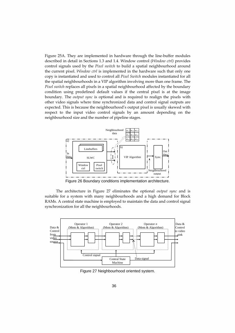
36
Figure 25A. They are implemented in hardware through the line-buffer modules described in detail in Sections 1.3 and 1.4. Window control (Window ctrl) provides control signals used by the Pixel switch to build a spatial neighbourhood around the current pixel. Window ctrl is implemented in the hardware such that only one copy is instantiated and used to control all Pixel Switch modules instantiated for all the spatial neighbourhoods in a VIP algorithm involving more than one frame. The Pixel switch replaces all pixels in a spatial neighbourhood affected by the boundary condition using predefined default values if the central pixel is at the image boundary. The output sync is optional and is required to realign the pixels with other video signals where time synchronized data and control signal outputs are expected. This is because the neighbourhood’s output pixel is usually skewed with respect to the input video control signals by an amount depending on the neighbourhood size and the number of pipeline stages.
Linebuffers
Window ctrl
Pixel switch
SLWC
...
VIP Algorithm
Sync.
a11 a12 a13
a21 a22 a23
a31 a32 a33
In data
Neighbourhood data
Neighbourhood output
Out data
a)
b)
Figure 26 Boundary conditions implementation architecture.
The architecture in Figure 27 eliminates the optional output sync and is
suitable for a system with many neighbourhoods and a high demand for Block RAMs. A central state machine is employed to maintain the data and control signal synchronization for all the neighbourhoods.
Central State
Machine
Operator 1 (Mem & Algorithm)
Operator 2 (Mem & Algorithm)
Operator n (Mem & Algorithm)
Data & Control to video
sink
Data & Control from video source
Control signal Data signal
Figure 27 Neighbourhood oriented system.

37
The memory synthesis tool developed in this thesis creates all the necessary memory and control functionality required for a functional spatio-temporal RTVPS. The required memory architecture specified within the IMEM for both spatial and temporal neighbourhoods is automatically optimized and mapped against the memory resources in such a manner that it produces an efficient implementation in terms of used resources. The tool also generates a VHDL template for the filter function, instantiates the filter and interfaces it with a memory management VHDL.
4.4 MEMORY IMPLEMENTATION
In a hardware implementation of RTVPS, only one operator can use the memory objects (Figure 8 and Figure 25) and all the memory objects are used simultaneously in the RTVPS. It is assumed that the memory objects can be grouped together to form global memory objects at the operator level. This grouping can be achieved through:
plinesiR wnW ×= (3)
where WRi is the width of the global memory object at the operator, nlines is the number of required line buffers for an operator and wp is the bit width representing a pixel. The length of the global memory object is equal to those of the memory objects that formed it, i.e. the image width [90]. This architecture is preferable to that of the direct mapping of memory objects to a memory location. This preference is because global memory objects require a minimal number of required memory entities in comparison to direct mapping architecture. Consequently, the number of memory accesses for an RTVPS operation is minimal for a global memory object.
To illustrate the formation of the global memory objects, consider an RTVPS operator that requires a neighbourhood of a 5x5 window with a 12-bit gray scale and a 640 by 480 frame size as the input video stream. This would result in the creation of four memory objects each of length L (=640) and width 12. The memory objects would be combined to create a GMO Ri of width 48. Figure 28 depicts this illustration where op_id represents the operator requiring the GMO.
L by 48
Ri
op_id = 1
L by 12
L by 12
L by 12
L by 12
Figure 28 Global Memory Object formation

38
4.5 MEMORY ALLOCATION
Single port memory configuration or a dual-port in which one port is used for writing and another for reading usually leads to unused memory areas because it allocates only one memory object to the Block RAM. If the memory object does not completely occupy the Block RAM there will be unused memory area. Figure 29 depicts an example of such an allocation. As shown, after the allocation of memory objects 1 and 2 to memory areas A1 and A2 on Block RAMs 1 and 2 respectively, the remaining memory areas B1 and B2 remain unused and subsequent memory objects will be allocated to other Block RAMs. Hence these types of memory allocation approaches can be very inefficient unless the allocated data is exactly the size of the memory module which is, however, very rarely the case.
Memory Object 1 A1
B1
Block RAM 1
Memory Object 2 A2
B2
Block RAM 2
Memory Object (width=12)
Memory Object (width=12)
a
b Allocation datapath width = 16 Figure 29. Traditional memory allocation.
Although, FPGA allows for the allocation of memory objects of any datapath
widths, it is however left to the designer to ensure the efficient use of the FPGA on-chip memories during memory allocation. Naturally, a higher datapath width is used when the width of the memory object is not a member of the datapath widths specified by the FPGA. Figure 29b shows an attempt to allocate an object of width 12 on Xilinx Spartan 3. Since a datapath width of 12 is not specified by the FPGA and 16 is the next datapath width that is a member of the Xilinx Spartan 3 datapath widths, allocation of the memory object is made using a datapath of 16. This will result in 4L bits being wasted, where L is the length of the memory object. An alternative is to partition the memory objects into using the supported widths.
These two sources of inefficient allocation are the reasons for researching both the allocation architecture and an algorithm based on the architecture that makes efficient use of memories. To achieve efficient allocation, the advantage of parallel accesses to Block RAMs through two independent ports is exploited.
4.5.1 Allocation algorithm
As presented by O’Nils et al. dual-port configuration of FPGA Block RAMs and global memory object allocation for RTVPS provide an efficient use of Block

39
RAMs [90]. An algorithm taking advantage of such efficient memory allocation techniques and the possibility of parallel accesses to Block RAMs through two independent ports will be presented in this section. Figure 30 shows attempts at finding an optimal use of the remaining memory resources identified in an FPGA Block RAM. If the remaining memory space is a single rectangular block as shown in Figure 30A, allocation is made to it through the second data port. If the remaining memory space is not a single rectangular block, it is divided into two rectangular blocks B and C as shown in Figure 30B. Allocation can be made to B or C through the second data port. Because Block RAMs currently support a maximum of two data ports, only block B or block C can be allocated depending on its size and the sizes of the memory objects awaiting allocation while the other block will never be used. As a result, the developed algorithm seeks the allocation for which the unused memory space is minimal by ensuring that, after allocation through port A, the remaining memory space forms a rectangular block, and by finding the memory object that uses as much of this block as possible. Hence, one of the indicators used in measuring the efficiency of the algorithm is the size of the unused memory resources.
Part of object 2
Useable memory
Memory Bank 2
Part of object 2
Memory Object 1
Memory Bank 1
Access via Data Port A
Access via Data Port B
Access via Data Port A
Access via Data Port B
A
Memory Object 1 A Unused
memory1
Block RAM 1
Unused memory C
Memory Object 1 A
Unused memory B
B
Unused memory C
Memory Object 1 A
Unused mem. B
Figure 30. Proposed memory allocation.
4.5.2 Definitions
To find the optimal use of the Block RAM, the algorithm must observe some definitions and constraints. These are listed as follows:
(i) M is the set of all the available Block RAM Mk and K is the number of Block
RAMs.

40
{ }KkMM k ,...,2,1== (4)
(ii) SMk is the size of the Block RAM Mk and is specified by the FPGA. For example, in Xilinx Spartan 2E FPGA SMk is 4096 bits [93]. The memory objects allocated to the Block RAM determine the length LMk and width WMk of Mk.
(iii) Wc is the set of all possible datapath widths Wn for Block RAMs on the FPGA. For example, 1, 2, 4, 8, and 16 are allowed on Xilinx Spartan 2E FPGA [93].
{ }NnWW nc ,...,2,1== (5)
(iv) R is the set of all memory objects Ri to be allocated and I is the number of memory objects.
{ }IiRR i ,...,2,1== (6)
(v) The size SRi of memory object Ri is defined as theproduct of the length LRi and the data width WRi of the memory object Ri.
RiRiRi WLS ×= (7)
(vi) Each global memory object is characterised by a quadruple of op_idRi, LRi, WRi
and xRi.
Ri(op_idRi, LRi, WRi, xRi ) (8)
where op_idRi is an identifier for the operator in which the memory objects making up the global memory object Ri are defined and xRi is the segment in which a memory object is located on the global memory object after partitioning into units of allowable data widths in Wc.
(vii) If WRi is not a member of Wc, Ri is partitioned into rj partitions such that the
width, wR, of each partition is a member of Wc where j = 1, 2, … J and J is the number of partitions in object Ri.
{ }JjWwxwLidoprR cRRiRiRiRiji i ,...,2,1,),,,_( =∈= (9)
(viii) Memory object Ri may be allocated to as many Block RAMs as required.
∑=
≤×K
kRiRiki SWL
1, (10)
where Li,k is the part of length LRi allocated at Mk. (ix) Block RAM only supports a maximum of two data ports. (x) Di,k is the decision to allocate some or all of the memory objects Ri at Mk. A
value of 0, 1 or 2 on Di,k means no allocation, single-port allocation or true dual-port allocation respectively.
∑=
2 ≤ I
ikiD
1, (11)

41
(xi) For all Ri in R and Mk in M that form part of the Di,k, the sum of the allocations may not be more than the size of the Block RAM.
∑=
≤×I
iiMkRiki SWL , (12)
(xii) For all Di,k, in the set of allocation decisions, AD, the unused memory space in Mk is defined as UMk.
∑=
×−=∈∀I
iiRikiMkkki WLSUMADD ,, , (13)
(xiii) The objective function of the algorithm is to minimize the sum of all UMk.
⎟⎟⎠
⎞⎜⎜⎝
⎛∈∀ ∑
kikki UMADD
,, min, (14)
To illustrate definitions (vi) and (vii), if the global memory object Ri of width 48 in Figure 28 were to be allocated on Xilinx Spartan 2E, Ri would then be partitioned into three rj each with a width of 16 since it is not possible to have a datapath width of 48 on a Spartan 2E. xRi will be 1, 2 and 3 for the first, second and third partitions indicating least, middle and most significant partitions on Ri. Figure 31 depicts this illustration.
L by 12
L by 12
L by 12
L by 12 L by 48
op_id = 1 xRi = 1
L by 16 op_id = 1 xRi = 3
L by 16 op_id = 1 xRi = 1
L by 16 op_id = 1 xRi = 2
Figure 31. Partitioning global memory object.
For every Block RAM available on the FPGA, attempts are made to allocate a
global memory object to it. The amount of unused memory space UMk is estimated. If UMk is zero, the allocation decision is stored and the iteration continues to the next memory object or Block RAM. Other possibilities are then considered such that UMk is minimal. The final decision is based on the allocations offering the least amount for the sum of the unused memory space on all Block RAMs. Figure 32 shows the allocation algorithm in relation to the definitions and constraints listed above before making the final decision. In the figure, any Ri is an allocation candidate to any Mk. Since Mk supports only two ports and in line with definition (x), only two Ris that minimize UMk can at most be selected such that our objective function, definition (xiii) is achieved after all Ris are allocated. According to definitions (vii) and (viii), a global memory object may be partitioned into many

42
smaller units and many Block RAMs. By exploiting FPGA parallel access to Block RAMs this enables the reconstruction of the object in order to achieve a throughput of one pixel per clock cycle.
M2
R2
Mk
Ri
MK
RI
M1
R1
…
…
…
…
K is number of available memory modules
I is number of memory objects to be allocated
Di, k
Mk is defined by LMk, WMk and SMk. SMk = LMk * WMk
Ri is defined by LRi, WRi and SRi. SRi = LRi * WRi
Figure 32. Allocation model.
4.5.3 Proposed algorithm
The proposed allocation algorithm is presented in Figure 33. A more detailed form of the algorithm in the form of pseudo-code is presented in Figure A.1 in Appendix A. In step 1, the algorithm creates global memory objects according to Eq. (3). In step 2, the algorithm ensures that the global memory objects conform to the allowable port width configuration according to definition vii. This step is captured in a procedure, configure_global_memory_objects(R), presented at the lower part of Figure A. Steps 3, 6, 7 and 8 ensure that the algorithm iterates through all the memory objects starting with the first. In step 4 the global memory objects are allocated to the Block RAMs according to definitions (viii) to (xi) while optimal use of unallocated memory space in the Block RAM through the second port is implemented in step 5, which is also in accordance with definitions (viii) to (xi). Optimal allocation is that for which the unused memory space is a minimum, preferably zero using either one or two ports in the Block RAM.
The Proposed Allocation Algorithm Algorithm: Memory Allocation(R, M) Parameters: R[R
1 … R
I] set of I memory objects;
M[M1 … M
K] set of K Block RAMs;
Return: MA[M
A1 … M
AK] set of K Allocated Block RAMs;
1. Create global memory objects (GMO) 2. Configure GMOs 3. Starting with the first GMO and the first Block RAM 4. Allocate GMO to Block RAM via port A. 5. If Block RAM is not fully used find maximum use of
remaining memory via port B using another GMO. 6. Select the next GMO when the current has been fully
allocated. 7. Select the next Block RAM when all the memory space
has been optimally used. 8. Return the set of allocated Block RAMs after
allocating all GMOs. Figure 33. The proposed allocation algorithm.
43
4.5.4 Complexity analysis
In estimating the complexity of the algorithm, the number of available Block RAMs, K, and the number of memory objects, I, after partitioning with respect to their width, play major roles. Since the algorithm conducts a single iteration through the sets of Block RAMs and two iterations through the set of memory objects as shown in steps 3, 4 and 5 in Figure 33 (see also Figure A in the Appendix), the allocation algorithm AA is a function of K and I and its complexity can be expressed as
( ) ( )2, IKIKAA ⋅Ο= (15)
The algorithm is thus, at worst, of the third order of the larger of K and I. Implementation costs depend on the representations of the properties of the Block RAMs, memory objects and allocation objects, and the arithmetic and logic operations defined for them.
4.6 ARCHITECTURE DRIVEN BLOCK RAM OPTIMISATION
To achieve architecture driven memory allocation targeting a given FPGA architecture, information about the amount and location of block RAMs, the structure and organization (number of rows and columns) of the logic elements and the amount of distributed RAM bits that can be implemented using the logic elements are read from the database. In addition, estimates concerning the number of logic elements, the block RAMs, the minimum clock frequency and other logic resources required to implement the video processing application are read from the high-level system specification. With this information, IMEM seeks an allocation alternative that uses the minimum number of block RAMs by allocating logical memory requirements below a threshold to CLBs. The threshold is determined by simulations for the given architecture and the clock frequency of the application. The threshold is chosen such that the power consumption by the CLBs implementing the logical memory does not exceed the power consumed by the block RAM. The objective of the proposed architecture driven allocation can be summarized as:
• Allocate logical memory requirement below a given threshold to
CLBs • Ensure power consumption by CLB allocation is not larger than
that by block RAM. The search for the lowest area and power costs is formulated as follows: MP is the set of memory partition defined within IMEM [91] in order to
allocate the line buffers in Figure 25 to physical memory.

44
MP = {mpi | i = 1, 2, …, I} (16)
The memory partitions in Eqn. 16 are created by a heuristics-based algorithm defined in Section 4.5 above, [91] (Figure 36, Figure 37) to efficiently allocate the GMOs, based on the memory architecture stated above in Eqn. 3. The algorithm creates the GMOs and partitions them to ensure that their widths are directly supported by the FPGA block RAMs. It also takes advantage of the dual port capabilities of the Block RAMs, with independent read and write accesses at both ports, to achieve near optimal allocations and the possibility of allocating a GMO to as many Block RAMs as is required. The allocation algorithm in Section 4.5 will be augmented by a Block RAM usage minimization goal described in this section. The intermediate result consisting of memory partition ready for allocation is the memory requirements input to this minimisation work.
CLBS defines the set of CLBs available in the FPGA organized in terms of rows r and columns c.
CLBS = {clbr,c | r = 0, 1, …, R -1 ^ c = 0, 1, …, C -1} (17)
where R and C represent the number of CLB rows and columns in the FPGA respectively. CLBS’ (= R · C) gives the number of CLBs in the FPGA. BRAMS defines the number of FPGA block RAMs and their location given in terms of row rr and column cc.
BRAMS = {bramrr,cc | rr = 0, 1,…, RR -1 ^ cc = 0, 1,…, CC -1} (18)
where RR and CC represent the number of block RAM rows and columns in the FPGA respectively. BRAMS’ (= RR · CC) gives the number of BRAMs in the FPGA. The total logic area required (TLR) in terms of CLBs to implement the tasks in the video processing is calculated as
∑=
=K
kktlrTLR
1
(19)
where tlrk is the number of CLBs required by task k and K is number of tasks in the dataflow graph (Figure 24). Eqn. 19 can be estimated from the datasheet of the IP cores or from a database of the filters previously implemented for the RTVPS and currently being re-used. After estimating the task area cost, the tool must estimate the amount of CLB resources available for memory allocation by through using Eqn. 20.
)( MFTLRCLBSACLB +−= (20)
where MF in Eqn. 20 is the Mark-up Factor used to denote the amount of logic in terms of CLBs required to link different tasks together and to the modules implementing their memory sub-system as shown in Figure 26. MF can be given as an estimate or be determined from the datasheet for each task. The expressions for the allocation cost of a given logical memory requirement to distributed RAMs or Block RAMs are defined as:
45
∑=
×⋅×−
=J
jCLBCLB RjP
JACLBACCLB
1
)(1_ (21)
BRAMBRAMBRAM
RPA
ACBRAM ××−×
=12
1_ (22)
Eqn. 21 provides an expression for estimating the cost (CLB_AC) of allocating a given memory partition to CLBs J. It is defined as functions of the available CLBs, required CLBs, power consumption PCLB by the CLBs and associated routing resources [45], [40] across the CLBs. Eqn. 22 gives the cost (BRAM_AC) of allocating the same amount of memory to a single port of a dual ported BRAM. Hence allocation utilizes only one of the two ports times the number of available BRAMs. The cost is also given in terms of the power consumption of the BRAM PBRAM and signal routing RBRAM. The Power consumption resulting from interconnect routing is not considered due to the estimation complexity already in pre-place-and-route high-level design environment. There will be a reduction in the power consumption resulting from moving data the allocation from block RAMs to the distributed RAM. This is because data will be allocated locally where they are required and hence avoiding routing to a specific block RAM site. However RCLB and RBRAM are routing factors for CLB and block RAMs to account for the interconnection and can be determined by mean of simulation.
Figure 34 shows the architecture driven memory allocation optimization approach. It requires the memory partitions from within the IMEM environment and information about CLBs and BRAMs read from the architecture description file (ADF). ADF contains information concerning the essential features of the target FPGA. In addition, estimates of the amount of CLB required to implement the tasks (Figure 24, Figure 25) in the design are read from the IP core datasheets.
Step 1 in Figure 34 determines the maximum amount ML of bit that can be allocated using CLB distributed RAMs based on the application frequency and the power consumption data for distributed and block RAMs of the target FPGA. Using ML the set of memory partitions MP to be allocated will be divided into those that can only be allocated using BRAM and those that might be allocated to the distributed RAM or block RAM.
The choice of allocation of smaller memory partitions that are candidate for either distributed or block RAM memory is motivated by Eqn. 8 and Eqn. 9. Step 5 performs dual port memory allocation of memory partition mpi larger than ML based on the algorithm in Section 4.5. Steps 6 to 13 compare the estimated power consumption and allocation cost of the CLBs and BRAM required to allocate costs fof a given memory partition mpi. The option that offers the lower cost is chosen. Step 2 ensures that preference is given to larger memory partitions during block RAM allocation whereas step 6 ensures the reverse during distributed RAM allocation. The approach in Figure 34 has been implemented and incorporated into the IMEM toolset to improve its memory management efficiency.

46
Architecture drive memory allocation Algorithm: Power Optimization(ADF, IMEM) 1: ML = memory_upper_limit(freq, ADF) /* Allocate large memory objects to BRAMs */ 2: sort(mp, ‘descending’) 3: for each mpi in MP 4: if sizeof(mpi) > ML 5: perform_dual_port_allocation(mpi,IMEM) /* Allocate small memory objects using cost */ 6: sort(mp, ‘ascending’) 7: for each mpi in MP 8: if sizeof(mpi) < ML { 9: estimate no of CLB required to allocate mpi /* Using Eqn. 8 */ 10: estimate CLB allocation cost for mpi /* Using Eqn. 9 */ 11: estimate BRAM allocation cost for mpi /* Choose allocation option with lower cost */ 12: select CLB/BRAM allocation with lower cost 13: update allocation_cost }
Figure 34 Architecture driven memory allocation
4.7 MEMORY ACCESSING
The allocation software ensures that each entry of a Block RAM data object stores information concerning the width and length of the GMO segment allocated to it, the port used for allocation and the hierarchy of its segment in the GMO. In addition, each partition stores information about the Block RAM to which it is allocated, the port of allocation and its start address on the Block RAM, the GMO and segment to which it belongs.
The advantage of sequential accesses to memory for RTVPS applications can lead to improved memory performance by using pointers whose values increase whenever there are valid pixel values. Using the GMO architecture further reduces the number of such pointers to one for each RTVPS operator. The pointers may be implemented by using a single counter for each GMO, further referred to as the base pointer, or by using a counter for each partition in a GMO, further referred to as the distributed pointers.
To this end, the results from the memory allocation stage are imported into the address generation module. From these allocation results GMOs are reconstructed, and address spans for each partition in a Block RAM are generated. The start and end addresses for each partition are calculated. Offsets are

47
considered where dual ports are used for the allocation on Block RAMs for different partitions in order to avoid memory overlap. The generated addresses are used to determine the location of each GMO element. Two approaches for accessing the GMO elements have been developed, namely the base pointer approach and the distributed pointer approach and these are presented as follows. These two approaches are depicted in Figure 35 while details of their implementations are presented in the following subsections.
GMO 1
Length = L L = p1 + p2
Partition 1 Length = p1
Partition 2 Length = p2
Base Pointer base = 0 – L - 1
0 p1 - 1 0 p2 - 1
BR1 BR2
if base < p1 access BR1 else access BR2
offset
(a)
(b)
GMO 1 Length = L L = p1 + p2
Partition 1 Length = p1
Partition 2 Length = p2
0 p1 - 1 0 p2 - 1
BR1 BR2
offset
Figure 35 Two memory accessing approaches
4.7.1 Base Pointer Approach
In this approach, a single pointer is used to track the location of the element to be accessed in the GMO. The pointer starts at zero and increases to one less than the length of the GMO and then resets to zero. Since the memory accesses are clocked, the value of the pointer increases with clocked access to the Block RAM when there are valid data. Address spans for each partition of the GMO are used to determine the relevant Block RAM relating to the element accessed, depending on the value of the pointer. Hence, only the relevant Block RAMs are enabled while the other related Block RAMs are disabled. Figure 35a, depicts this approach for a simplified case in which a GMO consists of a single segment with two partitions.
In the figure, partitions p1 and p2 are allocated to Block RAMs BR1 and BR2. From Figure 35a, when the value of the counter base is within the span of p1, the appropriate port on BR1 is enabled and accessed while the relevant port on BR2 is disabled. The reverse is the case when base is no longer within the span of p1, i.e. within the span of p2. This simple example could be extended to cases in which

48
more than one segment makes up a GMO and each segment has more than 2 partitions. A formal description of this approach is shown in Figure 36a.
Figure 36b depicts the base pointer implementation of the GMO shown in Figure 31. In the figure, BR1_EN_A, BR2_EN_A and BR2_EN_B represent the enable signals on port A of BR1, port A of BR2, and port B of BR2 respectively. Likewise, BR1_A_Adr, BR2_A_Adr and BR2_B_Adr are the address signals on port A of BR1, port A of BR2, and port B of BR2 respectively. A Block RAM is enabled or disabled by assigning ‘1’ or ‘0’ to its enable signal.
(a)
For each GMO: • create Address Table from segments and partitions that make up the
GMO to determine when to enable Block RAMs among related partitions
• create an incrementable pointer of length ( )⎡ ⎤L2log which increases when there are valid pixel values
• using Address Table and pointer value enable appropriate Block RAMs and set the values of address signals.
(b)
512 by 32
op = 1 seg = 1 par = 1
BR1 Port A
128 by 32
op = 1 seg = 1 par = 2
640 by 16 op = 1 seg = 2 par = 1
BR2 Port B Port A
offset=320
0 ≤ bp ≤ 639 BR2_EN_A = 1 BR2_A_Adr = bp
512 ≤ bp ≤ 639 BR2_EN_B = 1 BR2_EN_B = 0 BR2_B_Adr = offset + bp - 512
0 ≤ bp ≤ 511 BR1_EN_A = 1 BR2_EN_B = 0 BR1_A_Adr = bp
Base Pointer bp = 0 - 639
Figure 36. Base Pointer Approach.
4.7.2 Distributed Pointer Approach In this approach, each partition is handled separately, starting with the first
partition in a segment. Local pointers equal in length to that of each partition are created. As long as the enable signal of Block RAM for a partition is high, memory access is initiated at its first position using its pointer and continues incrementally, if valid data are available until its full length is achieved. During this period, the partition ensures its enable signal is re-asserted while the enable signals of the neighbouring partitions of the same segment are de-asserted. Controls are transferred to the next partition of a similar segment when the upper limit of the partition is reached. If however, the partition is the last in the segment, controls are transferred to the first partition. Since the address buses of partitions on Block RAMs provide appropriate bit vectors to cover their entire lengths, they are used

49
as the local pointer. In this approach, the enable signals of all the first partitions are set to high at start-up to ensure that memory accesses start with the first partitions. Figure 35b depicts this approach. A simplified case of a GMO consisting of a single segment with two partitions p1 and p2 allocated on Block RAMs BR1 and BR2 respectively is considered in Figure 35b. Figure 37a and Figure 37b show formal descriptions and implementations of the GMO depicted in Figure 31 using this approach respectively. Signals in Figure 37b have similar meanings to those in Figure 36b. Since the 640-by-16 partition is the only one in its segment, it is always enabled and the address is reset to 0 when it reaches its upper limit.
For each segment in each GMO: • create Address Table for each partition in the segment • create an incrementable pointer of length ( )⎡ ⎤p2log which increases
when there are valid pixel data for partitions in the segment • start memory access with the first partition with start address of 0 • enable Block RAM of currently active partition and disable Block
RAMs of related partitions while pointer is less than partition’s length • if pointer of active equals partition’s length less one, reset it to 0,
disable it and enable next (or first partition if this is the last partition).
(a)
(b) 512 by 32
op = 1 seg = 1 par = 1
BR1 Port A
128 by 32
op = 1 seg = 1 par = 2
640 by 16op = 1 seg = 2 par = 1
BR2 Port B Port A
offset=320
BR2_EN_A = 1 & BR2_A_Adr< 639
BR2_A_Adr = BR2_A_Adr + 1
BR2_EN_A = 1 & BR2_A_Adr= 639
BR2_A_Adr = 0 BR2_EN_A = 1
BR2_EN_B = 1 & BR2_B_Adr < offset + 127 BR2_EN_B = 1 BR2_EN_B = 0 BR2_B_Adr = BR2_B_Adr + 1 BR2_EN_B = 1 & BR2_B_Adr = offset + 127 BR2_EN_B = 0 BR2_EN_B = 1 BR2_B_Adr = offset
BR1_EN_A = 1 & BR1_A_Adr < 511 BR1_EN_A = 1 BR2_EN_B = 0 BR1_A_Adr = BR1_A_Adr + 1 BR1_EN_A = 1 & BR1_A_Adr = 511 BR1_EN_A = 0 BR2_EN_B = 1 BR1_A_Adr = 0
Figure 37. Distributed Approach.
4.8 CONSTRAINT GENERATION
To generate constraints targeting a given FPGA architecture, the information about the amount and location of block RAMs, the clock regions, the number of logic elements within each clock region and used IO pins, is read from the database. In addition, the amount of logic elements, block RAMs and other
50
resources required to implement the design is read from the synthesis report. With these two sets of information, block RAMs are placed in clock regions closest to most of the IO pins and design logics are constrained to be placed as close to the used block RAMs as possible. The approach is shown in Figure 38. Placement of both the design logic and block RAMs is such that a minimal number of clock regions is used. This approach is suitable for video processing systems because they are data dominated thus requiring large memory accesses to block RAMs. Constraining logic to be placed close to block RAMs within a minimal number of clock regions leads to reduced interconnections, shorter delays and reduced power consumption. However, the number of block RAMs may require more than one block RAM column, thus requiring placement across the FPGA chip. For this scenario, logic elements are placed such that they are equidistant from the two block RAM columns. Placement is further optimized by using a logic element based placement constraint in addition to the clock regions.
The place and route constraints are generated for the memory subsystem of each task in the system dataflow graph (Figure 24) whereas the filters are made to overlap many memory subsystems. For this work we have used the Xilinx Spartan 3 FPGA. However, the approach can be adapted for any FPGA architecture. The automatically generated constraints will now be presented.
OPTIMIZATION GOAL [94]: The synthesis reports show that
the designs can meet the frequency requirements hence placement can be optimized for area by setting the constraint OPTIMIZE to AREA. Other possible values are SPEED and BALANCE.
OPTIMIZATION EFFORT [94]: The overall, placement and
router optimization efforts are set to high through the constraint OPT_EFFORT = HIGH. This may require more implementation time but the results are always better. Alternative values are NONE, STANDARD and MEDIUM.
DESIGN HIERARCHY [94]: Design hierarchy is dissolve by
setting the constraint KEEP_HIERARCHY to FALSE in order to flatten the design. This choice increases the possibility of logic sharing and optimization. The alternative value is TRUE.
RELATIVE LOCATION [94]: the design is constrained to use
relative location in order to relationally place logics and block RAMs based on their functions and hierarchy by setting the constraint USE_RLOC to TRUE. In this way block RAMs whose inputs or outputs connect to IO pins are placed as close to the IO pins as possible while other block RAMs are placed relative to them. The alternative value is FALSE.

51
DESIGN GROUPS [94]: the entire design can be grouped according to the system flow graph (Figure 24) into small components to manage the design complexity. The memory sub-component of each task in Figure 24 is defined as an area group and placed by clock regions. The filters in all the tasks are grouped together into an area group and placed in such a way that it overlaps other area groups. This is to allow for flexible inter-group communication. Compact placement of the area groups is ensured by setting the COMPRESSION factor of each group to the highest (100%). Figure 38 shows in pseudo-code the constraint generation approach
presented in here. The resource requirement of all the line-buffers are read from the IMEM model and are collected in a set LB whereas the resources available in each of the clock-regions are read from the database and collected in a set CR. Each LBi and CRj,k is defined in terms of the amount of block RAMs, multipliers, and logic blocks. The algorithm searches for a set of CRj,k that satisfies all the resource requirements for all the LBis and for which the over-all difference in area requirements and occupied area is minimal. LBAi and CRAj,k are the area requirements up to LBi and the available resources up to CRj,k respectively. Figure 39 depicts the clock distribution of a design case (discussed in the next section) implemented without (A) and with (B) the constraints. From Figure 39 it is obvious that the implementation without constraints will consume more dynamic power since it occupies a larger area and requires a wider clock network. Figure 40 shows the workflow by which the IMEM tool set automatically generates the place and route constraints. All the required information is gathered from the IMEM model of the system flow graph (Figure 24, Figure 26) and FPGA architecture. The output of the algorithm is a user constraint file (UCF).

52
/* Gather background information */ CR = read_clock_region_info() LB = read_linebuffers_resource_use(IMEM) /* expression for estimating area cost*/
∑=
=i
xxi LBareaLBA
1
)(
∑==
=kj
zyzykj CRareaCRA
,
1,1,, )(
ikj LBACRAtarea −= ,cos_
/* Using area as cost criterion, find the CRj,ks to in which to place LBis with minimal cost */ generate_placement_constraint(LBi,CRj,k){ write placement constraint for LB1 at CR1,1 for each LBi {/* i > 1 */ for each unused_cr { estimate area_cost select CRj,k with minimum area_cost write PAR constraint for LBi at CRj,k update area_cost } } }
Figure 38. Constraint generation algorithm
A) B)
Figure 39. Clock distributions showing the effect of constraints

53
IMEM Model
Task RTL
Placement constraints
Memory RTL RTL Synthesis
Place & Route FPGA
FPGA Architecture
database
User generated
IMEM generated
Third Part Tool
RTVPS Specifications
Figure 40. Constraint generation workflow
4.9 RESULTS
In this section the results obtained after implementing the algorithm and the analysis of its performance are presented as follows. Section 4.9.1 presents the performance of the algorithm under real-time video processing design. Section 4.9.3 presents its performance, under two test scenarios modelled upon one of the real-time design cases. The performance of the memory synthesis with varying memory requirements and Block RAM sizes is presented in Section 4.9.4. Section 4.9.5 presents the performance analysis for eleven video processing systems published by other researchers. Section 4.9.7 compares the performance of the two memory addressing schemes presented in Section 4.7.
4.9.1 Real-time video processing design cases
The algorithm has been implemented in C++ using the object-oriented approach. The implementation was simulated using the memory requirements of real-time video processing design cases [90]. The first design case was a spatio-temporal median filter with a neighbourhood of seven frames and two line buffers. Two instances of this design case were considered. The first, (1-1), being a VGA frame with 24-bit RGB pixels and a 640 frame length while the second, (1-2), was a PAL frame with an 8-bit gray scale pixel and a 708 frame length. The second design case was a machine vision system with a median filter, segmentation and three 1-bit morphological operations. For this design case two instances were also considered. The first case, (2-1), being an 8-bit gray-scale, which had a VGA resolution as its input video stream, while the second, (2-2), had a 12-bit gray scale with a 1.3 MPixel resolution as its input video stream. Table 2 shows the summary of the memory requirements for the design cases considered. In the table column 2 shows the number of video processing filters in the design case while column 3 shows the number of line buffers required by each filter. For design cases 1-1 and 1-2 seven 3x3 filters were used, each requiring two line buffers while for design cases 2-1 and 2-2, one 5x5 median filter, one segmentation operation and three 17-
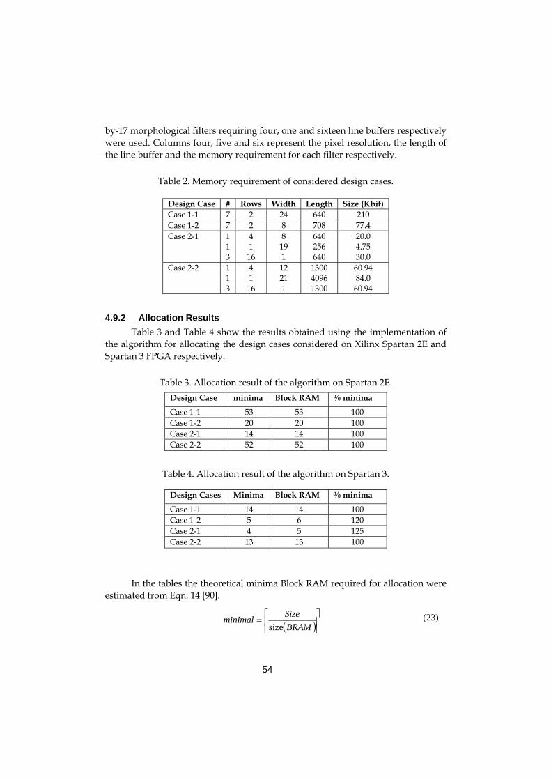
54
by-17 morphological filters requiring four, one and sixteen line buffers respectively were used. Columns four, five and six represent the pixel resolution, the length of the line buffer and the memory requirement for each filter respectively.
Table 2. Memory requirement of considered design cases.
4.9.2 Allocation Results
Table 3 and Table 4 show the results obtained using the implementation of the algorithm for allocating the design cases considered on Xilinx Spartan 2E and Spartan 3 FPGA respectively.
Table 3. Allocation result of the algorithm on Spartan 2E.
Table 4. Allocation result of the algorithm on Spartan 3.
In the tables the theoretical minima Block RAM required for allocation were
estimated from Eqn. 14 [90].
( )⎥⎥
⎤⎢⎢
⎡=
BRAMSizeminimal
size (23)
Design Case # Rows Width Length Size (Kbit) Case 1-1 7 2 24 640 210 Case 1-2 7 2 8 708 77.4 Case 2-1 1
1 3
4 1
16
8 19 1
640 256 640
20.0 4.75 30.0
Case 2-2 1 1 3
4 1
16
12 21 1
1300 4096 1300
60.94 84.0 60.94
Design Case minima Block RAM % minima
Case 1-1 53 53 100 Case 1-2 20 20 100 Case 2-1 14 14 100 Case 2-2 52 52 100
Design Cases Minima Block RAM % minima
Case 1-1 14 14 100 Case 1-2 5 6 120 Case 2-1 4 5 125 Case 2-2 13 13 100

55
where Size is the number of bits required by the design case, given in column 6 of Table 2, and the size of BRAM is the numbers of bits in one block RAM, 4 Kbit for a Xilinx Spartan 2E and 16kbit (without parity) for Spartan 3 [93], [50]. Table 3 shows that the algorithm requires no more than the minimum value for the allocation of each of the design cases on Spartan 2E. Hence, it is in total agreement with the minimum requirements for Spartan 2E. On Spartan 3, allocation requirements were equal to the minimum values except for two of the design cases. The minimum value is calculated for the allocation on a Block RAM with an infinite number of ports. The minimum value, however, only indicates the effectiveness of the allocation but not its feasibility, since it is not possible to have Block RAMs with an infinite number of ports. The implementation for Spartan 3 did not consider parity. The parity feature on Xilinx Spartan 3 FPGA increases the available Block RAM size by providing an additional bit for every 8 bits [50]. When the parity bit is taken into consideration it makes it possible to have width configurations that are multiples of the 9-bit on the Block RAM. In this manner, 18Kbits of Block RAM size can be achieved instead of 16Kbits. This parity feature was not considered since it is only specific to some of the Xilinx FPGA families and not all FPGAs have this feature. From Table 4, the non-minimum result of the algorithm in design cases 1-2 and 2-1 is because, if a design case has many operators in relation to the total storage requirement and/or the size of each Block RAM, the number of ports on each Block RAM will limit the allocation.
Figure 41 shows the mapping of the memory objects to the Block RAMs for the design Case 2-1 on Xilinx Spartan 2E. The identifiers of the global memory objects and the Blocks RAMs are shown. In addition, the figure shows that memory objects were allocated to as many Block RAMs as required. This is a case of dynamic partitioning with respect to the length. In the figure, each block is annotated by “WxL” and “op_id: y” where W, L and y represent the width, memory depth and operator id of the allocated partition respectively. BRAMs 7 and 8 in the figure exploit the independence of the data path width and memory depth for the two ports on a dual-ported RAM. In BRAM 7, Port A is allocated with a partition which has a data path width of 2 and a depth of 256 while Port B is allocated with a partition with a data path width of 16 and a depth of 224.
In Figure 41 memory object 1 of width 32 bits and length 640 was firstly partitioned width-wise into two partitions each of width 16 bits and length 640. Then the first partition was allocated to Block RAMs 1, 2 and 3, by partitioning it length-wise and allocating partitions of lengths 256, 256 and 128 respectively, completely filling the Block RAMs 1 and 2 using only one port. The second partition of memory object 1 was also partitioned length-wise and allocated to Block RAMs 3, 4 and 5. This width-wise and length-wise partitioning of the memory object makes it possible to allocate a memory object to many Block RAMs and to configure the memory object with widths feasible in the FPGA. In the figure, the lower and upper allocations were through ports A and B respectively. The figure also indicates the width and length of the memory objects allocated at

56
each Block RAM. In addition, unused memory space is specified on Block RAM 14 where it occurred. This memory space can be used through the second port.
Figure 41. Memory allocation of Case 2-1 on Xilinx Spartan 2E FPGA.
4.9.3 Performance analysis with varying length and width To test the performance of the algorithm, the memory requirements for
allocation were varied under two scenarios such that they are similar to design case 1-1. The two test scenarios are presented as follows.
4.9.3.1 First test scenario
In this test scenario, four frame lengths L (320, 640, 1280 and 2560) were used while the widths W were determined by the memory requirement, which was allowed to vary from 100kbit to 2000kbit. This test scenario was simulated for XILINX Spartan 2E and 3 FPGA. The minimum Block RAM allocation was plotted along with the estimated Block RAMs for the four values L. On Spartan 2E, the minima were equal to those estimated by the algorithm for all values of L whereas on Spartan 3, the minima differed from the values obtained for L = 320 and the estimated values obtained for other values of L equalled the minima for most of the memory requirements. Figure 42 shows the performance of the algorithm for this test scenario.

57
Figure 42a. First test scenario on Spartan 2E.
Figure 42b. First test scenario on Spartan 3.
4.9.3.2 Second test scenario
In this test scenario, four values of width W (3, 6, 12 and 24) were used while the length L was determined by the memory requirement, which also ranged from 100 to 2000 Kbits. The test scenario was simulated for Spartan 2E and 3. The results obtained for the theoretical minima and the estimated Block RAMs for the different values of W were equal when Spartan 2E was used but differed when memory

58
requirements less than 200kbit on Spartan 3 were used. Figure 43 shows the performance of the algorithm for this test scenario.
As shown in Figure 42 and Figure 43, allocations on Spartan 2E equalled the theoretical minima whereas those on Spartan 3 differed slightly. This is because the Block RAM sizes are smaller in Spartan 2E and were more easily managed. In Figure 42b, allocations with L=320 required I excess of the theoretical minima due to the small sizes of the memory objects with respect to the sizes of the Block RAMs. The average variation of the number of Block RAMs from the theoretical minima is 6%. In Figure 43b, the first allocation using W=3 had a variation of 14% from the theoretical minima also due to the small sizes of the memory objects. Configuring the global memory objects width-wise to only data-path widths allowed by the FPGA technology leads to the efficient utilization of the Block RAMs. This enables the allocation results to be close to the theoretical minima.
By definition, the theoretical minimum assumes a Block RAM with an infinite number of ports making it possible to allocate to the Block RAM until it is fully used. It is not a practical value but rather a metric used to measure the optimality of the algorithm. Consequently, the higher the number of ports on Block RAMs the closer the algorithm result is to the theoretical minimum.
Figure 43a. Second test scenario on Spartan 2E.
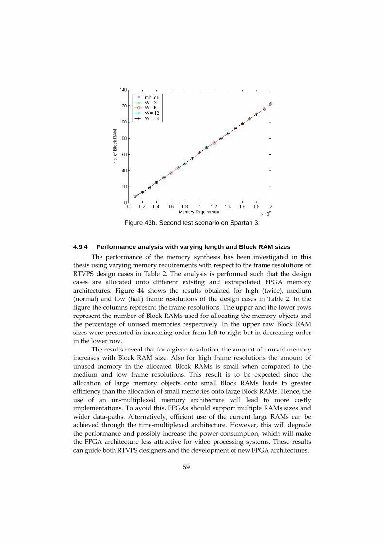
59
Figure 43b. Second test scenario on Spartan 3.
4.9.4 Performance analysis with varying length and Block RAM sizes The performance of the memory synthesis has been investigated in this
thesis using varying memory requirements with respect to the frame resolutions of RTVPS design cases in Table 2. The analysis is performed such that the design cases are allocated onto different existing and extrapolated FPGA memory architectures. Figure 44 shows the results obtained for high (twice), medium (normal) and low (half) frame resolutions of the design cases in Table 2. In the figure the columns represent the frame resolutions. The upper and the lower rows represent the number of Block RAMs used for allocating the memory objects and the percentage of unused memories respectively. In the upper row Block RAM sizes were presented in increasing order from left to right but in decreasing order in the lower row.
The results reveal that for a given resolution, the amount of unused memory increases with Block RAM size. Also for high frame resolutions the amount of unused memory in the allocated Block RAMs is small when compared to the medium and low frame resolutions. This result is to be expected since the allocation of large memory objects onto small Block RAMs leads to greater efficiency than the allocation of small memories onto large Block RAMs. Hence, the use of an un-multiplexed memory architecture will lead to more costly implementations. To avoid this, FPGAs should support multiple RAMs sizes and wider data-paths. Alternatively, efficient use of the current large RAMs can be achieved through the time-multiplexed architecture. However, this will degrade the performance and possibly increase the power consumption, which will make the FPGA architecture less attractive for video processing systems. These results can guide both RTVPS designers and the development of new FPGA architectures.

60
416
3264
128256
0
10
20
30
40
Design Cases
Low Resolution
RAM size
# of
RA
M u
sed
1 11 2
2 12 2
416
3264
128256
0
20
40
60
Design Cases
Medium Resolution
RAM size
# of
RA
M u
sed
1 11 2
2 12 2
416
3264
128256
0
50
100
150
Design Case
High Resolution
RAM size
# of
RA
M u
sed
1 11 2
2 12 2
256128
6432
164
0
20
40
60
80
100
Design CasesRAM size
% o
f RA
M u
nuse
d
1 11 2
2 12 2
256128
6432
164
0
20
40
60
80
100
Design CasesRAM size
% o
f RA
M u
nuse
d
1 11 2
2 12 2
256128
6432
164
0
20
40
60
80
100
Design CaseRAM size
% o
f RA
M u
nuse
d
Figure 44. Block RAM usage with varying memory requirements
4.9.5 Performance Analysis for video processing systems
In this section, the performance test of the allocation algorithm on video processing systems published in the literature [78]-[87] is presented. The tests are still in manuscript form and are to be sent for publication after further extensive testing. The algorithm was implemented using Block RAM sizes of 2, 4, 8, 16 and 32Kbits, each with data path width configurations of 2, 4, 8, 16, 32 bits.
The average results for the allocation of the test designs [78]-[87] are shown in Table 5 The results for all design cases were combined together in order to observe the memory sets producing the best allocation results. The most satisfactory allocation results were acquired using a RAM size of 8Kbits and a data path width of 16 or 32 bits, and this achieved an average allocation efficiency of 92.5%. However, larger memory sets, up to 16Kbit, also generated satisfactory results when combined with wide data path widths.
The use of large memory sets, as predicted, proved to be inferior to that for small sets in the majority of cases which is in agreement with the allocation results for the architecture initially produced by O’Nils in [90]. The allocation efficiencies of the algorithm on RAMs with a size corresponding to the configuration of a Xilinx Spartan-2 and Spartan-3 are presented in Table 6 and Table 7. On both Spartan-2 and Spartan-3, the algorithm achieves a 100% allocation efficiency in 9 out of 11 cases.
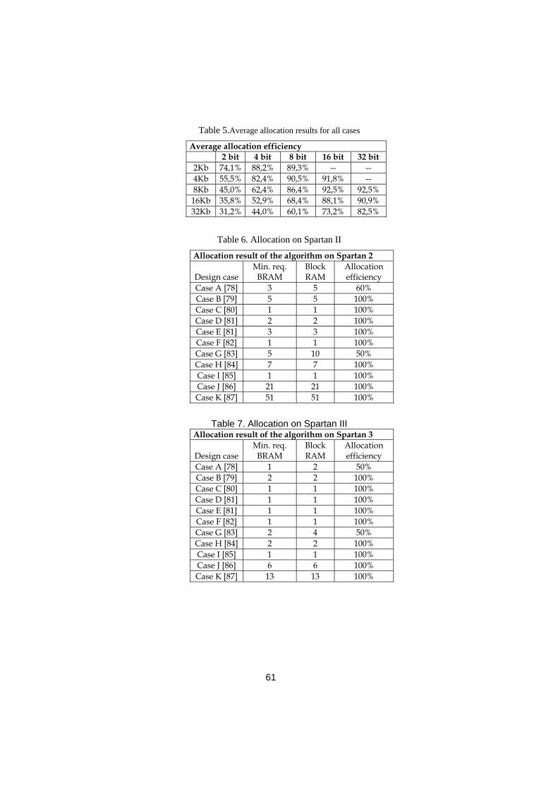
61
Table 5.Average allocation results for all cases
Average allocation efficiency 2 bit 4 bit 8 bit 16 bit 32 bit
2Kb 74,1% 88,2% 89,3% -- -- 4Kb 55,5% 82,4% 90,5% 91,8% -- 8Kb 45,0% 62,4% 86,4% 92,5% 92,5%
16Kb 35,8% 52,9% 68,4% 88,1% 90,9% 32Kb 31,2% 44,0% 60,1% 73,2% 82,5%
Table 6. Allocation on Spartan II
Allocation result of the algorithm on Spartan 2
Design caseMin. req. BRAM
Block RAM
Allocation efficiency
Case A [78] 3 5 60% Case B [79] 5 5 100% Case C [80] 1 1 100% Case D [81] 2 2 100% Case E [81] 3 3 100% Case F [82] 1 1 100% Case G [83] 5 10 50% Case H [84] 7 7 100% Case I [85] 1 1 100% Case J [86] 21 21 100% Case K [87] 51 51 100%
Table 7. Allocation on Spartan III
Allocation result of the algorithm on Spartan 3
Design caseMin. req. BRAM
Block RAM
Allocation efficiency
Case A [78] 1 2 50% Case B [79] 2 2 100% Case C [80] 1 1 100% Case D [81] 1 1 100% Case E [81] 1 1 100% Case F [82] 1 1 100% Case G [83] 2 4 50% Case H [84] 2 2 100% Case I [85] 1 1 100% Case J [86] 6 6 100% Case K [87] 13 13 100%

62
4.9.6 Performance of Architecture Driven Memory Allocation To test the effect of considering the FPGA architecture in memory allocation
as presented in Section 4.6, Design cases 1-1 and 2-1 in Section 4.9.1 were used. Although the two design cases were specified for 8-bits VGA resolution video streams, for the purpose of these tests the pixels were allowed to have values of 6, 8 9 and 10 bits whereas the frame width were given the values 256, 320 512, 640 and 800. The stretching of the pixel and frame resolutions was carried out to observe how the synthesis tool will perform under various memory requirements. Figure 45 shows the block RAM memory usage for the design cases under various pixel and frame resolutions. In the figure, columns such as ‘6w’ report block RAM usage by the allocation in Section 4.5 which finds an efficient method of memory allocation but without considering the possibility of allocation to distributed RAMs as presented in this thesis.
The designs were implemented according to the architecture in Figure 26 which abstracted the memory subsystem from the task. Hence configuring the memory requirements does affect the tasks configuration, the exception being through generic parameters. The designs were synthesized and analyzed for post-place and route simulation for power consumption. We found minimal changes in the number of CLBs used (between 6 and 12) and small changes in the power consumption. We have not presented the changes in either the CLBs or the power consumption because they were rather small and constant. Figure 46 shows the post-place and route clock distribution of the design case 2 using the approaches adopted in Section 4.5 and Section 4.6. The figure shows that logic distribution is concentrated on the right-side of the chip where most of the instantiated block RAMs are located as well as the centre where the clock network is most efficient.
66w
8
8w
99w
10
10w
800 512
256
0
2
4
6
8
Bits / Pixel
Design Case 1
Frame Width
# of
RA
M u
sed
w - without optimisation

63
66w
8
8w
99w
10
10w
800 512
256
0
2
4
6
8
Bits / Pixel
Design case 2
Frame Width
# of
RA
M u
sed
w - without optimisation
Figure 45. Memory usage
A) B)
Figure 46. Post-PAR Clock distribution of design case 2
4.9.7 Results of the addressing Table 8 shows the resources required to access the allocated memory objects
for the design cases in Table 2, the number of Block RAMs required for the allocations and the hardware operating frequency for the two approaches. Xilinx Spartan 3 FPGA was the target platform for implementing both approaches.
Table 8. Comparison of the two approaches.
Case 1-1 Case 1-2 Case 2-1 Case 2-2 BP Dist BP Dist BP Dist BP Dist No. of 4 input LUTs: 653 994 334 356 155 191 560 804 No. of BRAMs: 14 14 6 6 5 5 13 13 Max. Frequency (MHz): 116 186 106 183 140 214 91 173 Frequency Comparison (%): 100 160 100 173 100 153 100 190

64
Depending on the number of partitions relating to a GMO, address look-up
tables are required to set the enable signals and the values of the address signals to the appropriate Block RAMs on which the element of the GMO currently being pointed at is allocated, while also disabling related Block RAMs. In the Base Pointer Approach, these accesses to the Block RAMs are centrally controlled at the GMO level using a pointer. Hence, only one set of address look-up tables is required for each GMO. By contrast, in the Distributed Approach, each partition has its separate address look-up table, unrelated to those of related partitions. The use of a partition’s address look-up table depends on the value of its enable signal. Hence the total number of address look-up tables for one GMO depends on the number of partitions making up the GMO. This is evident by comparing Figure 36c and Figure 37c. The first row of Table 8 confirms this. Thus the Base Pointer Approach yields more efficient use of hardware resources than does the Distributed Approach. The differences in resource requirements are however marginal, amounting to less than 3% of the available resources, for example, Xilinx Spartan 3 XC3S400 series [48].
Delays associated with large counter values in single based pointers and the distribution of the pointer values are eliminated in the Distributed Pointer Approach since each Block RAM partition has one local pointer. The use of small counters to evaluate addresses for each partition in the Distributed Pointer Approach increases the speed of memory accesses and consequently, increases operating frequency. This is because all signals required for memory accesses are calculated simultaneously at the clock edge. As the third and fourth rows in Table 8 show, the Distributed Approach yields more rapid access to data than does the Base Pointer Approach.
4.9.8 Result of Constraint Generation To test the performance of the generated constraints we implemented three
neighbourhood oriented filters. The first is part of a video surveillance system consisting of two 1-bit, 5-by-5 neighbourhoods, two 1-bit, 9-by-9 neighbourhoods and one 8-bits, 2700 clock-cycle delay-buffer. The second filter is a pre-processing stage of an 8-bits object classification system. It consist of a 3-by-3 median filter, a 3-by-3 Sobel edge detect operator and a 3-by-3 average filter. The third filter is identical to the second filter apart from the fact that the pixels are 24-bits rather than 8-bits. These filters represent a wide range of operations typical of pre-processing stages in real-time video processing systems namely logical, compare and branch, data buffering and arithmetic operations and reasonably wide neighbourhood sizes.
The memory sub-systems of the filters were implemented using the standard memory allocation in the RTL synthesis tool and by the IMEM tool. The filters along with the memory parts were synthesized and verified by means of

65
both behavioural simulation and post-place and route simulation models. Xilinx Spartan 3 400 FPGA was chosen because it has a sufficient amount of block RAMs with the possibility of using up to 75% of the logic blocks. It should be noted that for the standard design, the Xilinx synthesis tool instantiated block RAMs for the 1-bit line buffers until all the block RAMs were fully used after which distributed RAMs were used. Table 9. shows the resources usage and the maximum frequency of the designs implemented by the standard approach and by the IMEM tool for the three design cases.
The filters were simulated at a frequency of 10MHz (25 frames per seconds) with three 640-by-480 input images namely Mandril, Chessboard and Peppers. The simulation time was limited to 6 milliseconds due to the large size of the generated value change dump (VCD) file which was in excess of 4 gigabytes. This simulation time is reasonable because it is about 20% of the total required simulation time. Table 10 shows the dynamic power consumption for the clock, signals and logic of the designs implemented using the standard method, by the IMEM tool and the IMEM with constraints. The Xilinx XPower tool was used in obtaining these values. The table shows a dramatic reduction in power consumption between the standard and IMEM designs. This is attributed to the real-time video processing specific memory architecture implemented in IMEM. IMEM with constraints designs have further power reductions especially in relation to the clock net due to the compact placement and constraining of the designs.
Table 9. Resource usage summary
Case I Case II Case III Resources std imem std imem std imem
# of Slices: 1188 873 840 1244 2199 3084# of Flip Flips: 590 798 1060 1642 2874 4357# of 4 in LUT: 3210 1587 1363 2117 3440 5070# of BRAMs: 16 9 6 4 12 8Freq (MHz): 68 108 79 79 79 79

66
Table 10. Dynamic power consumption
Test Case I (µW) Case II (µW) Case III (µW) Input std imem i + c std imem i + c std imem i + c
Mand Clock: 1495 1072 835 875 1167 661 1457 1611 1327Signals: 2038 388 359 1799 1244 1497 5420 4054 4439Logics: 1589 607 565 2231 1207 1216 5907 3770 3702Total 5122 2067 1759 4905 3618 3374 12784 9435 9468Chess Clock: 1495 1072 835 875 1167 661 1457 1611 1327Signals: 1785 281 274 545 369 451 1506 1124 1263Logics: 1239 379 341 572 376 372 1448 988 983Total 4519 1732 1450 1992 1912 1484 4411 3723 3573Peppers Clock: 1495 1072 835 875 1167 661 1457 1611 1327Signals: 1730 333 310 1665 831 982 3456 2575 2826Logics: 1134 550 502 1199 826 372 4103 2477 2440Total 4359 1955 1647 3739 2824 2015 9016 6663 6593

67
5 PAPERS SUMMARY
Using the IMEM workflow as a guideline, the relationship between the seven main papers in this thesis is shown in Figure 47. The papers can be grouped as memory synthesis (allocation and addressing), performance analysis, integration and post-synthesis optimisation. The papers are summarised as follows.
Interface and Memory Model
Simulation Input Stimuli
Functional Simulation Data Output
Memory Hierarchy Optimization
VHDL code for FPGA
FPGA logic compiler
FPGA based execution platform
IMEMConceptual Modelling
Memory storage estimation
IMEM Projector High-level SynthesisMemory
Allocation Address
Generation
Interface generation
VHDL code for FPGA
C++ High level synthesis (Agility)
Functional mapping of algorithm
Papers I & VIIPaper II
Paper III Papers V & VI Paper IV
Figure 47. Relationship between thesis papers.

68
5.1 MEMORY SYNTHESIS
5.1.1 Paper I
This paper proposed and developed the allocation algorithm for allocating the estimated on-chip memory requirements. The algorithm is based on heuristics and near optimally allocates memories based on previously proposed memory architecture which was concluded to be efficient for real-time video processing systems. The optimised allocations are the one in which the amount of unused memory location on instantiated memories is minimal, preferably zero.
5.1.2 Paper VII
This paper extended Paper I to take advantage of the FPGA architecture by using a cost function defined in terms of required memory sizes, available block and distributed RAMs resources to motivate the allocation decision. The work in this paper in conjunction with Paper I, provides a more efficient means of allocating on-chip memories than current practices in automatic synthesis tools.
5.1.3 Paper II
This paper proposed and developed two memory accessing approaches for allocated memories. The two approaches were compared and it was shown that one approach was more area efficient while the other was more speed efficient. Automatic generation of VHDL modules for managing (allocating and addressing) memories was implemented in order to access the efficiency of the two accessing approaches.
5.2 PERFORMANCE ANALYSIS
5.2.1 Paper III
This paper presented an analysis of a variety of memory requirements of video processing systems allocated using these embedded memory resources. The analysis was performed using the memory architecture, allocation and addressing approaches in this thesis over a wide range of possible on-chip memory capacities and video resolutions. The analysis showed that should FPGAs support multiple memory sizes, then a greater use of on-chip memories would be achieved because according to the results obtained the amount of unused memory increases with Block RAM size for a given resolution. The paper also showed that the amount of unused memory reduces as video frame resolutions increases.

69
5.2.2 Paper IV This paper presented a platform that automatically and optimally
implements memory requirements for spatial and temporal real-time video processing systems targeting FPGAs. The platform is built on the works in this thesis in order to provide data interfaces to a filter core. The work manages boundary conditions in order to provide accurate data at image boundaries. The work in this paper relieves the video processing designer of the burden of managing the memory requirements. It provides and instantiates a wrapper module for the filter such that the designer is only required to implement the filter algorithm in the wrapper.
5.3 TOOLS INTEGRATION
5.3.1 Paper V
This paper presented a synthesis tool for C++ based synthesis of real-time video processing systems targeting FPGAs. The tool produces cost effective implementations capable of running at high clock speeds. The number of used block RAMs is lower than it would be for a manual design and the speed of the memory architecture is close to the speed of the FPGA resources. The algorithm that requires the memory synthesized using this high-level synthesis tool can be written manually or by using third party SystemC to HDL compilers. Thus, the tool presented in this paper is a significant towards accomplishing a compiler that effectively synthesizes real-time video processing systems on to an FPGA. This can lead to new video processing applications, where the combination of high performance, cost effective FPGA and a fully automated design flow would fulfil the requirements that otherwise would be difficult to meet by most commercial tools but are possible by means of the tool in this paper due to the resource reuse through true dual port allocation to Block RAMs.
5.4 POST-SYNTHESIS OPTIMISATION
5.4.1 Paper VI
This paper presented an approach that automatically generates FPGA place and route constraints that yield up to 28% reduction in dynamic power consumption and reduced development time. Reduction in dynamic power consumption can be achieved by focusing on clock nets and signals, and by taking advantage of the application domain further reduction is possible through constraints oriented towards the essential design components. Because on-chip memories are essential components in FPGA implementation of real-time video processing systems, specifying constraints that take advantage of their location led to lower power consumption and better resource utilization.

70
5.5 AUTHORS CONTRIBUTIONS
The exact contributions of the authors of the seven central papers in this thesis are summarized in Table 11. In the table M and C represent the main author and co-author respectively.
Table 11. Authors’ Contributions
Paper # NL MO HN BT Contributions I M C C C NL: Developed and implemented the allocation
algorithm MO: Supervisor HN: Analysis and discussion on algorithm feasibility BT: Analysed the algorithm results from formal modelling viewpoint.
II M C C NL: Developed and implemented the addressing approaches MO: Supervisor BT: Writing of introduction
III M C NL: Implemented the experimental analyses MO: Supervisor
IV C C M NL: Implemented spatial memories and, spatial and spatio-temporal filters to test the implemented architecture MO: Supervisor HN: Provided the Module for managing the boundary conditions and provision of interface to background memory for temporal neighbourhood
V M C C NL: Developed and implemented the synthesis approach BT: Discussions and review of the paper MO: Supervisor
VI M C C NL: Developed and implemented the automatic constraint generation approach BT: Discussions and review of the paper MO: Supervisor
VII M C C NL: Developed and implemented the block RAM minimisation algorithm BT: Discussions and review of the paper MO: Supervisor
1. Najeem Lawal (NL) 2. Mattias O’Nils (MO) 3. Håkan Norrel (HN) 4. Benny Thörnberg (BT)

71
6 THESIS SUMMARY
Algorithms for allocating and accessing the memory requirements of neighbourhood oriented RTVPS operations have been presented in this thesis. The work in this thesis has been inspired by the efforts involved in finding best practices in memory allocation to FPGA embedded memory and IMEM’s philosophy of memory modelling and synthesis independence of the synthesis of core RTVPS filters. This has led to demands for accurate memory estimations and efficient synthesis other than those currently available.
An introduction to the research area addressed in this thesis has been presented in Section 1. Section 1.6 compared the performance of FPGA and DSP in implementing common RTVPS applications where cache memories are required. The comparison provides justification for adopting FPGA as the platform for RTVPS. Section 2 summarised the FPGA resources relevant to this research whereas Section 3 reviewed the previous works on memory allocation, addressing, constraint generation and power optimisation. Section 4 presented the main contribution of this work namely, how to find an automatic and efficient memory synthesis at low power consumption. Section 4 also presented how the work in this thesis integrates with other synthesis tools. Section 5 provided brief summaries of the original papers covered by this thesis and the contributions of the authors to the papers.
This section presents the conclusion of the research work in this thesis and possible future works.
6.1 DISCUSSIONS
6.1.1 Memory architecture
For each neighbourhood oriented operation in an RTVPS, the developed memory architecture groups all the required memory objects (line buffers) to form a global memory object. This approach offers the advantage of reducing the number of memory object to be managed by the design. The architecture is based on the fact that all the memory objects required by an operator will be accessed
72
simultaneously. This architecture leads to approximate savings of 50% with regards to the number of allocated memories for an operator. This is verified by observing that four memories would have been required to allocate the four line buffers identified in Figure 28 if the conventional allocation approach had been followed as against the two allocated memories in Figure 36 and Figure 37.
6.1.2 Memory allocation
An allocation algorithm has been developed and implemented for the optimal use of allocated memories. This is based on the fact that inefficient allocations are performed by the current synthesis tools in which memory objects are allocated using high datapath widths whenever the memory object width is not supported. The approach in this algorithm is to partition such unsupported widths. The advantage of true dual-port memory allocations with the capability of writing and reading at both ports in one clock cycle was adopted in order to achieve optimal results. By this means, up to four memory-accessing operations could be performed in one clock cycle on one memory. The performance of the algorithm has been investigated using various on-chip memory sizes and video frame resolutions. It has been shown that efficient memory utilization increases are possible with smaller memories and larger memory requirements (as depicted in Figure 44).
6.1.3 Memory addressing
Two addressing approaches for accessing memory have been proposed. The approaches are based on the regular pattern of data availability and production typical in video processing. One of the approaches tends to be implementation cost efficient producing savings of approximately 3% with regards to resources usage while the other produces higher access speed and provides higher speed performances of approximately 50%. These two approaches offer the designer the possibility of choosing between resource and speed optimisation.
6.1.4 Boundary conditions management
The memory allocation and addressing algorithms have been implemented in order to provide all the pixel data in the first column in a pixel neighbourhood. Local registers are required to delay pixel data for other locations in the neighbourhood (See Figure 26). However, in order to ensure valid data are used at the image boundaries, architecture has been developed and implemented, which replaces those neighbourhood pixels not within the image by means of a predetermined default value depending on the operation performed.
6.1.5 IMEM interfaces
The work in this research is part of the IMEM tool. It interfaces with IMEM to accept the description of the on-chip memory to be implemented as input and produces VHDL modules to manage the memory requirements. At the top level,

73
data and control interfaces are provided for the core video processing algorithm (Figure 26). This work allows the video processing designer to focus on the development of the processing algorithm while relying on IMEM to manage the memory requirements.
6.1.6 Constraint Generation
Significant reductions in dynamic power consumption can be achieved by focusing on clock nets and signals, and by taking advantage of the application domain. Further reduction is possible through constraints oriented towards the essential design components. Because on-chip memories are essential components in FPGA implementation of real-time video processing systems, specifying constraints that take advantage of their location can lead to lower power consumption and better resource utilization. This paper has presented an approach that automatically generates constraints that yields up to a 28% reduction in dynamic power consumption and reduced development time.
6.2 CONCLUSIONS
This thesis presents memory architecture and synthesis optimized for neighbourhood oriented real-time video processing systems in which memory write and read accesses exhibit a regular pattern.
The architecture considers the memory requirements for each operator in the video processing system in order to create one memory object. This memory object is synthesised using embedded memories in order to minimise external memory accesses. The synthesis and addressing of the memory requirements has been automated into a tool that accepts the description of the spatial memory requirements for all the operators in the video processing system to generate hardware description language (HDL) modules implementing the memories.
The work in this thesis has been integrated with other modelling and synthesis tools in order to create an environment for modelling, estimating, optimising and implementing both on-chip and off-chip memory requirements of neighbourhood-oriented video processing systems in addition to the boundary conditions of the algorithm. Within this environment, video processing engineers are only required to describe the memory requirements of the operators in terms of the number of frames, frame resolution, pixel resolutions and neighbourhood dimensions. The tools are able to implement all the memory requirements and thus enable the engineer to focus on the core algorithm for the system.
This work has been tested using many video processing systems with a variety of frame and pixel resolutions, neighbourhood dimensions and different sizes of embedded memories. The results were found to be very close to the theoretical minima while still offering high memory access speed performances.
FPGAs have been chosen as the target platform for the video processing systems studied in this thesis. This choice was made despite the challenges of

74
programmability due to possibilities of reduced time-to-market, low non-recurring engineering cost and programmability in comparison to ASICs, and efficiency of hardware implementation and high performance of embedded systems in comparison to DSPs. The contributions of this work reduce the challenges of system implementation on FPGA by reducing the design time through efficient automated memory synthesis.
6.3 FUTURE WORKS
In the future, research works should focus on integrating the IMEM tool with other tools including MATLAB, LabView, and Catapult C from Mentor Graphics. The goal is to provide a complete modelling, simulation and synthesis CAD-tool that follows the IMEM workflow to efficiently implement both on- and off-chip memory for RTVPS.

75
7 REFERENCE
[1] Guccione, S. A. and Gonzalez, M. J., “Classification and Performance of Reconfigurable Architectures”, Springer Proceedings of Field Programmable Logic and Applications, pages 439 - 447, 1995.
[2] Slingerland, N. and Smith, A. J., ”Performance Analysis of Instruction Set Architecture Extensions for Multimedia”, In Proceedings of 3rd Workshop on Media and Streaming Processors, pages 53 – 75, 2001.
[3] Gonzalez, R., and Woods, R., Digital Image Processing, 2nd edition, Addison-Wesley Pub., 2002.
[4] Bhatia, D., “Reconfigurable Computing”, In Proceedings of IEEE 10th International Conference on VLSI Design, pages 356 - 359, I997.
[5] Brown, S. J., “An overview of technology, architecture and CAD tools for programmable logic devices”, In Proceedings of IEEE on Custom Integrated Circuits Conference, pages 69 - 76, 1994.
[6] Yang, F. and Paindavoine, M., “Implementation of an RBF Neural Network on Embedded Systems: Real-Time Face Tracking and Identity Verification”, IEEE Trans. on Neural Networks, pages 1162 – 1175, 2003.
[7] Draper, B. A., Beveridge, J. R., Bohm, A. P. W., Ross, C. and Chawathe, M., “Accelerated image processing on FPGAs”, IEEE Transactions on Image Processing, pages 1543 – 1551, 2003.
[8] Benkrid, K., “High Performance Reconfigurable Computing: From Applications to Hardware”, IAENG International Journal of Computer Science, 35:1, IJCS_35_1_04
[9] Lazarus, R. B. and Meyer, F. M. “Realization of a dynamically reconfigurable preprocessor”, IEEE National Aerospace Electron Conference, pages 74 – 80, 1993.
[10] Jiang, J., Luk. W. and Rueckert, D. “FPGA-based computation of free-form deformations in medical image registration”, In Proceedings of IEEE International Conference on Field Programmable Technology (FPT), 2003, pages 234 – 241.
[11] Dawood, A. S., Visser, S. J. and Williams, J. A. “Reconfigurable FPGAS for real time image processing in space”, In Proceedings IEEE International Conference on DSP, July 2002, pages 845 - 848.
[12] McCurry, P. Morgan, F. and Kilmartin, L. “Xilinx FPGA implementation of an image classifier for object detection applications”, In Proceedings of the IEEE International Conference on Image Processing, Oct. 2001, pages 346 - 349.
[13] Guo, Z., Najjar, W., Vahid, F. and Vissers, K. “A quantitative analysis of the speedup factors of FPGAs over processors”, In Proceedings of ACM/SIGDA 12th International Symposium on FPGA, 2004, pages 162 - 170.
[14] Xilinx, Spartan FPGAs - Gate Array solutions, www.xilinx.com [15] Tessier, R. and Burleson, W., “Reconfigurable Computing for Digital Signal
Processing: A Survey”, Journal of VLSI Signal Processing, Kluwer Academic Publishers, 2001.
[16] Standard VHDL Language Reference Manual http://www.eda.org/vhdl-200x/ [17] Verilog, http://www.eda.org/sv/ [18] Gajski, D. D. and Ramachandran, L., “Introduction to High-Level Synthesis”,
IEEE Design & Test of Computers, 1994, pages 44 – 54.
76
[19] Open SystemC Initiative, “SystemC User’s Guide”, version 2.0.1, www.systemc.org
[20] Sanguinetti, J. and Pursley, D., “High-Level Modeling and Hardware Implementation with General-Purpose Languages and High-level Synthesis”, In Proceedings of the 9th IEEE/DATC Electronic Design Processes Workshop (EDP), April 2002.
[21] De Micheli, G., “Hardware synthesis from C/C++ models”, In Proceedings of IEEE Design, Automation & Test in Europe Conference & Exhibition, Mar 1999, pages 382-383.
[22] Edwards, S. A., “The challenges of hardware synthesis from C-like languages”, In Proceedings of IEEE Design, Automation & Test in Europe Conference & Exhibition, Mar. 2005, pages 66 - 67.
[23] Ghosh, A., Kunkel, J. and Liao, S., “Hardware Synthesis from C/C++”, In Proceedings of IEEE Design, Automation & Test in Europe Conference & Exhibition, Mar. 1999, pages 387-389.
[24] Kuhn, T. and Rosenstiel, W., “Java based object oriented hardware specification and synthesis” In Proceedings of ASP-DAC, Jan. 2000, pages 579 - 581.
[25] Helaihel, R. and Olukotun, K., “Java as a Specification Language for Hardware-Software Systems”, IEEE/ACM International Conference on CAD, 1997, pages 690 - 697.
[26] Young, J. S., MacDonald, J., Shilman, M., Tabbara, P. H. and Newton, A. R., “Design and specification of embedded systems in Java using successive formal refinement”, In Proceedings of the Design Automation Conference, Jun. 1998, pages 70 - 75.
[27] Tripp, J. L., Jackson, P. A. and Hutchings, B. L., “Sea Cucumber: A synthesizing compiler for FPGAs”, In Field-Programmable Logic and Applications, Springer, Sept. 2002, pages 875 – 885.
[28] Haldar, M., Nayak, A., Choudhary, A. and Banerjee, P., “A system for synthesizing optimized FPGA hardware from MATLAB”, IEEE/ACM International Conference on CAD, Nov 2001, pages 314 - 319.
[29] Banerjee, P., Haldar, M., Nayak, A., Kim, V., Saxena, V., Parkes, S., Bagchi, D., Pal, S., Tripathi, N., Zaretsky, D., Anderson, R. and Uribe, J. R., “Overview of a compiler for synthesizing MATLAB programs onto FPGAs”, In IEEE Transactions on VLSI Systems, Mar. 2004, pages 312 - 324.
[30] Thomas, D. E., Adams, J. K. and Schmit, H., “A Model and Methodology for Hardware/Software Codesign”, IEEE Design and Test of Computers, Sept. 1993, pages 6 - 15.
[31] Kalavade, A. and Lee, E. A., “A Hardware/Software Codesign Methodology for DSP applications”, IEEE Design and Test of Computers, Sept. 1993, pages 16 - 28.
[32] Chiodo, M., Guisto, P., Jurecska, A., Hsieh, H. C., Sangiovanni-Vincentelli, A. and Lavagno, L., “Hardware-Software Codesign of embedded Systems”, Kluwer Academic Publishers Norwell, MA, USA, 2001, pages 313 - 323.
[33] Ku, D. and De Micheli, G., “HardwareC – A language for hardware design”, Stanford Technical Report, CSL-TR-88-362, August 1988, and CSLTR-90, April 1990 (Version 2.0).
[34] Ashnden, P. J, The designer’s guide to VHDL, Morgan Kaufmann Publishers, 2002.

77
[35] George, V. and Rabaey, J. Low-Energy FPGAs: Architecture and Design, Kluwer Academic Publishers, Boston, MA, 2001.
[36] Kusse, E. A. and Rabaey, J., “Low-energy embedded FPGA structures,” International Symposium on Low Power Electronics & Design, Aug. 1998, pages 155 - 160.
[37] Kim, D., “An Implementation of Fuzzy Logic Controller on the Reconfigurable FPGA System”, IEEE Transactions on Industrial Electronics, Jun 2000, pages 703 - 715.
[38] Cowen, C. P. and Monaghan, S., “A reconfigurable Monte-Carlo clustering processor (MCCP)”, In Proceedings of IEEE Workshop on FPGAs for Custom Computing Machines, Apr. 1994, pages 59 - 65.
[39] Smith, M. J. S., Application Specific Integrated Circuits, Addison Wesley, 1997
[40] Shang, L., Kaviani, A. S. and Bathala, K., “Dynamic power consumption in Virtex-II FPGA family”, In Proceedings of the ACM/SIGDA International Symposium on Field Programmable Gate Arrays, Feb 2002, pages 157 - 164.
[41] Altera Corporation, Stratix II Low Power Design Techniques, March 2005, Application note 378.
[42] Anderson, J. H. and Najm F. N., “A Novel Low-Power FPGA Routing Switch”, In Proceedings of the IEEE Custom Integrated Circuits Conference (CICC), Oct 2004, pages 718 - 722.
[43] Wang, L., French, M., Davoodi, A. and Agarwal, D., “FPGA Dynamic Power Minimization through Placement and Routing Constraints”, EURASIP Journal on Embedded Systems, 2006, pages 1 - 10.
[44] Tessier, R., Betz, V., Neto, D. and Gopalsamy, T., “Power-aware RAM Mapping for FPGA Embedded Memory Blocks”, In Proceedings of ACM Conference of FPGA, Feb. 2006.
[45] Degalahal, V. and Tuan, T., “Methodology for High Level Estimation of Power Consumption”, Proceedings of the 2005 Conference on Asia South Pacific design automation, pages 657 – 660.
[46] Xilinx Inc., Power Consumption in 65 nm FPGAs, www.xilinx.com [47] Tuan, T. and Trimberger, S., The Power of FPGA Architectures, Xilinx Xcell
Journal, 2007, pages 12 - 15. [48] Xilinx Inc., Spartan-3 FPGA Family: Complete Data Sheet, www.xilinx.com [49] Wolf, W., FPGA-Based System Design, Prentice Hall, 2004 [50] Xilinx Inc., Using Block RAM in Spartan-3 FPGAs, www.xilinx.com [51] Altera, Stratix II Architecture, www.altera.com [52] QuickLogic, Eclipse II Family Data Sheet, www.quicklogic.com [53] Actel, ProASIC3 Flash Family FPGA, www.actel.com [54] Xilinx Inc., MicroBlaze Microcontroller Reference Design User Guide,
www.xilinx.com [55] Xilinx Inc., System Generator for DSP, www.xilinx.com [56] Xilinx Inc., AccelDSP Synthesis tool, www.xilinx.com [57] Thörnberg, B., Palkovic, M., Hu, Q., Olsson, L., Kjeldsberg, P. G., O´Nils M.
and Catthoor, F., “Bit-Width Constrained Memory Hierarchy Optimization for Real-Time Video Systems”, IEEE Transactions on CAD of Integrated Circuits And Systems

78
[58] Diniz, P. and Park, J., “Automatic synthesis of data storage and control structure for FPGA-based computing engines.” In Proceedings FCCM’00, 2000, IEEE Computer Society Press, pages 91 - 100.
[59] Ramachandran, L., Gajski, D. D. and Chaiyakul, V., “An Algorithm for Array Variable Clustering”, In Proceedings European Design and Test Conference, Feb.1994, pages 262 - 266.
[60] Gokhale, M. and Stone, J., “Automatic Allocation of Arrays to Memories in FPGA Processors with Multiple Memory Banks”, In Proceedings of the IEEE Symposium on Field-Programmable Custom Machines, 1999, pages 63 - 69.
[61] Baradaran, N., Park, J. and Diniz, P.C., “Compiler reuse analysis for the mapping of data in FPGAs with RAM blocks”, In Proceedings IEEE International Conference on Field-Programmable Technology, 2004, pages 145 - 152.
[62] Schmit, H. and Thomas, D.E., "Synthesis of application-specific memory designs”, IEEE Transactions on Very Large Scale Integration (VLSI) Systems, Mar. 1997, pages 101 -111.
[63] Jha, P. K. and Dutt N.D., “High-level library mapping for memories”, ACM Transactions on Design Automation of Electronic Systems (TODAES) , Jul. 2000, pages 566 - 603.
[64] Doggett, M. and Meissner, M., “A Memory Addressing and Access Design for Real Time Volume Rendering”, In Proceedings of IEEE International Symposium on Circuits and Systems, Jun. 1999, pages 344 - 347.
[65] Grant, D., Denyer, P. B. and Finlay, I., “Synthesis of Address Generators”, Digest of Technical Papers of IEEE International Conference on Computer-Aided Design, Nov 1989, pages 116 - 119.
[66] Seo, J., Kim, T. and Panda, P. R., “Memory Allocation and Mapping in High-Level Synthesis - An Integrated Approach”, IEEE Transactions on VLSI Systems, Oct. 2003, pages 928 - 938.
[67] Schmit, H. and Thomas, D. E., “Address generation for memories containing multiple arrays”, IEEE Transactions on CAD of Integrated Circuits and Systems, May 1998, pages 377 - 385.
[68] Miranda, M., Catthoor, F., Janssen, M. and De Man, H., “High-level address optimization and synthesis techniques for data-transfer-intensive applications”, IEEE Transactions on VLSI Systems, Dec. 1998, pages 677 - 686.
[69] Leupers, R. and Marwedel, P., “Algorithms for Address Assignment in DSP Code Generation”, Digest of Technical Papers of IEEE/ACM International Conference on Computer-Aided Design, Nov. 1996, pages 109 - 112.
[70] Sugino, N., Miyazaki, H., Iimuro, S. and Nishihara, A., "Improved Code Optimization Method Utilizing Memory Addressing Operation and its Application to DSP Compiler", IEEE International Symposium on Circuits and Systems, May 1996, pages 249 - 252.
[71] Vitabile, S., Gentile, A., Siniscalchi, S. M. and Sorbello, F., “Efficient Rapid Prototyping of Image and Video Processing Algorithms”, In Proceedings of EUROMICRO Systems on Digital System Design, 2004
[72] Drayer, H. T., and Araman, P. A., “A development System for Creating Real-Time Machine Vision Hardware Using Field Programmable Gate Arrays”, Proceedings of 32nd Hawaii International Conference on System Sciences, 1999.

79
[73] Bariamis, D. G., Iakovidis, D. K., Maroulis, D. E. and Karkanis, S. A., “An FPGA-Based Architecture for Real Time Image Feature Extraction”, International Conference on Pattern Recognition (ICPR'04), pages 801 - 804.
[74] Longfei, R. and Songyu, S. “Real-time duplex digital video surveillance system and its implementation with FPGA”, In Proceedings of IEEE International Conference on ASIC, 2001, pages 471 - 473.
[75] Panda, P. R. and Dutt, N. D., “Reducing Address Bus Transitions for Low Power Memory Mapping”, In Proceedings of the IEEE European conference on Design and Test, 1996, pages 63 - 67.
[76] Park, J. and Diniz, P. C., “Synthesis of Pipelined Memory Access Controllers for Streamed Data Applications on FPGA-based Computing Engines”, In Proceedings of IEEE International Symposium on Systems Synthesis (ISSS), Oct. 2001, pages 221 - 226.
[77] Herz, M., Hartenstein, R., Miranda, M., Brockmeyer, E. and Catthoor, F., “Memory Addressing Organization for Stream-Based Reconfigurable Computing”, In Proceedings of IEEE International Conference on Electronics, Circuits and Systems, 2002, pages 813 - 817.
[78] Pan, J., Li, S. and Zhang, Y., “Automatic extraction of moving objects using multiple features and multiple frames”, In Proceedings of IEEE International Symposium on Circuits and Systems, May 2000.
[79] Smith, A. and Teal, M., “Identification and tracking of maritime objects in near-infrared image sequences or collision avoidance”, In Proceedings of International Conference on Image Processing and Its Applications (Conf. Publ. No.465) , volume 1, July 1999, pages 250 – 254.
[80] Jang, J., Yu, D. and Sun, Z., “Real-time image processing system based on FPGA for electronic endoscope”, In Proceedings of IEEE Asia-Pacific Conference on Circuits and Systems. Electronic Communication Systems. (Cat. No.00EX394), Dec. 2000, pages 682 - 685.
[81] Andreadis, I. and Louverdis, G., “Real-time adaptive image impulse noise suppression”, IEEE Transactions Instrumentation and Measurement, June 2004, pages 798 - 806.
[82] Zhang, T. and Suen, C., “A fast thinning algorithm for thinning digital patterns”, In Communications of the ACM, volume 27, Mar. 1984, pages 236 - 239.
[83] Rad, R. and Jamzad, M., “Real-time classification and tracking of multiple vehicles in highways”, Pattern Recognition Letters, volume 26, Jul. 2005, pages 1597 - 1607.
[84] Bosco, A., Mancuso, M., Battiato, S. and Spampinato, G., “Temporal noise reduction of bayer matrixed video data”, In Proceedings of IEEE International Conference on Multimedia and Expo (Cat. No.02TH8604), vol.1, Aug. 2002, pages 681 - 684.
[85] Zheng, J., Feng, D., Zhang, Y., Siu, W. and Zhao, R., “An algorithm for video monitoring under a slow moving background”, In Proceedings of International Conference on Machine Learning and Cybernetics, Beijing, Nov. 2002, pages 1626 - 1629.
[86] Zheng, D., Zhao, Y. and Wang, J., “An efficient method of licence plate location”, Pattern Recognition Letters, pages 2431 - 2438, Volume 26, Issue 15, Jun. 2005.

80
[87] Abouelela, A., Abbas, H., Eldeeb, H., Wahdan, A. and Nassar, S., “Automated vision system for localizing structural defects in textile fabrics”, Pattern Recognition Letters, 26 pages 1435 - 1443, 15 July 2005.
[88] Thörnberg, B., Norell, N. and O'Nils, M., ”IMEM: An object-oriented memory- and interface modelling approach for real-time video systems”, In Proceedings of the Forum on specification & Design Languages, Marseille, Sept. 2002
[89] Thörnberg, B., Norell, N. and O'Nils, M., ”Conceptual Interface and Memory-Modelling for Real-Time Image Processing Systems. IMEM: A tool for Modelling, Simulation and Design Parameter Extraction”, In Proceedings of IEEE Workshop on Multimedia Signal Processing, Dec. 2002.
[90] O’Nils, M., Thörnberg, B. and Norell, H., “A Comparison between Local and Global Memory Allocation for FPGA Implementation of Real-Time Video Processing Systems”, In Proceedings of IEEE International Conference on Signals and Electronics Systems, Sept. 2004.
[91] Lawal, N., Thörnberg, B., O’Nils, M. and Norell, H., “RAM Allocation Algorithm for Video Processing Applications on FPGA,” Journal on Circuits Systems and Computers, Vol. 15, No. 5, Oct. 2006.
[92] Norell, H., Thörnberg, B. and O’Nils, M., “Automatic Hardware Synthesis of Spatial Memory Models for Real-Time Image Processing Systems”, Norchip´03, Riga, Latvia, Nov 10-11, 2003
[93] Xilinx Inc, Using Block Select RAM+ Memory in Spartan-II FPGAs, XAPP173 (v1.1), Dec 2000, www.xilinx.com
[94] Xilinx Inc., Constraint Guide, www.xilinx.com [95] Texas Instruments, TMS320C64x Image/Video Processing Library,
http://www.ti.com [96] Texas Instruments, TMS320C6000 Programmer’s Guide, http://www.ti.com [97] Texas Instruments, TMS320C64x Technical Overview, http://www.ti.com [98] Synopsys, C2HDL Compiler, www.synopsys.com [99] Agility Compiler, www.celoxica.com/agility [100] Martinolle, F. and Parvathy, U., "Mixed language design data access:
procedural interface design considerations", In Proceedings of VHDL International Users Forum Fall Workshop, 2000, pages 95 - 99.
[101] Sasaki, H., "A formal semantics for Verilog-VHDL simulation interoperability by abstract state machine", In Proceedings of DATE Conference and Exhibition 1999, pages 353 - 357.
[102] Catthoor, F., Greef, E. de and Suytack, S., Custom Memory Management Methodology. Kluwer Academic Publishers, 1998, ISBN 0-7923-8288-9.
[103] Coyle, F. P. and Thornton, M. A. “From UML to HDL: a Model Driven Architectural Approach to Hardware-Software Co-Design”, In Proceedings of Information Systems: New Generations Conference (ISNG), Apr. 2005, pages 88 - 93.
[104] Bjarklund, D. and Lilius. J., "From UML behavioral descriptions to efficient synthesirable VHDL", In Proceedings of IEEE NORCHIP Conference, Nov. 2002.
[105] Edwards, M. and Green, P., "UML for hardware and software object modeling", UML for real: design of embedded real-time systems, 2003, pages 127 - 147

81
APPENDIX A
The proposed allocation algorithm is presented in Figure A in pseudo-code. In step 1, the algorithm creates global memory objects according to Eq. (1). In step 2, the algorithm ensures that they conform to the allowable port width configuration according to definition vii. This step is captured in a procedure, configure_global_memory_objects(R), presented below the algorithm in Figure A.1. In steps 3 through to 10, the global memory objects are allocated to the Block RAMs according to definitions viii to xi. In steps 11 through to 20, the algorithm finds the optimal use of unallocated memory space in the Block RAM through the second port. This allocation is also in accordance with definitions viii to xi. Steps 5 and 14 handle the partitioning of the global memory objects with respect to length by allocating part of the length of the memory object to the Block RAM until the memory object has been completely allocated. In steps 7 to 9 and 15 to 17, the algorithm estimates the amount of the memory object possible for allocation to the available space on a Block RAM. This amount is used to update the memory object and the Block RAM if the allocation decision is made. In steps 18 to 20, the algorithm finds the memory object which, when allocated to the remaining space on the current Block RAM through port B, yields the optimal use of the Block RAM. The optimal allocation is that for which the unused memory space is minimum, preferably zero.
The procedure for configuring the width of the global memory objects, configure_global_memory_objects(R), is based on definitions (iii) and (vii). In step 1 of the procedure, a container for the set of global memory objects is created. In this procedure, as the global memory objects are configured they are placed in this container. The container is returned in step 17 as the output of the procedure. As the procedure loops through the set of global memory objects in step 2, the width of each global memory object, WRi, is obtained in step 3 and compared in step 4 with Wn. If WRi is not supported by the FPGA, the segment identifier is created in step 5. In steps 6 to 14, Wc is looped through and its members, Wn, are compared with the WRi. This comparison starts from the largest Wn down to the smallest. An appropriate number of times by which WRi is greater than Wn is used in creating segments according to definition vii. WRi is updated and reused until it is reduced to zero. If the FPGA supports WRi, in steps 15 and 16, the object is left un-partitioned and placed in the returned container.

82
The Proposed Allocation Algorithm Algorithm: Memory Allocation(R, M) Parameters: R[R
1 … R
I] set of I memory objects;
M[M1 … M
K] set of K Block RAMs;
Return: M[M1 … M
K] set of K Allocated Block RAMs;
{ 1. create global memory object; 2. R := configure_global_memory_objects(R); 3. for M
k := M
1 upto M
K
4. { for Ri := R
1 upto R
I
5. { determine length of Ri to be allocated;
6. determine port on Mk for allocation;
7. Allocate Ri to M
k;
8. update Mk;
9. update Ri;
10. if Mk has been completely used
{ take next Mk;
} 11. else 12. { if no_of_ports on M
k = 1
13. { pair(Ri,M
k.unused) best_alloc;
14. flag := TRUE; 15. for R
j := R
1 upto R
I
16. { determine length of Rj to be allocated
17. temporarily Allocate Rj to M
k;
18. temporarily update Mk;
17. temporarily update Rj;
19. if Mk is completely used
{ Allocate Rjto M
k;
flag = FALSE; take next M
k;
} 20. pair(R
j,M
k.unused) temp_alloc;
21. if temp_alloc.second < best_alloc.second { best_alloc := temp_alloc; } } 22. if flag = TRUE
{ Ri := best_alloc.first;
Allocate Ri to M
k;
update Mk;
update Ri;
} } }
} } } Procedure: configure_global_memory_objects(R) Parameters: R[R
1 … R
I] set of I memory objects;
Return: R[R1 … R
I] set of I memory objects;
{ 1. create new set of memory objects New_R; 2. for R
i := R
1 upto R
I
3. { width := Ri.width;
4. if width ∉ Wc
5. { segment_id := 1; 6. foreach W
i in W
c
7. { if width ≥ Wi
8. { count_max := width / Wi; // integer division
9. width := width – (Wi
× count_max); 10. for count := 1 upto count_max 11. { Mem_Obj temp(W
i, R
i.length, R
i.operator_id);
12. temp.set_segment(segment_id); 13. add temp to new_R; 14. segment_id := segment_id + 1; } } } } 15. else 16. { add R
i to new_R;
} } 17. return new_R; }
Figure A.1. The proposed allocation algorithm.