國 立 交 通 大 學 電信工程學系 碩 士 論 · 2014-12-12 · 國 立 交 通 大 學...
TRANSCRIPT

國 立 交 通 大 學
電信工程學系
碩 士 論 文
使用改進式電流驅動邏輯閂鎖器之百億位
元每秒資料與時脈回復電路
10Gbs Clock and Data recovery circuit
with improved MCML Latch
研究生邱俊宏
指導教授洪崇智 博士
中 華 民 國 九十五 年 一 月
使用改進式電流驅動邏輯閂鎖器之百億位
元每秒資料與時脈回復電路
10Gbs Clock and Data recovery circuit
with improved MCML Latch
研 究 生邱 俊 宏 Student Chun-Hong Chiu
指導教授洪 崇 智 教授 Advisor Prof Chung-Chih Hung
國立交通大學
電信工程學系 電信研究所碩士班
碩 士 論 文
A Thesis Submitted to Department of Communication Engineering College of Electrical Engineering and Computer Science
National Chiao-Tung University In Partial Fulfillment of the Requirements
For the Degree of Master of Science
In Communication Engineering
January 2006 Hsinchu Taiwan Republic of China
中華民國九十五年一月
Table of Contents
Abstrat(chinese) i
Abstrat(English) ii
Acknowledgement iv
List of Tables v
List of Figures vi
Chapter 1 Introduction 1 11 Backgroud 1 12 NRZ Data Format 2 13 Optical-Fiber Transceiverhelliphelliphelliphelliphelliphelliphelliphelliphelliphelliphelliphelliphelliphelliphelliphelliphelliphelliphelliphellip 3 14 Eye Diagram Analysis 4 15 Thesis Overviewhelliphelliphelliphelliphelliphelliphelliphelliphelliphelliphelliphelliphelliphelliphelliphelliphelliphelliphelliphelliphelliphelliphelliphellip 5
Chapter 2 Clock and Data Recovery Architectures 7 21 Principles of Operationhelliphelliphelliphelliphelliphelliphelliphelliphelliphelliphelliphelliphelliphelliphelliphelliphelliphelliphelliphelliphellip 7 22 CDR Fundamentalhelliphelliphelliphelliphelliphelliphelliphelliphelliphelliphelliphelliphelliphelliphelliphelliphelliphelliphelliphelliphelliphelliphellip 9 221 Bang-Bang PD 9 222 Voltage-to-Current Converter 13 223 Loop Filter 13 224 Voltage-Controlled Oscillator 14
23 Analysis of Loop Performancehelliphelliphelliphelliphelliphelliphelliphelliphelliphelliphelliphelliphelliphelliphelliphelliphelliphellip 15 231 approximated frequency response with Loop filter 18
Chapter 3 10Gbs CDR Design 21 31 Introductionhelliphelliphelliphelliphelliphelliphelliphelliphelliphelliphelliphelliphelliphelliphelliphelliphelliphelliphelliphelliphelliphelliphelliphelliphellip 21 32 Circuit Descriptionhelliphelliphelliphelliphelliphelliphelliphelliphelliphelliphelliphelliphelliphelliphelliphelliphelliphelliphelliphelliphelliphellip 21 321 High speed MCML Latch 22 322 Improved High speed MCML Latch 26
323 Alexander Phase Detector 27
3231 D_type Flip-Flop 27 3232 XOR gate 29
324 VI converter and Loop filterhelliphelliphelliphelliphelliphelliphelliphelliphelliphelliphelliphelliphelliphelliphelliphellip 31 325 VCOhelliphelliphelliphelliphelliphelliphelliphelliphelliphelliphelliphelliphelliphelliphelliphelliphelliphelliphelliphelliphelliphelliphelliphelliphelliphellip 32 326 Output Driver 37 33 Simulation Resulthelliphelliphelliphelliphelliphelliphelliphelliphelliphelliphelliphelliphelliphelliphelliphelliphelliphelliphellip 38
Chapter 4 VLSI Implementation 4141 Layouthelliphelliphelliphelliphelliphelliphelliphelliphelliphelliphelliphelliphelliphelliphelliphelliphelliphelliphelliphelliphelliphelliphelliphelliphelliphelliphellip 41 42 Performance Summaryhelliphelliphelliphelliphelliphelliphelliphelliphelliphelliphelliphelliphelliphelliphelliphelliphelliphelliphelliphelliphellip 43
Chapter 5 Conclusion and Future research 45
Bibliography 47
Appendix A 51
摘要
隨著互補式金氧半製程技術的發展以及處理器運算能力的快速提升顯示
著用以傳輸資訊的寬頻資料連結越來越顯得重要在許多的應用中比如說電腦
內部電腦與電腦間和電腦與週邊間的介面這樣的連結通常是一個很重要的部
分也是目前整體系統操作速度的瓶頸為了克服在資料傳輸過程中由各種雜訊
源所導致的訊號完整性問題接收器在整個高速連結效能的表現中扮演了一個重
要的角色而其中最複雜的部分就是資料與時脈回復電路的設計傳統上為了
在能操作在高頻下製程上大都採用 GaAs METFET GaAs HBT 或 Si BiCMOS 製
程然而由於深次微米互補式金氧半製程本身高速低成本低功率高度整
合的優勢深次微米互補式金氧半製程也已經被考慮使用在這些高速電路
論文主題在於使用標準互補式金氧半製程實現一個使用我們改進過後的電
流驅動閂鎖器 10Gbs 資料與時脈回復電路並比較其和傳統電流驅動閂鎖器對
資料與時脈回復電路效能的改進此資料與時脈回復電路採用了亞歷山大數位式
相位比較器對稱式互斥或閘和 LC 壓控振盪電路採用台積電 018um 的製程技
術在 18V 的電源供應下消耗 130 毫瓦(包含輸出緩衝器)使用改進過後的電
流驅動閂鎖器電路的重新取樣資料抖動為 75ps比原本的電流驅動閂鎖器電路
的資料抖動 112ps來得佳
i
Abstract
The scaling of CMOS process technologies and the increasing computational
capability of processors show that high bandwidth links to communicate information
are getting more and more important Such high speed links are necessary parts of
many applications such as inner computer computer-to-computer or
computer-to-peripheral interfaces and they are the bottleneck of the system operating
speed To overcome the signal integrity problems induced by various noise sources
during data transmission the receiver design plays a significant role in the overall
performance of high speed links The design of clock and data recovery circuits is the
most complicated part of the transceiver implementation Traditionally such
high-speed circuits used for multi-Gbs data communication were implemented with
either GaAs METFET GaAs HBT or Si BiCMOS technology However the deep
sub-micron CMOS technology is now being considered in these high-speed circuits
because of its high speed low cost low power dissipation and highly integrated
capability
The goal of this work is to use a standard CMOS process to implement a 10Gbs
clock and data recovery (CDR) circuit using the improved MCML latch Comparison
of the CDR performance between using improved MCML latch and using common
MCML latch are provided This clock and data recovery circuit uses an Alexander
bang-bang phase detector symmetry XOR gates and a LC tank Voltage-Controlled
Oscillator (VCO) The circuit is designed in TSMC 018-um CMOS technology
consuming 130mW(including output buffers) from a 18V supply The peak-to-peak
ii
jitter of the retimed data of CDR using the improved MCML latch is 75ps better than
the 112ps peak-to-peak jitter of the retimed data of CDR using common MCML
latch
iii
誌謝
首先我要對我的指導教授洪崇智老師致上最誠摯的謝意還有口試委員陳
信樹老師蘇育德老師闕河鳴老師對我論文所提出的改進和建意感謝老師在
我碩士班兩年的研究生涯中給予我最細心與耐心的指導與叮嚀並在適當的時
候給予我鼓勵與提供寶貴的人生經驗
其次對於實驗室的天佑學長還有陪伴我兩年的同學誌倫三益家瑋峻
岳以及學弟們也要致上我深深的謝意感謝他們給予我知識上的啟發以及實
驗中的協助還有其他實驗室的同學明衡啟賓學長蕭先生等在論文完成的
過程中給予我精神與實質上的莫大幫助
最後要感謝的是我最親愛的父母和善體人意的姊姊們感謝他們給予我的支持
與關懷使我在人生的過程裡得到最細心的呵護與照顧讓我在成長與求學過程
中能夠有所依靠
僅以此篇論文獻給所有關心我的人
邱俊宏
國立交通大學
中華民國九十四年六月
iv
List of Tables
2-1 Samples and the clock phase conditionhelliphelliphelliphelliphelliphelliphelliphelliphelliphelliphelliphelliphelliphelliphellip 11
3-1 Post simulation result of the two type D Flip-Flopshelliphelliphelliphelliphelliphelliphelliphelliphelliphellip 29
3-2 VCO post simulation resulthelliphelliphelliphelliphelliphelliphelliphelliphelliphelliphelliphelliphelliphelliphelliphelliphelliphelliphellip 37
4-1 Performance summaryhelliphelliphelliphelliphelliphelliphelliphelliphelliphelliphelliphelliphelliphelliphelliphelliphelliphelliphelliphelliphellip 42
v
List of Figures
1-1 Non-return-to-zero data formathelliphelliphelliphelliphelliphelliphelliphelliphelliphelliphelliphelliphelliphelliphelliphelliphelliphellip 2
1-2 The spectrum of NRZ datahelliphelliphelliphelliphelliphelliphelliphelliphelliphelliphelliphelliphelliphelliphelliphelliphelliphelliphelliphellip 2 1-3 Block diagram of a common optical-fiber transceiverhelliphelliphelliphelliphelliphelliphelliphelliphellip 3 1-4 Eye diagramhelliphelliphelliphelliphelliphelliphelliphelliphelliphelliphelliphelliphelliphelliphelliphelliphelliphelliphelliphelliphelliphelliphelliphelliphelliphellip 4 2-1 A simple CDR block diagramhelliphelliphelliphelliphelliphelliphelliphelliphelliphelliphelliphelliphelliphelliphelliphelliphelliphelliphellip 8 2-2 The Alexander PD principlehelliphelliphelliphelliphelliphelliphelliphelliphelliphelliphelliphelliphelliphelliphelliphelliphelliphelliphellip 10 2-3 The Alexander phase detectorhelliphelliphelliphelliphelliphelliphelliphelliphelliphelliphelliphelliphelliphelliphelliphelliphelliphelliphellip 10 2-4 The waveforms of Alexander PD when clock lagshelliphelliphelliphelliphelliphelliphelliphelliphelliphelliphellip 12 2-5 Bang-Bang PD characteristichelliphelliphelliphelliphelliphelliphelliphelliphelliphelliphelliphelliphelliphelliphelliphelliphelliphelliphellip 12 2-6 A second-order loop filterhelliphelliphelliphelliphelliphelliphelliphelliphelliphelliphelliphelliphelliphelliphelliphelliphelliphelliphelliphellip 13 2-7 Illustration of the VCO (a) model of the oscillator (b) characteristichelliphelliphellip 15 2-8 Model of the CDRhelliphelliphelliphelliphelliphelliphelliphelliphelliphelliphelliphelliphelliphelliphelliphelliphelliphelliphelliphelliphelliphelliphellip 16 2-9 Bode plot of the open-loop transfer functionhelliphelliphelliphelliphelliphelliphelliphelliphelliphelliphelliphelliphellip 17 2-10 The close-loop frequency response of the CDRhelliphelliphelliphelliphelliphelliphelliphelliphelliphelliphellip 19 2-11 The close-loop transient step response of a CDRhelliphelliphelliphelliphelliphelliphelliphelliphelliphelliphellip 20 3-1 Inverter circuits of the (a) CMOS logic and (b) MCMLhelliphelliphelliphelliphelliphelliphelliphellip 23 3-2 Power consumption of the MCML and CMOS logichelliphelliphelliphelliphelliphelliphelliphelliphelliphellip 23 3-3 Circuit schematic of a CMOS CML latchhelliphelliphelliphelliphelliphelliphelliphelliphelliphelliphelliphelliphelliphellip 24 3-4 Voltage waveforms at the output of a MCML Latchhelliphelliphelliphelliphelliphelliphelliphelliphelliphellip 25 3-5 The improved MCML latchhelliphelliphelliphelliphelliphelliphelliphelliphelliphelliphelliphelliphelliphelliphelliphelliphelliphelliphellip 26 3-6 Voltage waveforms at the output of the improved MCML Latchhelliphelliphelliphelliphellip 27 3-7 The Master-Slave D Flip-Flophelliphelliphelliphelliphelliphelliphelliphelliphelliphelliphelliphelliphelliphelliphelliphelliphelliphellip 28 3-8 (a) The Eye diagram of the D Flip-Flop (b) The Eye diagram of the D Flip-Flop
with improved MCML latchhelliphelliphelliphelliphelliphelliphelliphelliphelliphelliphelliphelliphelliphelliphelliphelliphelliphelliphellip 28 3-9 MCML XOR gatehelliphelliphelliphelliphelliphelliphelliphelliphelliphelliphelliphelliphelliphelliphelliphelliphelliphelliphelliphelliphelliphelliphellip 29 3-10 Symmetric XOR gatehelliphelliphelliphelliphelliphelliphelliphelliphelliphelliphelliphelliphelliphelliphelliphelliphelliphelliphelliphelliphellip 30 3-11 The transfer function of the Alexander PDhelliphelliphelliphelliphelliphelliphelliphelliphelliphelliphelliphelliphellip 31 3-12 VI converter and loop filterhelliphelliphelliphelliphelliphelliphelliphelliphelliphelliphelliphelliphelliphelliphelliphelliphelliphelliphellip 32 3-13 The complementary cross-coupled differential LC VCOhelliphelliphelliphelliphelliphelliphelliphellip 33
vi
3-14 Structure of varactor (a) pn junction (b) accumulation-mode MOShelliphelliphelliphellip 34 3-15 The C-V characteristic of accumulation-mode MOS varactorhelliphelliphelliphelliphelliphellip 35 3-16 (a) Symmetric spiral inductor (b) circuit model of inductorhelliphelliphelliphelliphelliphellip 35 3-17 Simulation result of the VCOhelliphelliphelliphelliphelliphelliphelliphelliphelliphelliphelliphelliphelliphelliphelliphelliphelliphellip 37 3-18 Source follower output bufferhelliphelliphelliphelliphelliphelliphelliphelliphelliphelliphelliphelliphelliphelliphelliphelliphellip 38 3-19 CDR locking behaviorhelliphelliphelliphelliphelliphelliphelliphelliphelliphelliphelliphelliphelliphelliphelliphelliphelliphelliphelliphellip 38 3-20 Retimed data and clockhelliphelliphelliphelliphelliphelliphelliphelliphelliphelliphelliphelliphelliphelliphelliphelliphelliphelliphelliphellip 39 3-20 The eye diagram of the retimed data with improved MCML latchhelliphelliphellip 39 3-21 The eye diagram of the retimed data with common MCML latchhelliphelliphellip 40 4-1 Chip layout of the CDR circuitshelliphelliphelliphelliphelliphelliphelliphelliphelliphelliphelliphelliphelliphelliphelliphelliphellip 42 A-1 LM 317 regulatorhelliphelliphelliphelliphelliphelliphelliphelliphelliphelliphelliphelliphelliphelliphelliphelliphelliphelliphelliphelliphelliphelliphellip 52 A-2 Bypass filter at regulator outputhelliphelliphelliphelliphelliphelliphelliphelliphelliphelliphelliphelliphelliphelliphelliphelliphelliphellip 52 A-3 (a) Off-chip bonding wire test (b) The testing PCBhelliphelliphelliphelliphelliphelliphelliphelliphelliphellip 53 A-4 Experimental test setuphelliphelliphelliphelliphelliphelliphelliphelliphelliphelliphelliphelliphelliphelliphelliphelliphelliphelliphelliphelliphellip 54 A-5 VCO tuning range experimental resulthelliphelliphelliphelliphelliphelliphelliphelliphelliphelliphelliphelliphelliphelliphellip 55 A-6 VCO signal powerhelliphelliphelliphelliphelliphelliphelliphelliphelliphelliphelliphelliphelliphelliphelliphelliphelliphelliphelliphelliphelliphelliphellip 55 A-7 Bond wire parasitichelliphelliphelliphelliphelliphelliphelliphelliphelliphelliphelliphelliphelliphelliphelliphelliphelliphelliphelliphelliphelliphellip 56
vii
Chapter 1
Introduction
11 Background With the rapidly-growing volumes of data in telecommunication networks the
research in high-speed optical and electronic devices and systems have increased
With the popularization of the Internet and the rise in the speed of microprocessors
and memories the transport of data continues to be the bottleneck motivating work
on faster communication channels
The idea of using light as a carrier for signals has been around for more than a
century but researchers could not demonstrated the utility of the optical fiber as a
medium for light propagation until the mid-1950s The optical-fiber has the
characteristics of extremely low loss (015 to 02 dBkm) and large bandwidth (25 go
50 GHz) so the optical-fiber communication systems have been used mainly for
high-speed high-density long-distance communications[1] The advantages of the
optical-fiber transmission in the local systems are now being explored in applications
such as Local Area Network (LAN) and Wide Area Network (WAN) systems for
multimedia Fiber To The Home (FTTH)[2] and the board-to-board interconnections
between computers[3]
1
12 NRZ Data Format The optical-fiber communication system sends Non-Return-to-Zero (NRZ) data
of information as a series of optical or electrical pulse The Non-Return-to-Zero (NRZ)
data format has the property that the voltage level is constant during a bit interval For
example a constant positive voltage used to represent binary 1 and the absence of the
voltage can be used to represent binary 0 An instance of NRZ data is illustrated in
Figure 1-1 and Figure 1-2 shows the spectrum of NRZ data The NRZ data exhibit no
spectral line at the frequency equal to the bit rate The NRZ data format is hard to
detect the clock frequency but it is more effectively in using bandwidth D(t)
1 0 1 1 0 1 0 0 0 1 1
tTb
Figure 1-1 Non-return-to-zero data format
Figure 1-2 The spectrum of NRZ data
2
13 Optical-Fiber Transceiver A common optical-fiber communication system consists of a transmitter and a
receiver as show in Figure 1-3[1] At the transmitter side a multiplexer that manages
several signals and interleaves them into a high-speed output The output stream is
sent to a laser driver and turned into an optical signal through a laser diode The
optical signal travels through a fiber to the receiver side
At the receiver side the received light is sensed by a photodetector (ex a
photodiode) which converts the light to a week current signal The photodiode is
followed by a transimpedance amplifier (TIA) which amplifies the photodiode output
with low noise and sufficient bandwidth and converts the current signal into a voltage
signal The Clock and Data Recovery (CDR) circuit is the most important block in the
receiver end The CDR block is used to extracts the right clock signal from the
received random NRZ data to allow synchronous operation in the proceeding block
and retimes the input data to remove the jitter accumulated during transmission
improving the bit error rate (BER) of the receiver The demultiplexer uses the clock
signal from the CDR to demultiplexer the signal into several low-speed outputs
Figure 1-3 Block diagram of a common optical-fiber transceiver
3
14 Eye Diagram Analysis The data eye in the receiver is used to determine the CDR circuitrsquos performance
in the synchronization issue The eye diagram of the received data is shown in Figure
1-4 It offers the key to the understanding of a good estimation of the resampling data
The best point to sample data is at the center of the eye which maximizes the timing
margin for data reception The maximum data transfer rate is determined by the
following parameters as shown in the following[4]
[1] TRX_SH the sample-and-hold of the sampler ie the time zone around the
sampling time during which a changing input signal can result in an
undefined receiver output
[2]TRX_Jitter the receiverrsquos clock jitter It is caused by power supply and substrate noise
resulting from the switching of digital logics or output buffers to
introduce timing error on the receiver side
[3]TTX_Jitter the transmitterrsquos clock jitter It is introduced by the noise and the clock
jitter on the transmitter side
[4]Toffset the static sampling error The static sampling offset typically resulting from
the systematic clock skew deviate the average position of the sampling
points from the center of the data eye
[5]TISI the inter-symbol-interference This is the sum of the risefall time of the signal
plus the uncertainty in the total signal delay
[6]Tb the time of the bit cell
4
Figure 1-4 Eye diagram
The timing margin of the data eye Tm which can be calculated by
Tm = Tb ndash ( TISI + TTX_Jitter ) ndash ( TRX_SH + TRX_Jitter +Toffset )
15 Thesis Overview This thesis comprises five chapters of which this introduction is the first The
Chapter 2 describes the basics of the simple CDR circuit and the trade-off involving
in several design parameters of the system would be discussed Chapter 3 discusses
the MOS current mode logic circuit design in latch circuit for high speed operation
and the improved MOS current mode logic which can reduce the output voltage
fluctuation Also we detail all transistor level of the simple CDR In Chapter 4 we
present the VLSI implementation and several physical design strategies used to
minimize noise coupling and facilitate testing Finally we summarize the researched
simple CDR circuit of this thesis in Chapter 5
5
6
Chapter 2
Clock and Data Recovery Architectures
The NRZ data stream received and amplified by an optical receiver suffers both
inter-symbol interference (ISI) and noisy For subsequent processing timing
information eg a clock must be extracted from the data so as to allow synchronous
operations Furthermore the data must be retimed such that the jitter accumulated
during transmission is removed The task of clock extraction and data retiming is
called ldquoclock and data recoveryrdquo (CDR)
21 Principles of Operation This Chapter discusses the design issues related to the simple CDR architectures
A common technique to design an integrated CDR is to use a phase-locked loop (PLL)
to generate the frequency of the received NRZ data and compensating for process and
temperature variations[5][6] In all of these PLL-based CDR they can be divided into
two groups according to types of their Phase Detector (PD) the linear proportional
Phase Detector[7] and the Bang-Bang Phase Detector The Bang-Bang CDR
architectures have recently found wide use in high-speed applications The most
common Bang-Bang CDR is based on Alexander phase detector[8] In this work the
simple CDR contains several major building blocks
7
(1)Phase detector A two-level output circuit senses the phase difference between the
input data and recovered clock only on data transitions
(2)Voltage-to-Current (VI) converter It converts the phase detector circuitrsquos digital
output voltage to current signal
(3)Loop filter It suppresses the high-frequency components of the PD output and
presenting the dc level to the oscillator
(4)Voltage-controlled Oscillator A local clock generator that is aligned to the
incoming NRZ data Recovered clock from the VCO is used to sample the incoming
NRZ data
Figure 2-1 shows the block diagram of a proposed simple CDR[1][9] At first the
Bang-Bang phase detector compares the incoming NRZ data and recovered clock
Secondly the VI converter senses the PD output voltage to generate current charging
or discharging the loop filter By using the VI converter output current to charging or
discharging the loop filter the loop filter provides the voltage for the
voltage-controlled oscillator to lock at the same frequency with the incoming data
Finally the operation is completed and the PD retimes the data inherently
Figure 2-1 A simple CDR block diagram
8
22 CDR Fundamental Generally the task of the CDR architectures is to recovery the phase and
frequency information from the input by extracting the clock from data transitions and
retimes the input data stream How can the simple CDR circuit provide these
functions In the following subsections 221 ndash 224 we will discuss the simple CDR
building blocks in detail
221 Bang-Bang PD
The phase detector is important in detecting the purity of the clock and data
recovered from the received NRZ data The phase detector must have the capability of
deal with random NRZ data and recover the clock that is associated with the data
stream We usually use a linear phase detector or a digital Bang-Bang phase detector
A linear phase detector suffers from nonlinearity of non-uniform data patterns In
addition it is difficult to design and is highly sensitive to mismatch The Bang-Bang
phase detector is less sensitive to data patterns It also provides simplicity in design
and better phase adjustment at high speed in spite of higher jitter
In this work we use the Alexander phase detector The Alexander PD use three
data samples S1~S3 which is sampled by three consecutive clock edges to detect
whether a data transition is present and whether the clock leads or lags the data
Figure 2-2 illustrates the Alexander PD principle Figure 2-3 shows the circuit
topology The Alexander PD consists of four D Flip-Flops and two XOR gates The D
Flip-Flop FF1 samples the incoming NRZ data stream on the rising edge of CLK and
D Flip-Flop FF2 only delays the result by one clock cycle The D Flip-Flop FF3
samples the incoming NRZ data stream on the falling edge of CLK and D Flip-Flop
FF4 just delays this sample by half a clock cycle
9
Clock leadS1 S2
S3Din
CLK
S1
S2 S3
Clock lag
Din
CLK
t t
Figure 2-2 The Alexander PD principle
FF1
D Q
FF2
D Q
FF3
D Q
FF4
D Q
CLK
Incoming data stream T1
T2
T3 T4
lag
lead
Retimed data
Figure 2-3 The Alexander phase detector
The Alexander PD uses these three consecutive samples S1~S3 in one data period to
determine whether the clock leads or lags the data If the clock leads then the last
samples S3 is unequal to the first two Conversely if the clock lags then the first
sample S1 is unequal to the last two In these condition we take S1oplusS2 and S2oplusS3
to provide the clock lead-lag information
(a) If S1oplusS2 is low and S2oplusS3 is high then the clock leads the input data
(b) If S1oplusS2 is high and S2oplusS3 is low then the clock lags the input data
(c) If S1oplusS2 and S2oplusS3 is the same then there is no data transition
10
The samples S1~S3 and the clock phase condition compared with the input data is
showed at Table 2-1
S1 S2 S3 相位關係
0 0 0 No transition
1 0 0 Clock lag
1 1 0 Clock lead
1 1 1 No transition
0 1 1 Clock lag
0 0 1 Clock lead
Table 2-1 Samples and the clock phase condition
Let us examine the waveforms at various points in the Alexander PD to get more
insight into its operation As illustrated in Figure 2-4 the first rising edge of CLK
makes the FF1 to sample a high data level and the FF2 sample a low data level which
is the prior output of the FF1 On the falling edge of CLK the FF3 samples a low level
on the input data The second rising edge of CLK then accomplishes three tasks it
makes the FF1 to sample a low level on the input data besides it produces a delayed
version of the first sample at the output of FF2 and makes the FF4 to reproduces the
FF3 output The values of S1 S2 and S3 are therefore valid for comparison at t = T1
remaining constant for one clock period As a result the XOR gates can generate valid
outputs simultaneously and determine the phase difference between the clock and the
input data If there is no data transition the values of S1 S2 and S3 are the same and
no action is taken
11
Figure 2-4 The waveforms of Alexander PD when clock lags
∆Ө
Vout
Figure 2-5 Bang-Bang PD characteristic
From above studying the PDrsquos behavior is showed in Figure 2-5 The θ∆ is the
phase difference between Din and clock signal If the clock lags ( θ∆ lt 0) the average
PD output ( lead ndash lag )avg is a high negative value Conversely if the clock leads
( θ∆ gt 0) then ( lead ndash lag )avg is a high positive value The Alexander PD exhibits a
very high gain in the vicinity of θ∆ =0 so the CDR loop locks such that S2 coincides
with the data zero crossings and S1 appears in the center of the data eye So the S1 can
also represent the retimed data
12
222 Voltage-to-Current Converter
The Alexander PD outputs drive the voltage-to-current converter The two output
signals ( lead lag ) are averaged in the current domain and the result is applied to the
loop filter Because the high gain of the Alexander PD yields a small phase offset
under locked condition this simple CDR circuit need not incorporate a charge pump
In the absence of data transitions VI converter generates a zero dc output leaving the
oscillator control undisturbed As a result for long data urns the VCO frequency
drifts only due to device electronic noise rather than due to a high or low level on the
control line
223 Loop Filter
The loop filter works between the VI converter and the voltage-controlled
oscillator The transfer function of the loop filter has a large influence on the
properties of the CDR loop Figure 2-6 shows the second-order low-pass filter[10][11]
It consists of a resistor Rp in series with a capacitor Cp and a capacitor Cs in parallel
The capacitor Cs provides a higher pole to reduce the ripple noise of the VCO
voltage-controlled line The loop filter provides a pole in the original to provide an
infinite DC gain to get the zero static phase error and a zero to improve the phase
margin to ensure the closed loop stability of the CDR loop
Figure 2-6 A second-order loop filter
13
The total transfer function of the loop filter is
( ) ( )( )
⎟⎟⎠
⎞⎜⎜⎝
⎛+
+==
p
zh
ss
sKsIsVsF
ω
ω
1 (21)
where
psp
psp
ppz
ps
Pph CCR
CCCRCC
CRK
+==
+= ωω 1
224 Voltage-Controlled Oscillator
The voltage-controlled oscillator generates an output waveform with its
frequency controlled by the control voltage as shown in figure 2-7(a) Figure 2-7(b)
shows the characteristic of VCO the VCO frequency ω0 is a linear function of the
control voltage Vc The curve need not be linear but it usually simplifies the design if
the slope is the same everywhere The slope Kvco is the gain of the VCO Gain and
linearity are most important to CDR systems We will introduce some specifications
of VCO [1][9][]10]
Tuning range The tunable frequency range of the VCO must be able to
cover the entire required frequency range of the interested application
Tuning linearity An ideal VCO has a constant VCO gain Kvco at the
required tuning range
Power supply sensitivity In SOC design the switching noise induced by
digital circuit will couple to VDD of a VCO and influence its output
waveform Hence this effect must be as low as possible to reduce the VCO
output jitter
Phase stability An ideal spectrum of the VCO output should be look likes
Dirac-impulse That is to say the phase noise of the VCO must be as low as
possible
14
VCO
VCO
V1
2V1
f
2f
(a)
f1
f2
V1 V2
Kvco = (f2-f1)(V2-V1)
(b)Control voltage
Figure 2-7 Illustration of the VCO (a) model of the oscillator (b) characteristic
23 Analysis of Loop Performance
With the Bang-Bang PD characteristic the clock falling edge must sample
zero-crossing points of the input NRZ data Even for a slight phase error the PD
generates a large output driving the loop toward lock We now consider a more
realistic Bang-Bang characteristic where the gain in the vicinity of θ∆ = 0 is finite
The finite slope arises form D_FFrsquos metastability[1] if the D_FF samples at the zero-
crossing point of the input data the output may not reach the full logical level in one
bit period If the Alexander PD locks the θ∆ approaches zero the second sample
S2 falls in the vicinity of the data zero crossing thereby driving FF3 and FF4 into
metastability In metastability the XOR gates produce small differential outputs
yielding a small average output for the overall PD Thus the CDR loop can lock such
that the XOR gates experience metastable inputs most of the time For the phase
differences that are small enough to produce an unsaturated output the PD
characteristic likes linear[1] We imitate the analysis of a linear PLL-based CDR The
approximated model of the simple CDR with an Alexander Bang-Bang phase detector
is shown in figure 2-8 Where Kd is the gain of the phase detector Kvco is the gain of
the VCO the transfer function of the loop filter is F(s) We can observe the model is
similar to the one in the CDR with a linear phase detector
15
Figure 2-8 Model of the CDR
We first consider the open-loop response to obtain considerable insight into the design
of the CDR circuit This response can be derived by breaking the loop at the feedback
input of the phase detector The output phase ( )soθ is related to the input phase
( )siθ by
( ) ( ) ( )s
KsFKss VCOdio sdotsdotsdot= θθ (22)
The open-loop response H(s) then is given by
( ) ( )( ) ( )
sKsFK
sssH VCO
di
o sdotsdot==θθ (23)
We use the loop filter in Figure 2-6 then Eq (23) becomes
( )
⎟⎟⎠
⎞⎜⎜⎝
⎛+
+sdot=
⎟⎟⎠
⎞⎜⎜⎝
⎛
+sdotsdot
+
sdotsdot+sdot
+sdot
=
p
z
ps
spp
pp
ps
VCOd
ss
sK
CCCCR
ss
CRsCC
KKsH
ω
ω111
1
22
(24)
16
Where is the loop bandwidth of the CDR VCOhd KKKK sdotsdot=
Figure 2-9 shows the bode plot of the transfer function We can see the phase of H(s)
is -180o at ω= 0 and the zero ωz introduce the phase shift of +90o and the pole ωp
introduce the phase shift of -90o The phase margin could be described as follows
⎟⎟⎠
⎞⎜⎜⎝
⎛minus⎟⎟
⎠
⎞⎜⎜⎝
⎛= minus
pZ
KKPMωω
tantan 1 (25)
Another way to approximate this parameter is to ignore the shunt capacitor Cs Since
Cp gtgt Cs the zero PP
z CR1
=ω is much smaller than the pole ps
psp CCR
CCsdotsdot
+=ω
Hence Eq (24) can be re-written as
( ) 2
1s
CRsCKKsH p
p
VCOd sdotsdot+sdot
sdot= (26)
where ( )pCs
RsFsdot
+=1
|H(s)| H(s)
0dB
ωz ωp-180o
Phase Margin
Figure 2-9 Bode plot of the open-loop transfer function
17
For the CDR to be stable the following condition should hold
VCOd
p
pp KKC
CR sdotlt
sdot1 (27)
To consider the examples quoted above this design guarantees that the phase margin
is good enough to the loop[10][12]
231 approximated frequency response with Loop filter
In contrast to the approximated analysis above the other popular method to
analysis a CDR is by the closed-loop transfer function which is written is written is in
Eq (28) and loop filter transfer function is approximated to ( )p
p CsRsF
sdot+=
1
( ) ( )
( ) ( )( )( ) ( ) VCOdi KsFKssHs
sGsdotsdot+
VCOdo KsFKsHs sdotsdot=
+==
1θθ (28)
or equivalently by
( ) ( )( )
( )( )
12
12
1 2
+⎟⎟⎠
⎞⎜⎜⎝
⎛sdotsdot+⎟⎟
⎠
⎞⎜⎜⎝
⎛
+⎟⎟⎠
⎞⎜⎜⎝
⎛sdotsdot
=+
==
nn
n
i
o
ss
s
sHsH
sssG
ωξ
ω
ωξ
θθ (29)
where ξ define as the damping factor is given by
z
Kω
ξ21
= (210)
and nω define as the natural frequency (rads) is given by
18
zn K ωω sdot= (211)
The damping factor and natural frequency characterize the close-loop response The
close-loop frequency response of the CDR for different values of damping factor are
normalized to natural frequency as shown in Figure 2-10 This figure shows that the
CDR is a low-pass filter to the phase noise at frequency below nω For small value of
ξ the curve is shaper than those of large value of ξ In the CDR design the loop is
designed to be over-damping(ξ gt1) to avoid the jitter peaking effect This also helps
increase the phase margin of the open-loop transfer function
Magnitude(db)
Frequency(Hz)
Figure 2-10 The close-loop frequency response of the CDR
Figure 2-11 shows the transient step response of the CDR for different value of
damping factor and for time normalized to nω
1 The step response is generated by
instantaneously advancing the phase of the input by one radian and observing the
output for different damping levels in the time domain The CDR output initially
responses rapidly but takes a long time to the steady state for the damping factor
larger than one ie the system is over-damped We can find that the rate of the initial
response increase and the rate of the final response decrease That is a tradeoff in the
19
CDR design
S(t)
Figure 2-11 The close-
Time ( 10us)
loop transient step response of a CDR
20
Chapter 3
10 Gbs Clock and Data Recovery
Circuit Design
31 Introduction
This Chapter discusses the circuits design more detailed in transistor level The
design method could be applied to a CDR with the input data rate of 10 Gbs The
process and model used for the circuit design is the TSMC 018 microm 1P6M CMOS
process We simulate the CDR with HSPICE to acquire the detail electrical behavior
Moreover the process variations and the temperature effects should be taken into
account We must simulate the CDR in high temperature slow process and fast
process besides the normal temperature and typical process After that the post-layout
simulation including the circuit parasitic resistances and capacitances must be
simulated
32 Circuit Description
For the CDR circuit to handle high-frequency signals the circuit must have fast
switching speed ICs operating at speeds greater than 10 Gbs usually use GaAs
MESFETs GaAs HBTs Si BiCMOS transistors The power consumption of these
processes however is relatively large because their supply voltage is high and their
penetration current is large In the last years ICs are required to work at low power
21
and highly integrated for low cost The CMOS transistors have the advantages of low
power consumption and low cost but they still rarely been used in high-speed systems
because of their operation speed is too low
321 High speed MCML Latch
Generally a conventional CMOS inverter exhibits some drawbacks that prevent
it from being vastly used in high-speed low voltage circuits First a CMOS inverter is
essentially a single-ended circuit In a multi-gigahertz frequency range the short
on-chip wires act as coupled transmission lines The electromagnetic coupling thus
causes serious operational malfunctioning in the circuits particularly single-ended
circuits Beside the pMOS transistor in a static CMOS inverter will severely limit the
maximum operating frequency of the circuit For circuit can correctly operate at
10GHz domain we use the MOS current-mode logic (MCML) to take the place of
conventional CMOS logic MCML circuits can operate with lower signal voltage and
higher operating frequency at lower supply voltage than static CMOS circuits The
MCML has extensively used to implement ultrahigh-speed buffers [13] [14] latches
[14] multiplexers and demultiplexers [15] and frequency dividers [16]
Figure 3-1 shows inverters of the CMOS logic and the conventional MCML The
CMOS logic has the advantage of low power consumption but its operation is relative
slow For example the maximum toggle frequency of a conventional 018 μm
CMOS inverter is only about 35 GHz The power consumption of this CMOS logic is
the product of the operation frequency and the charging and discharging power per
unit switching On the other hand the power consumption of the MCML is the drain
current of the current source transistor MNb Therefore the power consumption of the
MCML is nearly independent of the operation frequency The CMOS logic uses
power only when charging and discharging its power consumption is generally
22
smaller than that of the MCML However in the gigahertz frequency range the power
consumption of the CMOS logic become larger than that of the MCML as shown in
Figure 3-2 [15] This means that the MCML is more suitable for low-power operation
in the gigahertz frequency range
Figure 3-1 Inverter circuits of the (a) CMOS logic and (b) MCML
Figure 3-2 Power consumption of the MCML and CMOS logic
A MCML latch consists of an input tracking stage MN1 and MN2 utilized to
sense and track the data variation and a cross-coupled regenerative pair MN3 and
23
MN4 being employed to store the data Figure 3-1 demonstrates a CMOS CML latch
circuit
Figure 3-3 Circuit schematic of a CMOS CML latch
The track and latch modes are determined by the clock signal inputs to a second
differential pair MN5 and MN6 When the signal CK is ldquohighrdquo the tail current Iss
entirely flows to the tracking circuit MN5 and MN6 thereby allowing Vout to track
Vin In the latch-mode the signal CK goes low the tracking stage is disabled whereas
the latch pair is enabled storing the logic state at the output
To achieve the best performance in a MCML latch a complete current switching
must take place and the current produced by the tail current needs to flow through the
ON branch only So the latch output voltage swing of single end is (RSSD IR sdot D is the
equivalent resistance of MP1 or MP2 when it is worked at linear region) The value of
load resistance depends on both the tail current and voltage swing requirement
Reducing the load resistance RD and increasing tail current Iss is one way to lower the
transient time without changing the output swing voltage but increasing the tail
current will also increase the power consuming The sizes of pair transistors
(MN1-MN2 and MN3-MN4) are increased by increasing the tail current and also are
24
increased by reducing the magnitude of single ended swing voltage The sizes of the
other transistors (MN5 MN6 and MNb) have the effect of the tail current only For
high speed switching between MN1-MN2 and MN5-MN6 we let the size of the
transistor as large as possible On the other hand the increasing of the transistor size
will make the parasitic capacitance serious The parasitic capacitance will slow the
operation speed of the circuit We must get the best balance between the transistor size
and the parasitic capacitance for circuit performance
Unfortunately the transient output of MCML latch signals has serious level
fluctuation as show in Figure 3-4 with a 10Gbs input data stream It comes from the
clock signal changes During each transition from the sampling mode ( CK is high ) to
the latching mode ( CK is low ) the current tail of the cross-coupled pair must first
recharge the capacitances of the cross-coupled pair as it start drawing current from the
output nodes and changing the logic state Consequently the output nodes of the
MCML latch generate current spiking resulting in the large fluctuation of the output
nodes that can yield operation failure at high speed application In the design of latch
the problem of the serious output fluctuation becomes more serious as lowering the
voltage swing It is a kind of the barrier disturbing high speed gate design[17][18]
Figure 3-4 Voltage waveforms at the output of a MCML Latch
25
322 Improved High speed MCML Latch
In the previous the MCML latch has serious output fluctuation It comes from
the variation of the tail current density depending on level change of clock and input
data signal though the output nodes are keeping its level unchanged This typed of
latch cannot avoid it To reduce this problem we propose a simple approach to
improve the MCML latch The proposed circuit is showed in Figure 3-5 We add an
nMOS MN7 as another current source only for MN3-MN4 cross-couple pair The
added MN7 makes the cross-couple pair always on so when the latch changes form
sample mode to the latch mode the tail current Iss does not need to recharge the
capacitances of the cross-coupled pair This can reduce the current spiking of the
output nodes reducing the fluctuation Because the cross-couple pair is always on the
sample pair MN1-MN2 must have larger current than ID to change the state of the
cross-couple pair to trace the input data in sample mode Figure 3-6 shows the
simulation results of the improved MCML latch with a 10Gbs input data stream
Figure 3-5 The improved MCML latch
26
Figure 3-6 Voltage waveforms at the output of the improved MCML Latch
323 Alexander Phase Detector
The Alexander phase detector is composed of four D_type Flip-Flops and two
XOR gates
3231 D_type Flip-Flop
In the previous chapter an Alexander phase detector use the D Flip-Flops to
sample the input data or delay the sampling result by a clock or half a clock For
correct operation at 10GHz domain we use the improved MCML architecture which
is proposed in last section to realize the high speed D Flip-Flop Figure 3-7 shows the
Master-Slave D type Flip-Flop When clock is ldquohighrdquo the master latch holds the
sampling result for half a clock and the slave latch samples the master output Any
changes at input nodes can not influence the output When clock is ldquolowrdquo the slave
latch holds the sampling state of the sampling pair for another half a clock The
sampling result at clock rising edge holds for a clock period Because the CDR input
data is random binary sequence we input a rate of 10Gbs 27-1 PRBS pattern to the D
Flip-Flop with a clock signal that is locked to the input pattern The performance
comparison of the D Flip-Flop with MCML latch and improved MCML latch is
27
showed in Figure 3-8(a) (b) We make eye diagram of the D Flip-Flop output to be
more clear about the performance of the MCML latch and the improved MCML latch
Table 3-1 shows the post simulation result of the two type D Flip-Flops
Figure 3-7 The Master-Slave D Flip-Flop
Figure 3-8(a) The Eye diagram of the D Flip-Flop
Figure 3-8(b) The Eye diagram of the D Flip-Flop with improved MCML latch
28
MCML
D Flip-Flop
Improved MCML
D Flip-Flop
Improved
performance
Jitter (pk-pk) 31 ps 07 ps 343
Eye opening (mv) 368 mv 488 mv 33
Output fluctuation 137 mv 71 mv 93
Table 3-1 Post simulation result of the two type D Flip-Flops
3232 XOR gate
Figure 3-9 shows the common schematic of MCML XOR gate[19] The circuit
has a similar structure like latch However it has two symmetric differential pairs
MN1-MN2 and MN3-MN4 which deal with same input signal as _ΑminusΑ pair When
both A and B have the same logic level logic high or low either MN1-MN5 or
MN3-MN6 turns on Consequently the output node Q goes logically low When two
input signals have different logic level one is high and the other is low either
MN2-MN5 or MN4-MN6 turns on The output node goes logically low minus
Q
Figure 3-9 MCML XOR gate
29
It is important to note that the XOR gates in Figure 2-3 must provide the two
different inputs with symmetric load Otherwise differences in propagation delays
result in systematic phase offsets To reducing the unbalance effect of the load each
of the XOR gates is implemented as shown in Figure 3-10[20] The circuit does not
use the stacking stages so it provides perfect symmetry between the two inputs The
output is single-ended but the single-ended ldquoearlyrdquo and ldquolaterdquo signals produced by the
two XOR gates in the phase detector are sensed with respect to each other thus acting
as a differential drive for the Voltage-to-Current converter The operation of the XOR
circuit is as follows We set the Vref at the output common-mode level of the D
Flip-Flop preceding the XOR gate If the two inputs are identical one of the tail
currents flows through the transistor MP and the output voltage is low If the two
logical inputs are not equal then one of the input transistors on the left and one of the
input transistors on the right turns on thus turning the transistor MP off and the output
voltage is high
Figure 3-10 Symmetric XOR gate
30
Figure 3-11 shows the post simulation result of the Alexander phase detectorrsquos
transfer function which is composed of the proposed structure above This is
accomplished by obtaining the difference value of lead and lag signals with 10Gbs
input data rate The PD zero output voltage at a phase difference is approximately
65ps (013π) from the metastable point indicating that the systematic offset between
the data and the clock is very small
-10 -08 -06 -04 -02 00 02 04 06 08 10-30
-20
-10
0
10
20
30
PD
out
put v
olta
ge (m
v)
Phase difference(π)
Figure 3-11 The transfer function of the Alexander PD
324 VI converter and Loop filter
Figure 3-12 shows the VI converter and the loop filter The VI converter
compares the output voltage of the two XOR gates of the Alexander phase detector
and converts this voltage difference to current output The output current will charge
or discharge the loop filter to tune the VCO controlling voltage Unlike charge pumps
VI converters need not to switch after every phase comparison Therefore it does not
suffer from the dead-zone issue Without the stacking switch MOS the VI converter
can provide nearly rail-to-rail voltage swings for the oscillator control line[20][21]
31
Although the Bang-Bang CDR loop is in general a nonlinear time-variant system
it can only be assumed linear if the phase error is small The design of the loop filter
is based on a linear time-invariant model of the loop and is performed in continuous
time domain
Figure 3-12 VI converter and loop filter
325 VCO
A voltage control oscillator (VCO) is the most sensitive building block in a CDR
as far as supply and substrate noise is concerned Therefore careful design is needed
in order to reduce noise and frequency drift Although ring oscillator has wide tuning
range and excellence of integration with digital CMOS process it can not accomplish
high-frequency operation such as 10GHz or higher To accomplish high-frequency
operation we use the LC-tank oscillator The LC-tank oscillator has an excellent
phase noise performance with low power consumption because of a relatively high
quality factor This high-speed component was realized in expensive technologies
such as GaAs SiGe or bipolar before Now the low cost of CMOS technology due to
its paramount maturity and high integration density has pushed the designers to
realize low noise VCO for CMOS system on chip[1][22]
As shown in Figure 3-13[23] the complementary cross-coupled differential LC
structure was used to realize the fully integrated 10GHz domain low noise and low
32
power consumption oscillator under 18V supply voltage Fully differential operation
provides complementary outputs The using of pMOS and nMOS structure offers
higher transconductance for a given current which results in saving power and faster
switching of the cross-coupled differential pair[1][24]
Figure 3-13 The complementary cross-coupled differential LC VCO
The oscillation frequency of LC topologies is equal to ( )LCfosc π21=
suggesting that only the inductor and capacitor values can be varied to tune the
frequency and other parameters such as bias currents and transistor transconductances
affect negligibly Since it is difficult to vary the value of monolithic inductors
we simply change the tank capacitance to tune the oscillator The tunable capacitance
is called ldquovaracorrdquo In circuit design a reverse-biased pn junction or a MOSFET can
serve as a varactor The MOSFET varactor suffers from a large source-drain resistance
in the vicinity of minimum capacitance due to the low carrier concentration in the
channel so a simple modification which is called ldquoaccumulation-mode MOS
oscf
33
varactorrdquo resolves these difficulties Figure 3-14 shows the structure of pn junction
and accumulation-mode MOS varactor[1]
p+ n+
n-wellp-substrate
n+
n-wellp-substrate
n+
VGVS
(a) (b)
Figure 3-14 Structure of varactor (a) pn junction (b) accumulation-mode MOS
While used in both bipolar and CMOS technologies the pn junction varactors become
less attractive at low supply voltage VCO design for two reasons First pn junctions
suffer from a limited tuning range that trades with nonlinearity in the C-V
characteristic The junction capacitance can express as
m
B
R
O
V
CC
⎟⎟⎠
⎞⎜⎜⎝
⎛Φ
+
=
1var (31)
where Co is the zero-bias value VR the reverse-bias voltage ΦB the built-in potential
of the junction and m a value typically between 03 and 04 At low supply voltages
VR has a very limited range yielding a small range for Cvar and hence for fosc The
capacitance varies slowly under reverse bias and sharply under forward bias thereby
introducing significant nonlinearity in the VCO characteristic Second at low supply
voltages it becomes increasingly more difficult to select the oscillator common-mode
level and signal swings so as to avoid forward biasing the diodes The
accumulation-mode MOS varactor does not exhibit the above shortcomings The C-V
characteristic is illustrated in Figure 3-15 The MOS varactor should operate with
34
positive and negative biases so as to provide maximum dynamic range CmaxCmin
of 25 to 3 with This device comfortably tolerates both positive
and negative voltages allowing large VCO swings
VVVV SG 11 leminusleminus
Figure 3-15 The C-V characteristic of accumulation-mode MOS varactor
Monolithic inductors are typically realized as spiral structures The mutual
coupling between every two turns results in a relatively large inductance per unit area
Figure 3-16(a) shows the symmetric spiral structure and figure 3-16(b) shows the
equivalent circuit model[25][1]
w
2R
S
Nturn number(N=2)
(a) (b)
L Rdc
Rsub Rsub
CoxCox
Csub Csub
Cs
Figure 3-16 (a) Symmetric spiral inductor (b) circuit model of inductor
35
The definition of each parameter is listed below
L inductance Rdc metal series resistance Cs overlap capacitance between the spiral and the center tap under pass Cox oxide capacitance between the spiral and substrate Rsub silicon substrate resistance Csub silicon substrate capacitance
For a given inductance different combinations of line width number of turns and
outer dimension can be used leading to a large design space However the dc
resistance of the inductor Rdc often constrains the choice of these values In particular
the line must be sufficiently wide so that Rdc does not significantly limit the Q
Nevertheless increasing W yields a greater area and a larger capacitance for the
inductor These will increase the loss of inductance At high frequency the series
resistance of the wire is also influenced by the skin effect heavily Interestingly such
current distribution also changes the inductance value because the area and hence the
magnetic flux enclosed by each turn change[25]
At high frequency the passive components is a very important part because they
compose the core of VCO the resonant tank High quality factors and low parasitics
are necessary for both inductor and varactor in respect of the phase noise tuning
range and power consumption Thus accurate modeling especially at frequencies
above 10GHz may require electromagnetic field simulations Because we do not have
any experience of making an on-chip passive components we make use of TSMC
018μm RFIC 1P6M+ process which provides electrical behavior characteristics of
spiral inductor and varactor for design reference The operation speed follows the
synchronous optical network (SONET) OC-192 at the forward error-correction(FEC)
bit rates of 1071Gbs[26] The post-layout simulation transfer curve of VCO is show
in Figure 3-17 Table 3-2 collates the simulation result
36
00 02 04 06 08 10 12 14 16 18 20
940E+009
960E+009
980E+009
100E+010
102E+010
104E+010
106E+010
108E+010
110E+010
112E+010
TT SS FF
Out
put F
requ
ency
Control Voltage
Figure 3-17 Simulation result of the VCO
TT post simulation
FF post simulation
SS post simulation
Power supply 18 V 18 V 18 V 974 ~ 1114
GHz 984 ~ 1106
GHz 9467 ~ 1106
GHz VCO tuning range 650 MHzv 1 GHzv 15 GHzv
VCO output swing (Vpeak to peak) 1 V 128 V 815 mV VCO power consumption 125mW 151mW 865mW
VCO phase noise -103dBc1Mhz -103dBc1Mhz -104dBc1Mhz
Table 3-2 VCO post simulation result
326 Output Driver
A source follower circuit is used as an output driver in the chip for the
convenience of measurement as shown in Figure 3-18 It also shows that the output
level shift bond wire parasitic and the loading effect of 50Ω The output level shift
before the source follower is used to adjust the output dc level A source follower can
provide low output impendence and strong driving capacity The single-ended source
follower circuit output resistance is gm1 The output signal could be measured
off-chip The output loading includes pad parasitic capacitance bonding wire
37
inductance and the 50Ω loading effect[27]
Figure 3-18 Source follower output buffer
33 Simulation Result
The CDR system is simulated by HSPICE with the TSMC 018um model The
simple CDR successfully locks to 27-1 NRZ PRBS data The control voltage for the
VCO is shown in Figure 3-19 The loop locks to the input data within 55us The
control voltage ripple is within 15mv Figure 3-20 shows the retimed NRZ data and
the retimed clock at 1071GHz It shows that the loop can tolerate a slight frequency
offset which is much larger than the frequency variation between the VCO output and
input NRZ data and can lock under the noisy random data stream
Figure 3-19 CDR locking behavior
38
Input Data
Retimed Data
Clock
Figure 3-20 Retimed data and clock
Finally retimed data jitter of the CDR with the improved MCML latch is showed
in Figure 3-21 The eye diagram of the retimed data shows that the peak-to-peak jitter
of the retimed data is 75ps
Figure 3-20 The eye diagram of the retimed data with improved MCML latch
Figure 3-22 shows the retimed data jitter of the CDR with common MCML latch The
eye diagram of the retimed data shows that the peak-to-peak jitter of the retimed data
is 112ps Compared with the two eye diagrams the improved MCML latch can
reduce the retimed data jitter and has better eye opening than the common MCML
latch
39
Figure 3-21 The eye diagram of the retimed data with common MCML latch
40
Chapter 4
VLSI Implementation
41 Layout
In a high-speed mixed-mode circuit design significant attention must be paid to
physical layout both to avoid speed degradation and to minimize noise coupling In
addition testing issues must be considered in conjunction with layout floor planning
and pad placement
The whole chip layout of the CDR is shown in Figure 4-1 It can be seen that a
large area is occupied by the spiral inductor The spiral inductor is created by TSMC
018um RF inductor model Above the spiral inductor the VCO complement nMOS
and pMOS cross-couple pairs use the TSMC 018um RF MOS model to provide
precise simulation result The loop filter is provided off chip to reduce chip area The
top circuit block is the Alexander Phase detector circuit Below the PD block the left
block is the data output buffers and the right block is the two XOR gates and the VI
converter
Several physical design strategies used to minimize noise coupling and facilitate
testing are listed below
1 In order to avoid the substrate noise coupling form RF VCO block to sensitive
other circuit block the ground signal used by VCO block circuit is separate form
the other circuit ground
41
2 In order to reduce the noise coupling between each building block and also to
monitor individual current sank easily by each block There are three sets of supply
voltage One is for the output buffer and the level shift circuits one is for LC-tank
VCO and another is for PD circuit and VI converter circuits
3 In order to reduce noise coupling between each circuits every circuit has its guard
ring
4 The biasing circuit for each main block is also separated The allocation of biasing
circuits is the same as that of supply voltage
Xor amp VI converter
Phase detector
Output buffer
Cross-couple pairs
Level shift
Spiral Inductor
Figure 4-1 Chip layout of the CDR circuits
42
The proposed CDR circuit has been implemented in TSMC 018um 1P6M mixed
signal CMOS process with a supply voltage of 18V The total area of the chip is
105mm times 0797mm
42 Performance Summary
The performance summary of the proposed CDR with improved MCML latch is
given in Table 4-1 The parameters in the system design are listed The CDR
performance between using improved MCML latch and using common MCML latch
are also provided in this table
Table 4-1 Performance summary
Technology TSMC 018μm RFIC 1P6M+ process
Power supply 18V
Chip Size 105mm times 0797mm
Power consumption 130mw(including output buffers)
Input bit rate 1071GbS (OC-192)
Output bit rate 1071 Gbs
Kpd 75 radmV
Kvco 650 MHzv
VCO phase noise -103dBc1Mhz
Lock time lt 6us
Retimed jitter 75ps(peak-to-peak)
CDR Spec
Power 407 mw
CDR with common
MCML latch Retimed jitter 112ps(peak-to-peak)
43
44
Chapter 5
Conclusion and Future Research
The simple CDR circuit was presented in this thesis This is a first attempt by the
author and still has much room for improvement The simple CDR uses the proposed
MCML architecture to incorporate the Alexander phase detector The proposed
MCML architecture can reduce the output signal level fluctuation These realizations
may improve the jitter performance The techniques for high-performance CDR
design remain a challenging and a promising task
In Chapter 2 a simple CDR with Alexander phase detector is presented The
system behavior and loop performance have been analyzed The approximate
second-order model which imitates the analytical of linear PLL model was derived
to validate the stability and to assist in system parameters design
In Chapter 3 a 10GHz simple CMOS CDR circuit has been realized in 018μm
standard CMOS process In order to operate at high-speed frequency in the Gbs range
reliably we must use the MCML architecture circuit which can operate correctly with
smaller input signal voltage swing at high frequency We proposed an improved
MCML circuit which can reduce the output signal level fluctuation drawback of
original MCML We use the full-rate Alexander bang-bang phase detector for a phase
tracking state The output of phase detector drives a VI converter The VI converter
output charges or discharges the loop filter to tune the VCO control voltage which
45
change the VCO oscillating frequency Finally we compare the system performance
between the improved MCML latch system and the common MCML latch system
The proposed improved MCML latch can reduce the CDR jitter and has more opened
eye diagram than the common MCML latch
In Chapter 4 there are some discussions on the layout techniques The common
centroid layout structure is used to reduce layout mismatch Finally the CDR circuit
as presented in this thesis occupies a 105mm times 0797mm chip area in TSMC
018um 1P6M technology The total power consumption of this chip is about 130mw
under a 18V supply voltage (two output buffers included)
This CDR structure is quite fundamental With the proposed MCML latch we
can improve the common MCML circuit drawback to get a better jitter performance
In this proposed CDR circuit we can additionally add a frequency detection circuit in
the future research The frequency detection drives the VCO frequency toward the
desired value by a frequency-locked loop When the frequency error reaches a
sufficiently small value the PLL takes over and performs phase locking This
frequency detector can improve the typical PLL drawback of small capture range
especially if it operates with random data
46
Bibliography
[1] B Razavi ldquoDesign of Integrated Circuits for Optical Communicationrdquo
McGRAW-Hill 2003
[2] N Miki and K Okada ldquoAccess flexibility with passive double star systemrdquo IEEE
5th Conf OptHybrid Access Network Proc 1993
[3] K Yukimatsu and Y Shimazu ldquoOptical interconnections in switching systemrdquo
IEICE Trans Electron vol E77-C no 1 pp2-8 Jan 1994
[4] R Farjad-Rad ldquoA CMOS 4PAM Multi-Gbps Serial Link Transceiverrdquo PhD
Thesis Stanford University 2000
[5] H Djahanshahi C Andre and T Salama ldquo Differential CMOS Circuits for 622
MHz933 MHz Clock and Data Recovery Applicationsrdquo IEEE Journal of
Solid-Stae Circuits Vol 35 No 6 June 2000
[6] L Wu H Chen S Nagavarapu R Geiger E Lee and W Black ldquoA monolithic
125Gbs CMOS clockdata recovery circuit for fibre channel transceiverrdquo in Proc
IEEE ISCAS Vol2 pp 565-568 Orlando FL June 1999
[7] CR Hogge ldquoA Self-Correcting Clock Recovery Circuitrdquo IEEE J Lightwave
Tech Vol 3 pp 1312-1314 Dec 1985
[8] JDH Alexander ldquoClock Recovery from Random Binary Datardquo Electronics
Letters Vol 11 pp 541-542 Oct 1975
[9] J Savoj and B Razavi ldquoHigh-speed CMOS circuits for optical receiversrdquo Kluwer
Academic Publishers 2001
[10] Dan H Wolaver ldquoPhase-locked loop circuit designrdquo Prentice-Hall 1991
47
[11] J Lee and B Razavi ldquo A 40Gbs Clock and Data Recovery Circuit in 018um
CMOS Technologyrdquo IEEE Journal of Solid-State circuits Vol 38 No 12 Dec
2003
[12] PK Hanumolu M Brownlee K Mayaram and Un-Ku Moon ldquo Analysis of
charge-pump phase-locked loopsrdquo IEEE Transactions on circuits and systems Vol
51 No 9 Sep 2004
[13] K Iravani F Saleh D Lee P Fung P Ta and G Miller ldquoClock and data
recovery for 125Gbs Ethernet transceiver in 035um CMOSrdquo in Proc IEEE
Custom Integrated Circuit Conf May 2001 pp261-264
[14] H T Ng and D J Allstot ldquoCMOS current steering logic for low-voltage
mixed-signal integrated circuitsrdquo IEEE Trans VLSI Syst vol 5 pp301-308
Sept 1997
[15] A Tanabe M Umetani I Fujiwara K Kataoka M Okihara H Sakuraba T
Endoh and F Masuoka ldquo018um CMOS 10Gbs multiplexerdemultiplexer ICs
using current mode logic with tolerance to threshold voltage fluctuationrdquo IEEE J
Solid-State Circuits vol 36 pp 988-996 June 2001
[16] H D Wholmuth D Kehrer and W Simburger ldquoA high sensitivity static 21
frequency divider up to 19 GHz in 120 nm CMOSrdquo in Proc IEEE Radio
Frequency Integrated Circuits (RFIC) Symp June 2002 pp 231-234
[17] JK Shin TW Yoo and MS Lee ldquoDesign of half-rate linear phase detector
using MOS current-mode logic gates for 10Gbs clock and data recovery circuitrdquo
Advanced Communication Technology 2005 ICACT 2005 The 7th International
Conference Vol 1 pp205 ndash 210 Feb 2005
[18] P Heydari and R Mohanavelu ldquoDesign of Ultrahigh-speed Low-Voltage CMOS
CML Buffers and Latchesrdquo IEEE Transactions on Very Large Scale in
Integration(VLSI) Systems Vol 12 no 10 Oct 2004
48
[19] M Alioto and G Palumbo ldquoModeling and Optimized Design of Current Mode
MUXXOR and D Flip-Floprdquo IEEE transactions on circuits and
systems-IIANALOG AND DIGITAL SIGNAL PROCESS Vol 47 no 5 May
2000
[20] J Savoj B Razavi ldquoA 10-Gbs CMOS clock and data recovery circuit with a
half-rate linear phase detectorrdquo IEEE Journal of Solid-State Circuits vol 36
Issue 5 pp 761 ndash 768 May 2001
[21] J Lee and B Razavi ldquoA 40Gbs Clock and Data Recovery Circuit in 018um
CMOS Technologyrdquo IEEE Journal of Solid-State Circuits Vol 38 No 12 Dec
2003
[22] D Baek T Song E Yoon and S Hong ldquo8GHz CMOS Quadrature VCO Using
Transformer-Based LC tankrdquo IEEE microwave and wireless components letters
Vol 13 No 10 Oct 2003
[23] J Maget M Tiebout R Kraus ldquoMOS varactors with n- and p-type gates and
their influence on an LC-VCO in digital CMOSrdquo IEEE Journal of Solid-State
Circuits vol 38 Issue 7 pp 1139 ndash 1147 July 2003
[24] Y H Kao and MT Hsu ldquoTheoretical analysis of low phase noise design of
CMOS VCOrdquo IEEE microwave and wireless components letters Vol 15 No 1
January 2005
[25] TSMC 018um MIXED signal 1P6M+ SALICIDE 18V33V PCM
SPEC(T-018-MM-PC-001)
[26] J Cao M Green A Montaz K Vakilian D Chung KC Jun M Caresosa X
Wang WG Tan Y Cai I Fujimori and A Hairapetian ldquoOC-192 Transmitter
and Receviver in Standard 018um CMOSrdquo IEEE Journal of Solid-State Circuits
Vol 37 No 12 Dec 2002
49
[27] SW Yoon S Hong and J Laskar ldquo Efficiency enhanced and harmonic
suppressed differential VCO with novel buffer scheme using transformers for
IEEE 80211ardquo IEEE MTT-S Digest
[28] National Semiconductor LM117LM317ALM317 3-Terminal Adjustable
Regular Data Sheet National Semiconductor Inc 1997
50
Appendix A
Testing Strategies
The chip testing consists of three steps namely DC power supply and ground
print circuit board (PCB) layout and closed-loop CDR testing
Firstly the DC operating point is measured to make sure that all of the biasing
current and DC points are in the vicinity of the original designs Since the CDR
system has a high frequency LC-tank VCO we partition the DC power supply and
ground-reference net on the PCB into 2 parts to isolate the noise coupling Hence the
VCO and other circuit ground planes is separated on the PCB and connected by a
inductor This inductor shorts the DC voltage of the VCO and other circuits grounds
while preventing the high-frequency noise coupling The power supply and bias
voltage are generated by LM 317 adjustable regulators as show in Figure A-1[28]
The input of the regulator circuit is connected to a 6V battery instead of a general
power supply because the noise of general power supply is much larger than the
battery The regulator circuit is easy to use and could be predicted by the Equation
A1
21
21251 RIRRV ADJout sdotsdot⎟⎟
⎠
⎞⎜⎜⎝
⎛+sdot= (A1)
where the IADJ is the DC current that flows out of the adjustment terminal ADJ of the
regulator The capacitor C1 can be added to improve transient response at the output
The output of the regulators are bypassed on the PCB with another bypass filter
network then connected to the chip The bypassed filter network is composed of by
51
10uF1uF01uF and 001uF capacitors as shown in Figure A-2
Figure A-1 LM 317 regulator
Figure A-2 Bypass filter at regulator output
Measurement must performed with raw die mounted on the PCB to prevent the
parasitic effect of the package which is illustrated in Figure A-3(a) and the testing
PCB layout was shown in Figure A-3(b) High-frequency signal traces such as NRZ
NRZB R_CLK R_CLK R_NRZ and R_NRZB are mode as short as possible to
reduce signal exhaustion and the length of differential signal traces are made close to
each other reduce the parasitic clock skew Each high-speed traces use the
SMA(Surface Mount Adaptor) connector High-speed output lines can easily couple
the large output swing onto the sensitive input line Another challenge is in placing
the discrete components and terminations match to the chip to reduce associated
parasitic and signal reflections
52
Figure A-3(a) Off-chip bonding wire test
Loop filter
Bare Die
Retimed Data
VCO GND NRZ
Circuit GND Retimed Data_B
NRZB
R_CLK
Figure A-3(b) The tes
The testing schematic of the closed-loop C
to avoid the substrate noise coupling from V
blocks and thus degrade the jitter performance
the other circuit block ground The VCO tun
Spectrum Analyzer(Agilent E4440A PSA Serie
voltage generated by DC power supply(Agilen
non-return-to-zero fully differential input d
Generator( Agilent N4901B Serial BERT 135G
R CLKB
ting PCB
DR is shown in Figure A-4 In order
CO block to sensitive other circuit
the VCO ground is separated from
ing range can be measured by the
s Spectrum Analyzer) with the tuning
t E3610A power supply) The PRBS
ata is generated by the Pattern
bs) The input DC offset voltage and
53
voltage swing can be set by this instrument After the loop is locked the resulting
eye diagram is monitored by the Oscilloscope(Tektronix TDS6124C Digital Storage
Oscilloscope)
Figure A-4 Experimental test setup
We measure the CDR chip with above setup method The first important
parameter to test is the VCOrsquos tuning range The measurement of the VCO result is
showed in Figure A-5 The VCO tuning range is 90641GHz ~89532GHz It is not in
our required range We conjecture that the circuit layout has heavy parasitic
capacitance The heavy parasitic capacitance lowers the VCO oscillation frequency
and the ratio of the varactor capacitance to total capacitances Thus the VCO tuning
range is more smaller than simulation The signal spectrum is showed in Figure A-6
The signal power is about -40dBm and the VCO output spectrum is not pure The
signal power is too small to let the CDR system work correctly The failure of
experiment reminds us that the layout of the high-speed VCO circuit should be more
54
symmetrical to reduce high frequency signal coupling The LC-tank VCO should have
effective guard ring to cut off the noise coupling form the inductor and varactor
00 02 04 06 08 10 12 14 16 18894
896
898
900
902
904
906
908
measure resultFr
eque
ncy
(GH
z)
control voltage (V)
Figure A-5 VCO tuning range experimental result
Figure A-6 VCO signal power
55
In order to reduce the bond wire parasitic inductor the chip pad of the high
frequency signal should be arranged symmetrically As showed in Figure A-7 where
two transmission lines carry differential signals to the bond wire pads The bond wire
parasitic can be represented by L1 and L2 and mutual coupling between the inductors
M yields the following voltage drops across each
MsIsLIV
MsIsLIV
ininL
ininL+minus
minus+
+minus=
minus=
22
11
with L1=L2=LP and we have minus+ = inin II
( )( )sMLIV
sMLIV
PinL
pinL
+minus=
minus=minus
+
2
1
Figure A-7 Bond wire parasitic
The key observation here is that mutual coupling reduces the transient drop across
each inductor thus lowering the effective inductor that appears in each signal line At
10GHz domain the signal path characteristic likes transmission line The transmission
line whose length is a significant fraction of the wavelength of interest or equivalently
whose end-to-end delay is not negligible with respect to other time scales in the
environment Each resistance mismatch of connector will make signal reflection
which disturbs the original signal The testing PCB must be manufactured exactly by
special company instead of etching by yourself to have better circuit characteristic
56
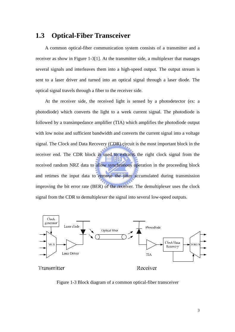
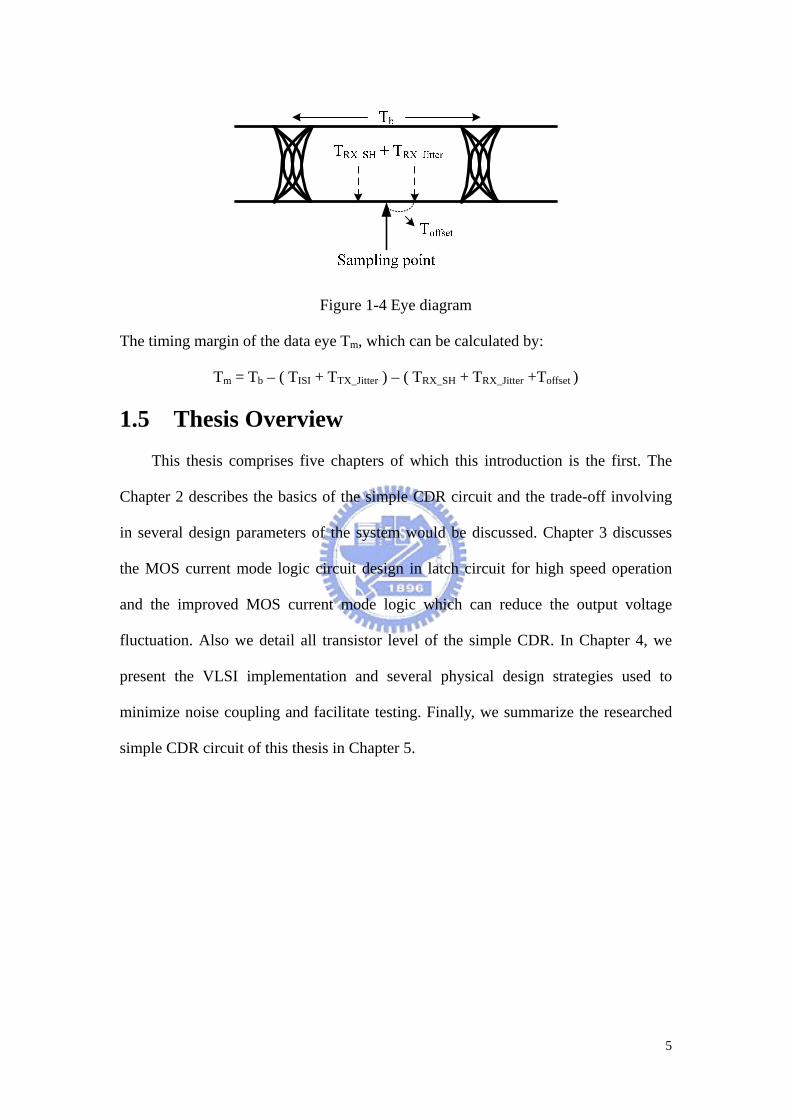
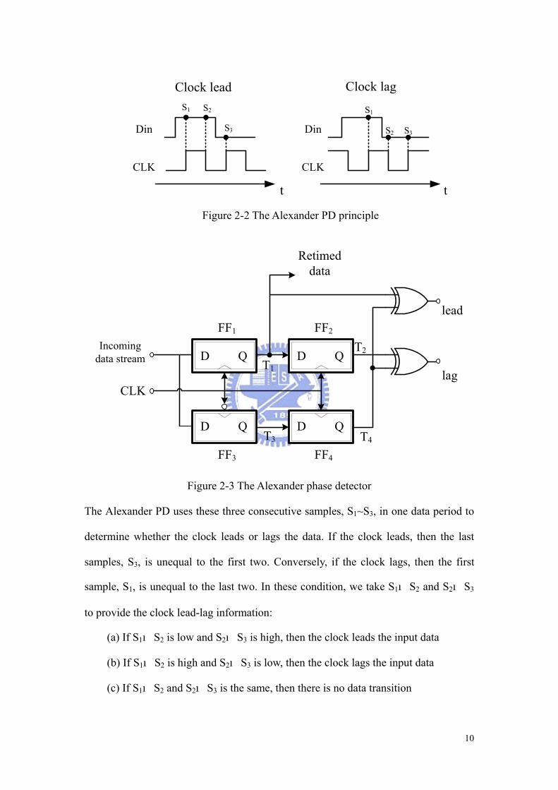
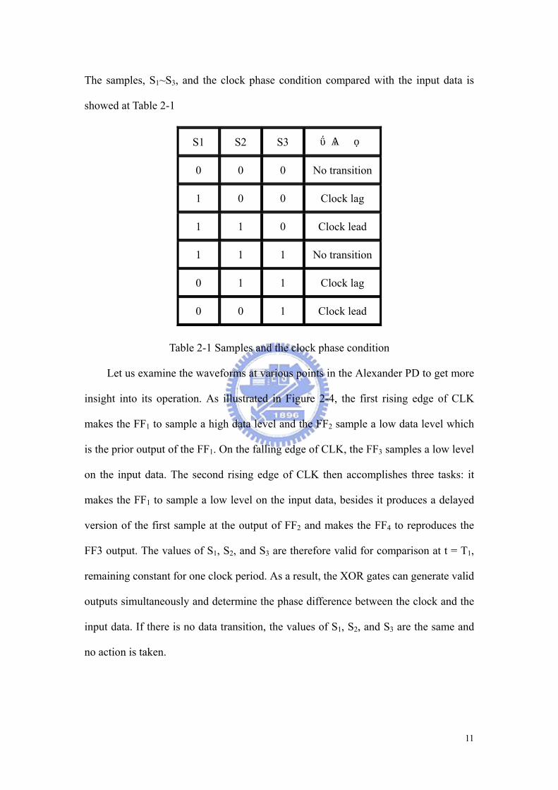
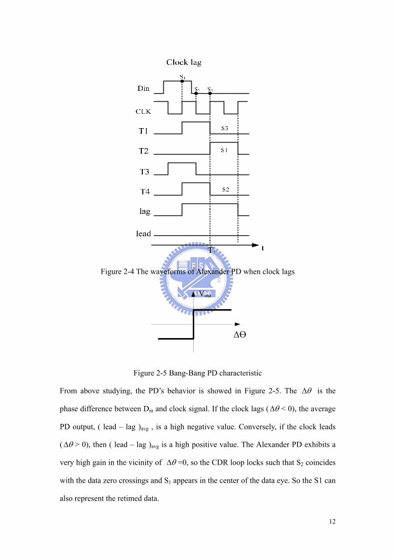
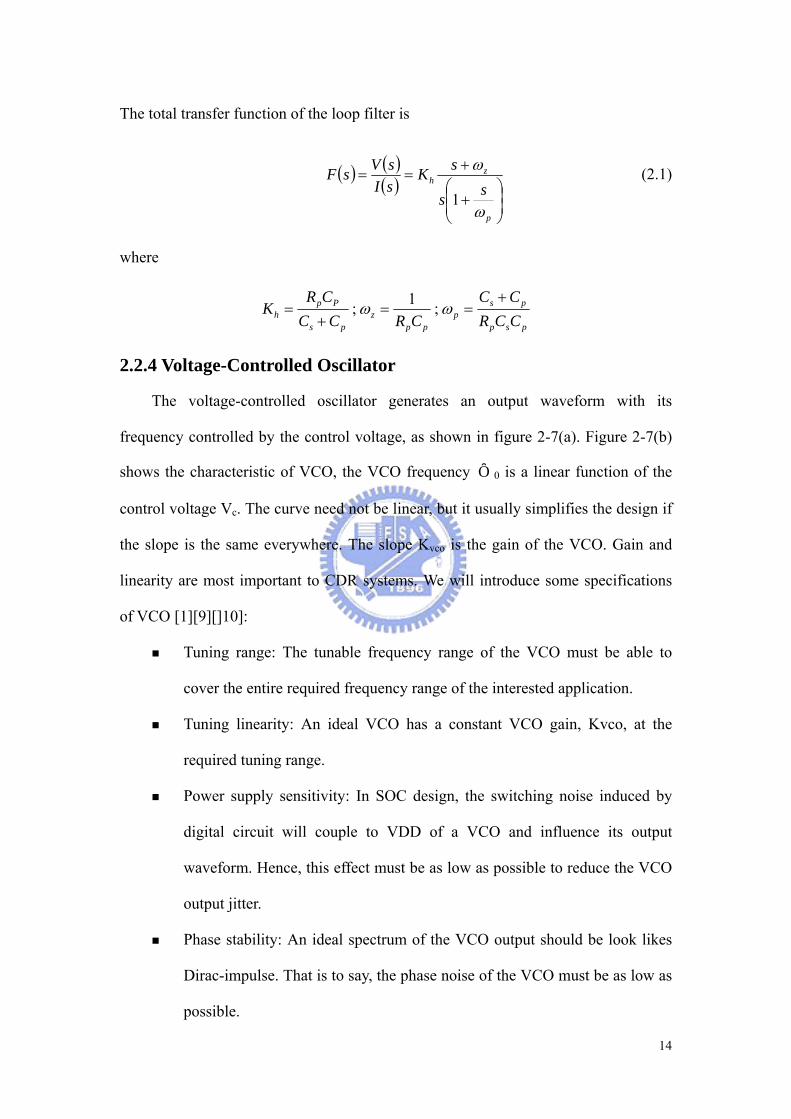
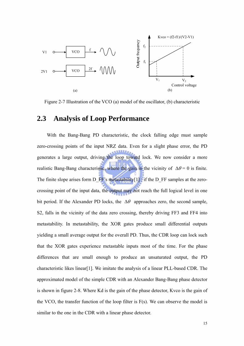
VCO
VCO
V1
2V1
f
2f
(a)
f1
f2
V1 V2
Kvco = (f2-f1)(V2-V1)
(b)Control voltage
Figure 2-7 Illustration of the VCO (a) model of the oscillator (b) characteristic
23 Analysis of Loop Performance
With the Bang-Bang PD characteristic the clock falling edge must sample
zero-crossing points of the input NRZ data Even for a slight phase error the PD
generates a large output driving the loop toward lock We now consider a more
realistic Bang-Bang characteristic where the gain in the vicinity of θ∆ = 0 is finite
The finite slope arises form D_FFrsquos metastability[1] if the D_FF samples at the zero-
crossing point of the input data the output may not reach the full logical level in one
bit period If the Alexander PD locks the θ∆ approaches zero the second sample
S2 falls in the vicinity of the data zero crossing thereby driving FF3 and FF4 into
metastability In metastability the XOR gates produce small differential outputs
yielding a small average output for the overall PD Thus the CDR loop can lock such
that the XOR gates experience metastable inputs most of the time For the phase
differences that are small enough to produce an unsaturated output the PD
characteristic likes linear[1] We imitate the analysis of a linear PLL-based CDR The
approximated model of the simple CDR with an Alexander Bang-Bang phase detector
is shown in figure 2-8 Where Kd is the gain of the phase detector Kvco is the gain of
the VCO the transfer function of the loop filter is F(s) We can observe the model is
similar to the one in the CDR with a linear phase detector
15
Figure 2-8 Model of the CDR
We first consider the open-loop response to obtain considerable insight into the design
of the CDR circuit This response can be derived by breaking the loop at the feedback
input of the phase detector The output phase ( )soθ is related to the input phase
( )siθ by
( ) ( ) ( )s
KsFKss VCOdio sdotsdotsdot= θθ (22)
The open-loop response H(s) then is given by
( ) ( )( ) ( )
sKsFK
sssH VCO
di
o sdotsdot==θθ (23)
We use the loop filter in Figure 2-6 then Eq (23) becomes
( )
⎟⎟⎠
⎞⎜⎜⎝
⎛+
+sdot=
⎟⎟⎠
⎞⎜⎜⎝
⎛
+sdotsdot
+
sdotsdot+sdot
+sdot
=
p
z
ps
spp
pp
ps
VCOd
ss
sK
CCCCR
ss
CRsCC
KKsH
ω
ω111
1
22
(24)
16
Where is the loop bandwidth of the CDR VCOhd KKKK sdotsdot=
Figure 2-9 shows the bode plot of the transfer function We can see the phase of H(s)
is -180o at ω= 0 and the zero ωz introduce the phase shift of +90o and the pole ωp
introduce the phase shift of -90o The phase margin could be described as follows
⎟⎟⎠
⎞⎜⎜⎝
⎛minus⎟⎟
⎠
⎞⎜⎜⎝
⎛= minus
pZ
KKPMωω
tantan 1 (25)
Another way to approximate this parameter is to ignore the shunt capacitor Cs Since
Cp gtgt Cs the zero PP
z CR1
=ω is much smaller than the pole ps
psp CCR
CCsdotsdot
+=ω
Hence Eq (24) can be re-written as
( ) 2
1s
CRsCKKsH p
p
VCOd sdotsdot+sdot
sdot= (26)
where ( )pCs
RsFsdot
+=1
|H(s)| H(s)
0dB
ωz ωp-180o
Phase Margin
Figure 2-9 Bode plot of the open-loop transfer function
17
For the CDR to be stable the following condition should hold
VCOd
p
pp KKC
CR sdotlt
sdot1 (27)
To consider the examples quoted above this design guarantees that the phase margin
is good enough to the loop[10][12]
231 approximated frequency response with Loop filter
In contrast to the approximated analysis above the other popular method to
analysis a CDR is by the closed-loop transfer function which is written is written is in
Eq (28) and loop filter transfer function is approximated to ( )p
p CsRsF
sdot+=
1
( ) ( )
( ) ( )( )( ) ( ) VCOdi KsFKssHs
sGsdotsdot+
VCOdo KsFKsHs sdotsdot=
+==
1θθ (28)
or equivalently by
( ) ( )( )
( )( )
12
12
1 2
+⎟⎟⎠
⎞⎜⎜⎝
⎛sdotsdot+⎟⎟
⎠
⎞⎜⎜⎝
⎛
+⎟⎟⎠
⎞⎜⎜⎝
⎛sdotsdot
=+
==
nn
n
i
o
ss
s
sHsH
sssG
ωξ
ω
ωξ
θθ (29)
where ξ define as the damping factor is given by
z
Kω
ξ21
= (210)
and nω define as the natural frequency (rads) is given by
18
zn K ωω sdot= (211)
The damping factor and natural frequency characterize the close-loop response The
close-loop frequency response of the CDR for different values of damping factor are
normalized to natural frequency as shown in Figure 2-10 This figure shows that the
CDR is a low-pass filter to the phase noise at frequency below nω For small value of
ξ the curve is shaper than those of large value of ξ In the CDR design the loop is
designed to be over-damping(ξ gt1) to avoid the jitter peaking effect This also helps
increase the phase margin of the open-loop transfer function
Magnitude(db)
Frequency(Hz)
Figure 2-10 The close-loop frequency response of the CDR
Figure 2-11 shows the transient step response of the CDR for different value of
damping factor and for time normalized to nω
1 The step response is generated by
instantaneously advancing the phase of the input by one radian and observing the
output for different damping levels in the time domain The CDR output initially
responses rapidly but takes a long time to the steady state for the damping factor
larger than one ie the system is over-damped We can find that the rate of the initial
response increase and the rate of the final response decrease That is a tradeoff in the
19
CDR design
S(t)
Figure 2-11 The close-
Time ( 10us)
loop transient step response of a CDR
20
Chapter 3
10 Gbs Clock and Data Recovery
Circuit Design
31 Introduction
This Chapter discusses the circuits design more detailed in transistor level The
design method could be applied to a CDR with the input data rate of 10 Gbs The
process and model used for the circuit design is the TSMC 018 microm 1P6M CMOS
process We simulate the CDR with HSPICE to acquire the detail electrical behavior
Moreover the process variations and the temperature effects should be taken into
account We must simulate the CDR in high temperature slow process and fast
process besides the normal temperature and typical process After that the post-layout
simulation including the circuit parasitic resistances and capacitances must be
simulated
32 Circuit Description
For the CDR circuit to handle high-frequency signals the circuit must have fast
switching speed ICs operating at speeds greater than 10 Gbs usually use GaAs
MESFETs GaAs HBTs Si BiCMOS transistors The power consumption of these
processes however is relatively large because their supply voltage is high and their
penetration current is large In the last years ICs are required to work at low power
21
and highly integrated for low cost The CMOS transistors have the advantages of low
power consumption and low cost but they still rarely been used in high-speed systems
because of their operation speed is too low
321 High speed MCML Latch
Generally a conventional CMOS inverter exhibits some drawbacks that prevent
it from being vastly used in high-speed low voltage circuits First a CMOS inverter is
essentially a single-ended circuit In a multi-gigahertz frequency range the short
on-chip wires act as coupled transmission lines The electromagnetic coupling thus
causes serious operational malfunctioning in the circuits particularly single-ended
circuits Beside the pMOS transistor in a static CMOS inverter will severely limit the
maximum operating frequency of the circuit For circuit can correctly operate at
10GHz domain we use the MOS current-mode logic (MCML) to take the place of
conventional CMOS logic MCML circuits can operate with lower signal voltage and
higher operating frequency at lower supply voltage than static CMOS circuits The
MCML has extensively used to implement ultrahigh-speed buffers [13] [14] latches
[14] multiplexers and demultiplexers [15] and frequency dividers [16]
Figure 3-1 shows inverters of the CMOS logic and the conventional MCML The
CMOS logic has the advantage of low power consumption but its operation is relative
slow For example the maximum toggle frequency of a conventional 018 μm
CMOS inverter is only about 35 GHz The power consumption of this CMOS logic is
the product of the operation frequency and the charging and discharging power per
unit switching On the other hand the power consumption of the MCML is the drain
current of the current source transistor MNb Therefore the power consumption of the
MCML is nearly independent of the operation frequency The CMOS logic uses
power only when charging and discharging its power consumption is generally
22
smaller than that of the MCML However in the gigahertz frequency range the power
consumption of the CMOS logic become larger than that of the MCML as shown in
Figure 3-2 [15] This means that the MCML is more suitable for low-power operation
in the gigahertz frequency range
Figure 3-1 Inverter circuits of the (a) CMOS logic and (b) MCML
Figure 3-2 Power consumption of the MCML and CMOS logic
A MCML latch consists of an input tracking stage MN1 and MN2 utilized to
sense and track the data variation and a cross-coupled regenerative pair MN3 and
23
MN4 being employed to store the data Figure 3-1 demonstrates a CMOS CML latch
circuit
Figure 3-3 Circuit schematic of a CMOS CML latch
The track and latch modes are determined by the clock signal inputs to a second
differential pair MN5 and MN6 When the signal CK is ldquohighrdquo the tail current Iss
entirely flows to the tracking circuit MN5 and MN6 thereby allowing Vout to track
Vin In the latch-mode the signal CK goes low the tracking stage is disabled whereas
the latch pair is enabled storing the logic state at the output
To achieve the best performance in a MCML latch a complete current switching
must take place and the current produced by the tail current needs to flow through the
ON branch only So the latch output voltage swing of single end is (RSSD IR sdot D is the
equivalent resistance of MP1 or MP2 when it is worked at linear region) The value of
load resistance depends on both the tail current and voltage swing requirement
Reducing the load resistance RD and increasing tail current Iss is one way to lower the
transient time without changing the output swing voltage but increasing the tail
current will also increase the power consuming The sizes of pair transistors
(MN1-MN2 and MN3-MN4) are increased by increasing the tail current and also are
24
increased by reducing the magnitude of single ended swing voltage The sizes of the
other transistors (MN5 MN6 and MNb) have the effect of the tail current only For
high speed switching between MN1-MN2 and MN5-MN6 we let the size of the
transistor as large as possible On the other hand the increasing of the transistor size
will make the parasitic capacitance serious The parasitic capacitance will slow the
operation speed of the circuit We must get the best balance between the transistor size
and the parasitic capacitance for circuit performance
Unfortunately the transient output of MCML latch signals has serious level
fluctuation as show in Figure 3-4 with a 10Gbs input data stream It comes from the
clock signal changes During each transition from the sampling mode ( CK is high ) to
the latching mode ( CK is low ) the current tail of the cross-coupled pair must first
recharge the capacitances of the cross-coupled pair as it start drawing current from the
output nodes and changing the logic state Consequently the output nodes of the
MCML latch generate current spiking resulting in the large fluctuation of the output
nodes that can yield operation failure at high speed application In the design of latch
the problem of the serious output fluctuation becomes more serious as lowering the
voltage swing It is a kind of the barrier disturbing high speed gate design[17][18]
Figure 3-4 Voltage waveforms at the output of a MCML Latch
25
322 Improved High speed MCML Latch
In the previous the MCML latch has serious output fluctuation It comes from
the variation of the tail current density depending on level change of clock and input
data signal though the output nodes are keeping its level unchanged This typed of
latch cannot avoid it To reduce this problem we propose a simple approach to
improve the MCML latch The proposed circuit is showed in Figure 3-5 We add an
nMOS MN7 as another current source only for MN3-MN4 cross-couple pair The
added MN7 makes the cross-couple pair always on so when the latch changes form
sample mode to the latch mode the tail current Iss does not need to recharge the
capacitances of the cross-coupled pair This can reduce the current spiking of the
output nodes reducing the fluctuation Because the cross-couple pair is always on the
sample pair MN1-MN2 must have larger current than ID to change the state of the
cross-couple pair to trace the input data in sample mode Figure 3-6 shows the
simulation results of the improved MCML latch with a 10Gbs input data stream
Figure 3-5 The improved MCML latch
26
Figure 3-6 Voltage waveforms at the output of the improved MCML Latch
323 Alexander Phase Detector
The Alexander phase detector is composed of four D_type Flip-Flops and two
XOR gates
3231 D_type Flip-Flop
In the previous chapter an Alexander phase detector use the D Flip-Flops to
sample the input data or delay the sampling result by a clock or half a clock For
correct operation at 10GHz domain we use the improved MCML architecture which
is proposed in last section to realize the high speed D Flip-Flop Figure 3-7 shows the
Master-Slave D type Flip-Flop When clock is ldquohighrdquo the master latch holds the
sampling result for half a clock and the slave latch samples the master output Any
changes at input nodes can not influence the output When clock is ldquolowrdquo the slave
latch holds the sampling state of the sampling pair for another half a clock The
sampling result at clock rising edge holds for a clock period Because the CDR input
data is random binary sequence we input a rate of 10Gbs 27-1 PRBS pattern to the D
Flip-Flop with a clock signal that is locked to the input pattern The performance
comparison of the D Flip-Flop with MCML latch and improved MCML latch is
27
showed in Figure 3-8(a) (b) We make eye diagram of the D Flip-Flop output to be
more clear about the performance of the MCML latch and the improved MCML latch
Table 3-1 shows the post simulation result of the two type D Flip-Flops
Figure 3-7 The Master-Slave D Flip-Flop
Figure 3-8(a) The Eye diagram of the D Flip-Flop
Figure 3-8(b) The Eye diagram of the D Flip-Flop with improved MCML latch
28
MCML
D Flip-Flop
Improved MCML
D Flip-Flop
Improved
performance
Jitter (pk-pk) 31 ps 07 ps 343
Eye opening (mv) 368 mv 488 mv 33
Output fluctuation 137 mv 71 mv 93
Table 3-1 Post simulation result of the two type D Flip-Flops
3232 XOR gate
Figure 3-9 shows the common schematic of MCML XOR gate[19] The circuit
has a similar structure like latch However it has two symmetric differential pairs
MN1-MN2 and MN3-MN4 which deal with same input signal as _ΑminusΑ pair When
both A and B have the same logic level logic high or low either MN1-MN5 or
MN3-MN6 turns on Consequently the output node Q goes logically low When two
input signals have different logic level one is high and the other is low either
MN2-MN5 or MN4-MN6 turns on The output node goes logically low minus
Q
Figure 3-9 MCML XOR gate
29
It is important to note that the XOR gates in Figure 2-3 must provide the two
different inputs with symmetric load Otherwise differences in propagation delays
result in systematic phase offsets To reducing the unbalance effect of the load each
of the XOR gates is implemented as shown in Figure 3-10[20] The circuit does not
use the stacking stages so it provides perfect symmetry between the two inputs The
output is single-ended but the single-ended ldquoearlyrdquo and ldquolaterdquo signals produced by the
two XOR gates in the phase detector are sensed with respect to each other thus acting
as a differential drive for the Voltage-to-Current converter The operation of the XOR
circuit is as follows We set the Vref at the output common-mode level of the D
Flip-Flop preceding the XOR gate If the two inputs are identical one of the tail
currents flows through the transistor MP and the output voltage is low If the two
logical inputs are not equal then one of the input transistors on the left and one of the
input transistors on the right turns on thus turning the transistor MP off and the output
voltage is high
Figure 3-10 Symmetric XOR gate
30
Figure 3-11 shows the post simulation result of the Alexander phase detectorrsquos
transfer function which is composed of the proposed structure above This is
accomplished by obtaining the difference value of lead and lag signals with 10Gbs
input data rate The PD zero output voltage at a phase difference is approximately
65ps (013π) from the metastable point indicating that the systematic offset between
the data and the clock is very small
-10 -08 -06 -04 -02 00 02 04 06 08 10-30
-20
-10
0
10
20
30
PD
out
put v
olta
ge (m
v)
Phase difference(π)
Figure 3-11 The transfer function of the Alexander PD
324 VI converter and Loop filter
Figure 3-12 shows the VI converter and the loop filter The VI converter
compares the output voltage of the two XOR gates of the Alexander phase detector
and converts this voltage difference to current output The output current will charge
or discharge the loop filter to tune the VCO controlling voltage Unlike charge pumps
VI converters need not to switch after every phase comparison Therefore it does not
suffer from the dead-zone issue Without the stacking switch MOS the VI converter
can provide nearly rail-to-rail voltage swings for the oscillator control line[20][21]
31
Although the Bang-Bang CDR loop is in general a nonlinear time-variant system
it can only be assumed linear if the phase error is small The design of the loop filter
is based on a linear time-invariant model of the loop and is performed in continuous
time domain
Figure 3-12 VI converter and loop filter
325 VCO
A voltage control oscillator (VCO) is the most sensitive building block in a CDR
as far as supply and substrate noise is concerned Therefore careful design is needed
in order to reduce noise and frequency drift Although ring oscillator has wide tuning
range and excellence of integration with digital CMOS process it can not accomplish
high-frequency operation such as 10GHz or higher To accomplish high-frequency
operation we use the LC-tank oscillator The LC-tank oscillator has an excellent
phase noise performance with low power consumption because of a relatively high
quality factor This high-speed component was realized in expensive technologies
such as GaAs SiGe or bipolar before Now the low cost of CMOS technology due to
its paramount maturity and high integration density has pushed the designers to
realize low noise VCO for CMOS system on chip[1][22]
As shown in Figure 3-13[23] the complementary cross-coupled differential LC
structure was used to realize the fully integrated 10GHz domain low noise and low
32
power consumption oscillator under 18V supply voltage Fully differential operation
provides complementary outputs The using of pMOS and nMOS structure offers
higher transconductance for a given current which results in saving power and faster
switching of the cross-coupled differential pair[1][24]
Figure 3-13 The complementary cross-coupled differential LC VCO
The oscillation frequency of LC topologies is equal to ( )LCfosc π21=
suggesting that only the inductor and capacitor values can be varied to tune the
frequency and other parameters such as bias currents and transistor transconductances
affect negligibly Since it is difficult to vary the value of monolithic inductors
we simply change the tank capacitance to tune the oscillator The tunable capacitance
is called ldquovaracorrdquo In circuit design a reverse-biased pn junction or a MOSFET can
serve as a varactor The MOSFET varactor suffers from a large source-drain resistance
in the vicinity of minimum capacitance due to the low carrier concentration in the
channel so a simple modification which is called ldquoaccumulation-mode MOS
oscf
33
varactorrdquo resolves these difficulties Figure 3-14 shows the structure of pn junction
and accumulation-mode MOS varactor[1]
p+ n+
n-wellp-substrate
n+
n-wellp-substrate
n+
VGVS
(a) (b)
Figure 3-14 Structure of varactor (a) pn junction (b) accumulation-mode MOS
While used in both bipolar and CMOS technologies the pn junction varactors become
less attractive at low supply voltage VCO design for two reasons First pn junctions
suffer from a limited tuning range that trades with nonlinearity in the C-V
characteristic The junction capacitance can express as
m
B
R
O
V
CC
⎟⎟⎠
⎞⎜⎜⎝
⎛Φ
+
=
1var (31)
where Co is the zero-bias value VR the reverse-bias voltage ΦB the built-in potential
of the junction and m a value typically between 03 and 04 At low supply voltages
VR has a very limited range yielding a small range for Cvar and hence for fosc The
capacitance varies slowly under reverse bias and sharply under forward bias thereby
introducing significant nonlinearity in the VCO characteristic Second at low supply
voltages it becomes increasingly more difficult to select the oscillator common-mode
level and signal swings so as to avoid forward biasing the diodes The
accumulation-mode MOS varactor does not exhibit the above shortcomings The C-V
characteristic is illustrated in Figure 3-15 The MOS varactor should operate with
34
positive and negative biases so as to provide maximum dynamic range CmaxCmin
of 25 to 3 with This device comfortably tolerates both positive
and negative voltages allowing large VCO swings
VVVV SG 11 leminusleminus
Figure 3-15 The C-V characteristic of accumulation-mode MOS varactor
Monolithic inductors are typically realized as spiral structures The mutual
coupling between every two turns results in a relatively large inductance per unit area
Figure 3-16(a) shows the symmetric spiral structure and figure 3-16(b) shows the
equivalent circuit model[25][1]
w
2R
S
Nturn number(N=2)
(a) (b)
L Rdc
Rsub Rsub
CoxCox
Csub Csub
Cs
Figure 3-16 (a) Symmetric spiral inductor (b) circuit model of inductor
35
The definition of each parameter is listed below
L inductance Rdc metal series resistance Cs overlap capacitance between the spiral and the center tap under pass Cox oxide capacitance between the spiral and substrate Rsub silicon substrate resistance Csub silicon substrate capacitance
For a given inductance different combinations of line width number of turns and
outer dimension can be used leading to a large design space However the dc
resistance of the inductor Rdc often constrains the choice of these values In particular
the line must be sufficiently wide so that Rdc does not significantly limit the Q
Nevertheless increasing W yields a greater area and a larger capacitance for the
inductor These will increase the loss of inductance At high frequency the series
resistance of the wire is also influenced by the skin effect heavily Interestingly such
current distribution also changes the inductance value because the area and hence the
magnetic flux enclosed by each turn change[25]
At high frequency the passive components is a very important part because they
compose the core of VCO the resonant tank High quality factors and low parasitics
are necessary for both inductor and varactor in respect of the phase noise tuning
range and power consumption Thus accurate modeling especially at frequencies
above 10GHz may require electromagnetic field simulations Because we do not have
any experience of making an on-chip passive components we make use of TSMC
018μm RFIC 1P6M+ process which provides electrical behavior characteristics of
spiral inductor and varactor for design reference The operation speed follows the
synchronous optical network (SONET) OC-192 at the forward error-correction(FEC)
bit rates of 1071Gbs[26] The post-layout simulation transfer curve of VCO is show
in Figure 3-17 Table 3-2 collates the simulation result
36
00 02 04 06 08 10 12 14 16 18 20
940E+009
960E+009
980E+009
100E+010
102E+010
104E+010
106E+010
108E+010
110E+010
112E+010
TT SS FF
Out
put F
requ
ency
Control Voltage
Figure 3-17 Simulation result of the VCO
TT post simulation
FF post simulation
SS post simulation
Power supply 18 V 18 V 18 V 974 ~ 1114
GHz 984 ~ 1106
GHz 9467 ~ 1106
GHz VCO tuning range 650 MHzv 1 GHzv 15 GHzv
VCO output swing (Vpeak to peak) 1 V 128 V 815 mV VCO power consumption 125mW 151mW 865mW
VCO phase noise -103dBc1Mhz -103dBc1Mhz -104dBc1Mhz
Table 3-2 VCO post simulation result
326 Output Driver
A source follower circuit is used as an output driver in the chip for the
convenience of measurement as shown in Figure 3-18 It also shows that the output
level shift bond wire parasitic and the loading effect of 50Ω The output level shift
before the source follower is used to adjust the output dc level A source follower can
provide low output impendence and strong driving capacity The single-ended source
follower circuit output resistance is gm1 The output signal could be measured
off-chip The output loading includes pad parasitic capacitance bonding wire
37
inductance and the 50Ω loading effect[27]
Figure 3-18 Source follower output buffer
33 Simulation Result
The CDR system is simulated by HSPICE with the TSMC 018um model The
simple CDR successfully locks to 27-1 NRZ PRBS data The control voltage for the
VCO is shown in Figure 3-19 The loop locks to the input data within 55us The
control voltage ripple is within 15mv Figure 3-20 shows the retimed NRZ data and
the retimed clock at 1071GHz It shows that the loop can tolerate a slight frequency
offset which is much larger than the frequency variation between the VCO output and
input NRZ data and can lock under the noisy random data stream
Figure 3-19 CDR locking behavior
38
Input Data
Retimed Data
Clock
Figure 3-20 Retimed data and clock
Finally retimed data jitter of the CDR with the improved MCML latch is showed
in Figure 3-21 The eye diagram of the retimed data shows that the peak-to-peak jitter
of the retimed data is 75ps
Figure 3-20 The eye diagram of the retimed data with improved MCML latch
Figure 3-22 shows the retimed data jitter of the CDR with common MCML latch The
eye diagram of the retimed data shows that the peak-to-peak jitter of the retimed data
is 112ps Compared with the two eye diagrams the improved MCML latch can
reduce the retimed data jitter and has better eye opening than the common MCML
latch
39
Figure 3-21 The eye diagram of the retimed data with common MCML latch
40
Chapter 4
VLSI Implementation
41 Layout
In a high-speed mixed-mode circuit design significant attention must be paid to
physical layout both to avoid speed degradation and to minimize noise coupling In
addition testing issues must be considered in conjunction with layout floor planning
and pad placement
The whole chip layout of the CDR is shown in Figure 4-1 It can be seen that a
large area is occupied by the spiral inductor The spiral inductor is created by TSMC
018um RF inductor model Above the spiral inductor the VCO complement nMOS
and pMOS cross-couple pairs use the TSMC 018um RF MOS model to provide
precise simulation result The loop filter is provided off chip to reduce chip area The
top circuit block is the Alexander Phase detector circuit Below the PD block the left
block is the data output buffers and the right block is the two XOR gates and the VI
converter
Several physical design strategies used to minimize noise coupling and facilitate
testing are listed below
1 In order to avoid the substrate noise coupling form RF VCO block to sensitive
other circuit block the ground signal used by VCO block circuit is separate form
the other circuit ground
41
2 In order to reduce the noise coupling between each building block and also to
monitor individual current sank easily by each block There are three sets of supply
voltage One is for the output buffer and the level shift circuits one is for LC-tank
VCO and another is for PD circuit and VI converter circuits
3 In order to reduce noise coupling between each circuits every circuit has its guard
ring
4 The biasing circuit for each main block is also separated The allocation of biasing
circuits is the same as that of supply voltage
Xor amp VI converter
Phase detector
Output buffer
Cross-couple pairs
Level shift
Spiral Inductor
Figure 4-1 Chip layout of the CDR circuits
42
The proposed CDR circuit has been implemented in TSMC 018um 1P6M mixed
signal CMOS process with a supply voltage of 18V The total area of the chip is
105mm times 0797mm
42 Performance Summary
The performance summary of the proposed CDR with improved MCML latch is
given in Table 4-1 The parameters in the system design are listed The CDR
performance between using improved MCML latch and using common MCML latch
are also provided in this table
Table 4-1 Performance summary
Technology TSMC 018μm RFIC 1P6M+ process
Power supply 18V
Chip Size 105mm times 0797mm
Power consumption 130mw(including output buffers)
Input bit rate 1071GbS (OC-192)
Output bit rate 1071 Gbs
Kpd 75 radmV
Kvco 650 MHzv
VCO phase noise -103dBc1Mhz
Lock time lt 6us
Retimed jitter 75ps(peak-to-peak)
CDR Spec
Power 407 mw
CDR with common
MCML latch Retimed jitter 112ps(peak-to-peak)
43
44
Chapter 5
Conclusion and Future Research
The simple CDR circuit was presented in this thesis This is a first attempt by the
author and still has much room for improvement The simple CDR uses the proposed
MCML architecture to incorporate the Alexander phase detector The proposed
MCML architecture can reduce the output signal level fluctuation These realizations
may improve the jitter performance The techniques for high-performance CDR
design remain a challenging and a promising task
In Chapter 2 a simple CDR with Alexander phase detector is presented The
system behavior and loop performance have been analyzed The approximate
second-order model which imitates the analytical of linear PLL model was derived
to validate the stability and to assist in system parameters design
In Chapter 3 a 10GHz simple CMOS CDR circuit has been realized in 018μm
standard CMOS process In order to operate at high-speed frequency in the Gbs range
reliably we must use the MCML architecture circuit which can operate correctly with
smaller input signal voltage swing at high frequency We proposed an improved
MCML circuit which can reduce the output signal level fluctuation drawback of
original MCML We use the full-rate Alexander bang-bang phase detector for a phase
tracking state The output of phase detector drives a VI converter The VI converter
output charges or discharges the loop filter to tune the VCO control voltage which
45
change the VCO oscillating frequency Finally we compare the system performance
between the improved MCML latch system and the common MCML latch system
The proposed improved MCML latch can reduce the CDR jitter and has more opened
eye diagram than the common MCML latch
In Chapter 4 there are some discussions on the layout techniques The common
centroid layout structure is used to reduce layout mismatch Finally the CDR circuit
as presented in this thesis occupies a 105mm times 0797mm chip area in TSMC
018um 1P6M technology The total power consumption of this chip is about 130mw
under a 18V supply voltage (two output buffers included)
This CDR structure is quite fundamental With the proposed MCML latch we
can improve the common MCML circuit drawback to get a better jitter performance
In this proposed CDR circuit we can additionally add a frequency detection circuit in
the future research The frequency detection drives the VCO frequency toward the
desired value by a frequency-locked loop When the frequency error reaches a
sufficiently small value the PLL takes over and performs phase locking This
frequency detector can improve the typical PLL drawback of small capture range
especially if it operates with random data
46
Bibliography
[1] B Razavi ldquoDesign of Integrated Circuits for Optical Communicationrdquo
McGRAW-Hill 2003
[2] N Miki and K Okada ldquoAccess flexibility with passive double star systemrdquo IEEE
5th Conf OptHybrid Access Network Proc 1993
[3] K Yukimatsu and Y Shimazu ldquoOptical interconnections in switching systemrdquo
IEICE Trans Electron vol E77-C no 1 pp2-8 Jan 1994
[4] R Farjad-Rad ldquoA CMOS 4PAM Multi-Gbps Serial Link Transceiverrdquo PhD
Thesis Stanford University 2000
[5] H Djahanshahi C Andre and T Salama ldquo Differential CMOS Circuits for 622
MHz933 MHz Clock and Data Recovery Applicationsrdquo IEEE Journal of
Solid-Stae Circuits Vol 35 No 6 June 2000
[6] L Wu H Chen S Nagavarapu R Geiger E Lee and W Black ldquoA monolithic
125Gbs CMOS clockdata recovery circuit for fibre channel transceiverrdquo in Proc
IEEE ISCAS Vol2 pp 565-568 Orlando FL June 1999
[7] CR Hogge ldquoA Self-Correcting Clock Recovery Circuitrdquo IEEE J Lightwave
Tech Vol 3 pp 1312-1314 Dec 1985
[8] JDH Alexander ldquoClock Recovery from Random Binary Datardquo Electronics
Letters Vol 11 pp 541-542 Oct 1975
[9] J Savoj and B Razavi ldquoHigh-speed CMOS circuits for optical receiversrdquo Kluwer
Academic Publishers 2001
[10] Dan H Wolaver ldquoPhase-locked loop circuit designrdquo Prentice-Hall 1991
47
[11] J Lee and B Razavi ldquo A 40Gbs Clock and Data Recovery Circuit in 018um
CMOS Technologyrdquo IEEE Journal of Solid-State circuits Vol 38 No 12 Dec
2003
[12] PK Hanumolu M Brownlee K Mayaram and Un-Ku Moon ldquo Analysis of
charge-pump phase-locked loopsrdquo IEEE Transactions on circuits and systems Vol
51 No 9 Sep 2004
[13] K Iravani F Saleh D Lee P Fung P Ta and G Miller ldquoClock and data
recovery for 125Gbs Ethernet transceiver in 035um CMOSrdquo in Proc IEEE
Custom Integrated Circuit Conf May 2001 pp261-264
[14] H T Ng and D J Allstot ldquoCMOS current steering logic for low-voltage
mixed-signal integrated circuitsrdquo IEEE Trans VLSI Syst vol 5 pp301-308
Sept 1997
[15] A Tanabe M Umetani I Fujiwara K Kataoka M Okihara H Sakuraba T
Endoh and F Masuoka ldquo018um CMOS 10Gbs multiplexerdemultiplexer ICs
using current mode logic with tolerance to threshold voltage fluctuationrdquo IEEE J
Solid-State Circuits vol 36 pp 988-996 June 2001
[16] H D Wholmuth D Kehrer and W Simburger ldquoA high sensitivity static 21
frequency divider up to 19 GHz in 120 nm CMOSrdquo in Proc IEEE Radio
Frequency Integrated Circuits (RFIC) Symp June 2002 pp 231-234
[17] JK Shin TW Yoo and MS Lee ldquoDesign of half-rate linear phase detector
using MOS current-mode logic gates for 10Gbs clock and data recovery circuitrdquo
Advanced Communication Technology 2005 ICACT 2005 The 7th International
Conference Vol 1 pp205 ndash 210 Feb 2005
[18] P Heydari and R Mohanavelu ldquoDesign of Ultrahigh-speed Low-Voltage CMOS
CML Buffers and Latchesrdquo IEEE Transactions on Very Large Scale in
Integration(VLSI) Systems Vol 12 no 10 Oct 2004
48
[19] M Alioto and G Palumbo ldquoModeling and Optimized Design of Current Mode
MUXXOR and D Flip-Floprdquo IEEE transactions on circuits and
systems-IIANALOG AND DIGITAL SIGNAL PROCESS Vol 47 no 5 May
2000
[20] J Savoj B Razavi ldquoA 10-Gbs CMOS clock and data recovery circuit with a
half-rate linear phase detectorrdquo IEEE Journal of Solid-State Circuits vol 36
Issue 5 pp 761 ndash 768 May 2001
[21] J Lee and B Razavi ldquoA 40Gbs Clock and Data Recovery Circuit in 018um
CMOS Technologyrdquo IEEE Journal of Solid-State Circuits Vol 38 No 12 Dec
2003
[22] D Baek T Song E Yoon and S Hong ldquo8GHz CMOS Quadrature VCO Using
Transformer-Based LC tankrdquo IEEE microwave and wireless components letters
Vol 13 No 10 Oct 2003
[23] J Maget M Tiebout R Kraus ldquoMOS varactors with n- and p-type gates and
their influence on an LC-VCO in digital CMOSrdquo IEEE Journal of Solid-State
Circuits vol 38 Issue 7 pp 1139 ndash 1147 July 2003
[24] Y H Kao and MT Hsu ldquoTheoretical analysis of low phase noise design of
CMOS VCOrdquo IEEE microwave and wireless components letters Vol 15 No 1
January 2005
[25] TSMC 018um MIXED signal 1P6M+ SALICIDE 18V33V PCM
SPEC(T-018-MM-PC-001)
[26] J Cao M Green A Montaz K Vakilian D Chung KC Jun M Caresosa X
Wang WG Tan Y Cai I Fujimori and A Hairapetian ldquoOC-192 Transmitter
and Receviver in Standard 018um CMOSrdquo IEEE Journal of Solid-State Circuits
Vol 37 No 12 Dec 2002
49
[27] SW Yoon S Hong and J Laskar ldquo Efficiency enhanced and harmonic
suppressed differential VCO with novel buffer scheme using transformers for
IEEE 80211ardquo IEEE MTT-S Digest
[28] National Semiconductor LM117LM317ALM317 3-Terminal Adjustable
Regular Data Sheet National Semiconductor Inc 1997
50
Appendix A
Testing Strategies
The chip testing consists of three steps namely DC power supply and ground
print circuit board (PCB) layout and closed-loop CDR testing
Firstly the DC operating point is measured to make sure that all of the biasing
current and DC points are in the vicinity of the original designs Since the CDR
system has a high frequency LC-tank VCO we partition the DC power supply and
ground-reference net on the PCB into 2 parts to isolate the noise coupling Hence the
VCO and other circuit ground planes is separated on the PCB and connected by a
inductor This inductor shorts the DC voltage of the VCO and other circuits grounds
while preventing the high-frequency noise coupling The power supply and bias
voltage are generated by LM 317 adjustable regulators as show in Figure A-1[28]
The input of the regulator circuit is connected to a 6V battery instead of a general
power supply because the noise of general power supply is much larger than the
battery The regulator circuit is easy to use and could be predicted by the Equation
A1
21
21251 RIRRV ADJout sdotsdot⎟⎟
⎠
⎞⎜⎜⎝
⎛+sdot= (A1)
where the IADJ is the DC current that flows out of the adjustment terminal ADJ of the
regulator The capacitor C1 can be added to improve transient response at the output
The output of the regulators are bypassed on the PCB with another bypass filter
network then connected to the chip The bypassed filter network is composed of by
51
10uF1uF01uF and 001uF capacitors as shown in Figure A-2
Figure A-1 LM 317 regulator
Figure A-2 Bypass filter at regulator output
Measurement must performed with raw die mounted on the PCB to prevent the
parasitic effect of the package which is illustrated in Figure A-3(a) and the testing
PCB layout was shown in Figure A-3(b) High-frequency signal traces such as NRZ
NRZB R_CLK R_CLK R_NRZ and R_NRZB are mode as short as possible to
reduce signal exhaustion and the length of differential signal traces are made close to
each other reduce the parasitic clock skew Each high-speed traces use the
SMA(Surface Mount Adaptor) connector High-speed output lines can easily couple
the large output swing onto the sensitive input line Another challenge is in placing
the discrete components and terminations match to the chip to reduce associated
parasitic and signal reflections
52
Figure A-3(a) Off-chip bonding wire test
Loop filter
Bare Die
Retimed Data
VCO GND NRZ
Circuit GND Retimed Data_B
NRZB
R_CLK
Figure A-3(b) The tes
The testing schematic of the closed-loop C
to avoid the substrate noise coupling from V
blocks and thus degrade the jitter performance
the other circuit block ground The VCO tun
Spectrum Analyzer(Agilent E4440A PSA Serie
voltage generated by DC power supply(Agilen
non-return-to-zero fully differential input d
Generator( Agilent N4901B Serial BERT 135G
R CLKB
ting PCB
DR is shown in Figure A-4 In order
CO block to sensitive other circuit
the VCO ground is separated from
ing range can be measured by the
s Spectrum Analyzer) with the tuning
t E3610A power supply) The PRBS
ata is generated by the Pattern
bs) The input DC offset voltage and
53
voltage swing can be set by this instrument After the loop is locked the resulting
eye diagram is monitored by the Oscilloscope(Tektronix TDS6124C Digital Storage
Oscilloscope)
Figure A-4 Experimental test setup
We measure the CDR chip with above setup method The first important
parameter to test is the VCOrsquos tuning range The measurement of the VCO result is
showed in Figure A-5 The VCO tuning range is 90641GHz ~89532GHz It is not in
our required range We conjecture that the circuit layout has heavy parasitic
capacitance The heavy parasitic capacitance lowers the VCO oscillation frequency
and the ratio of the varactor capacitance to total capacitances Thus the VCO tuning
range is more smaller than simulation The signal spectrum is showed in Figure A-6
The signal power is about -40dBm and the VCO output spectrum is not pure The
signal power is too small to let the CDR system work correctly The failure of
experiment reminds us that the layout of the high-speed VCO circuit should be more
54
symmetrical to reduce high frequency signal coupling The LC-tank VCO should have
effective guard ring to cut off the noise coupling form the inductor and varactor
00 02 04 06 08 10 12 14 16 18894
896
898
900
902
904
906
908
measure resultFr
eque
ncy
(GH
z)
control voltage (V)
Figure A-5 VCO tuning range experimental result
Figure A-6 VCO signal power
55
In order to reduce the bond wire parasitic inductor the chip pad of the high
frequency signal should be arranged symmetrically As showed in Figure A-7 where
two transmission lines carry differential signals to the bond wire pads The bond wire
parasitic can be represented by L1 and L2 and mutual coupling between the inductors
M yields the following voltage drops across each
MsIsLIV
MsIsLIV
ininL
ininL+minus
minus+
+minus=
minus=
22
11
with L1=L2=LP and we have minus+ = inin II
( )( )sMLIV
sMLIV
PinL
pinL
+minus=
minus=minus
+
2
1
Figure A-7 Bond wire parasitic
The key observation here is that mutual coupling reduces the transient drop across
each inductor thus lowering the effective inductor that appears in each signal line At
10GHz domain the signal path characteristic likes transmission line The transmission
line whose length is a significant fraction of the wavelength of interest or equivalently
whose end-to-end delay is not negligible with respect to other time scales in the
environment Each resistance mismatch of connector will make signal reflection
which disturbs the original signal The testing PCB must be manufactured exactly by
special company instead of etching by yourself to have better circuit characteristic
56
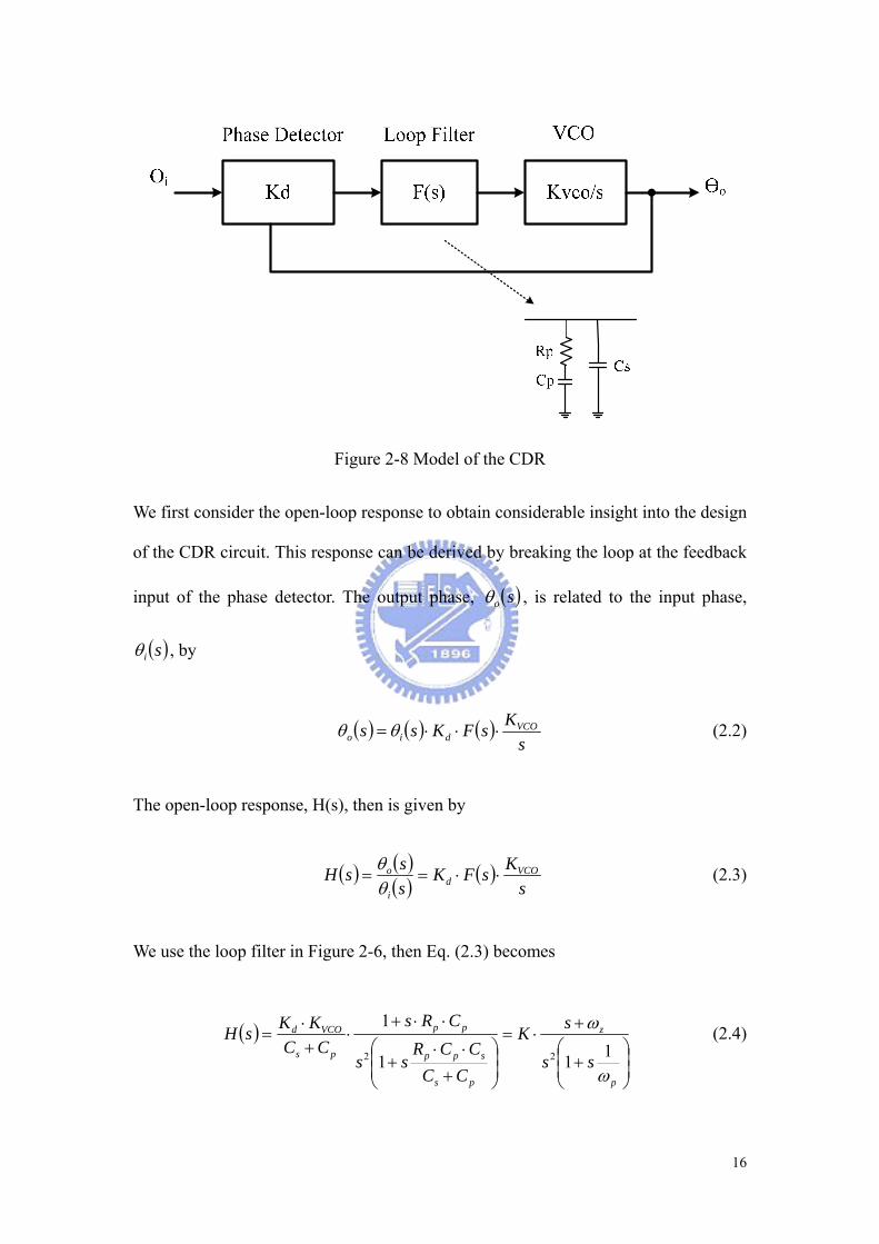
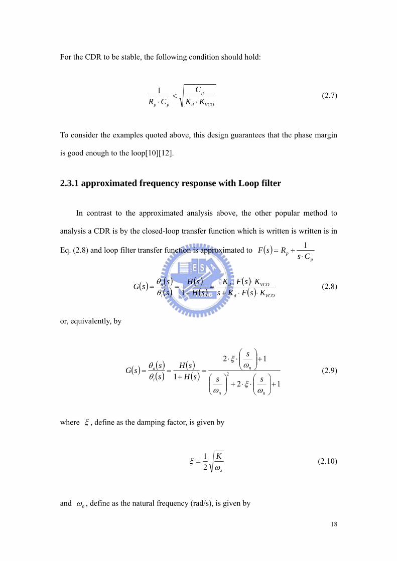
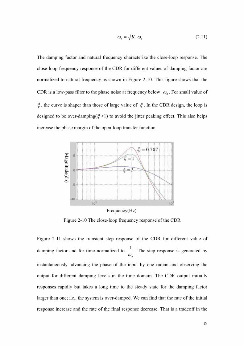
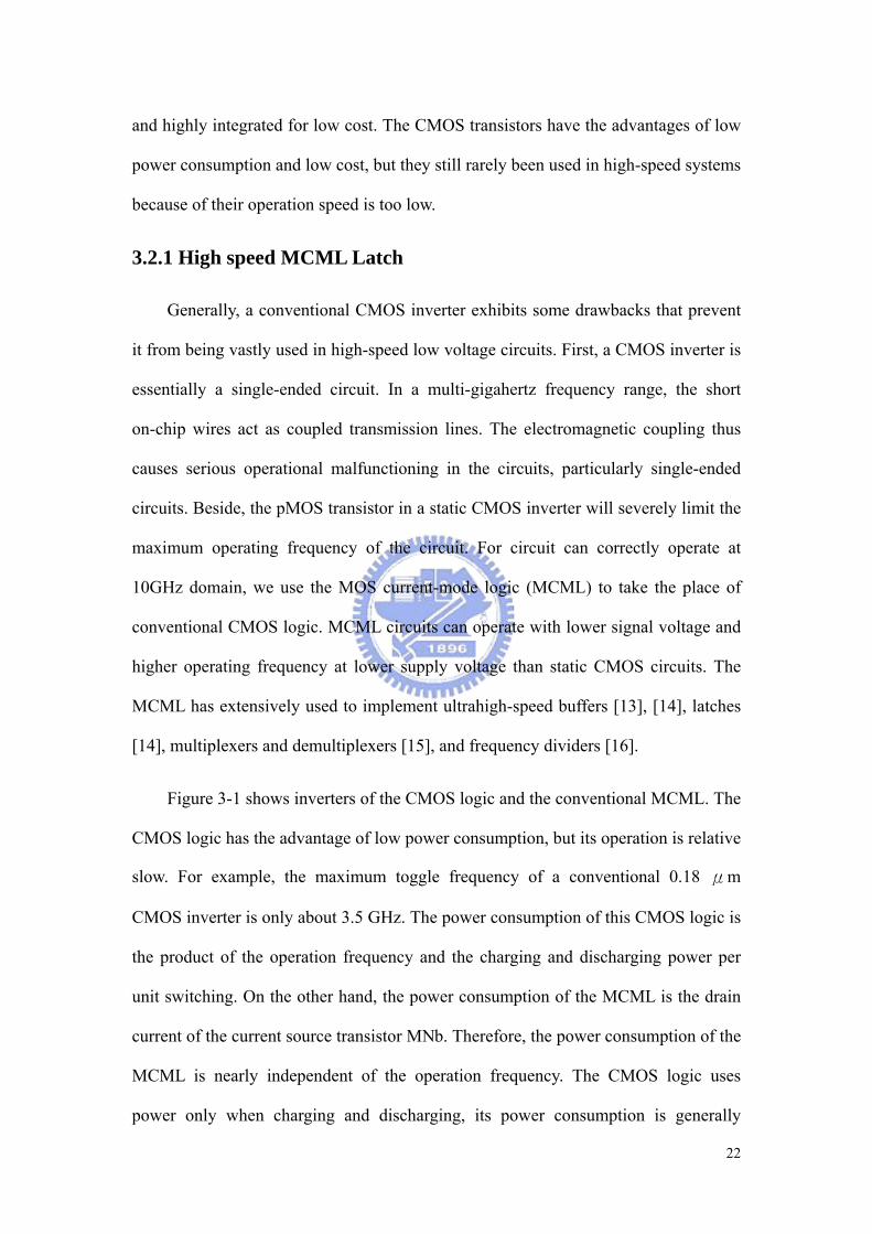
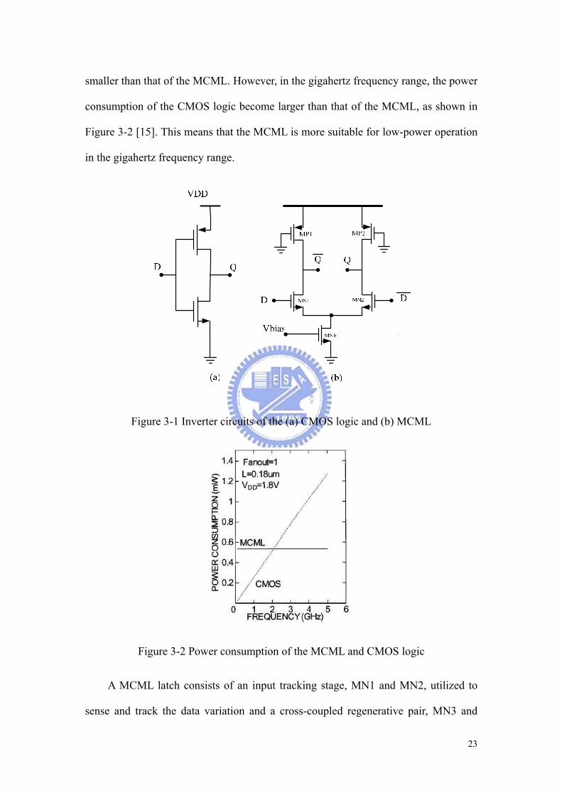
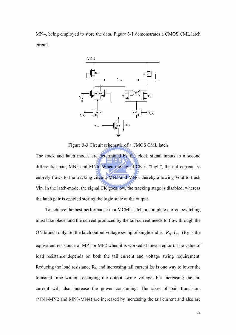
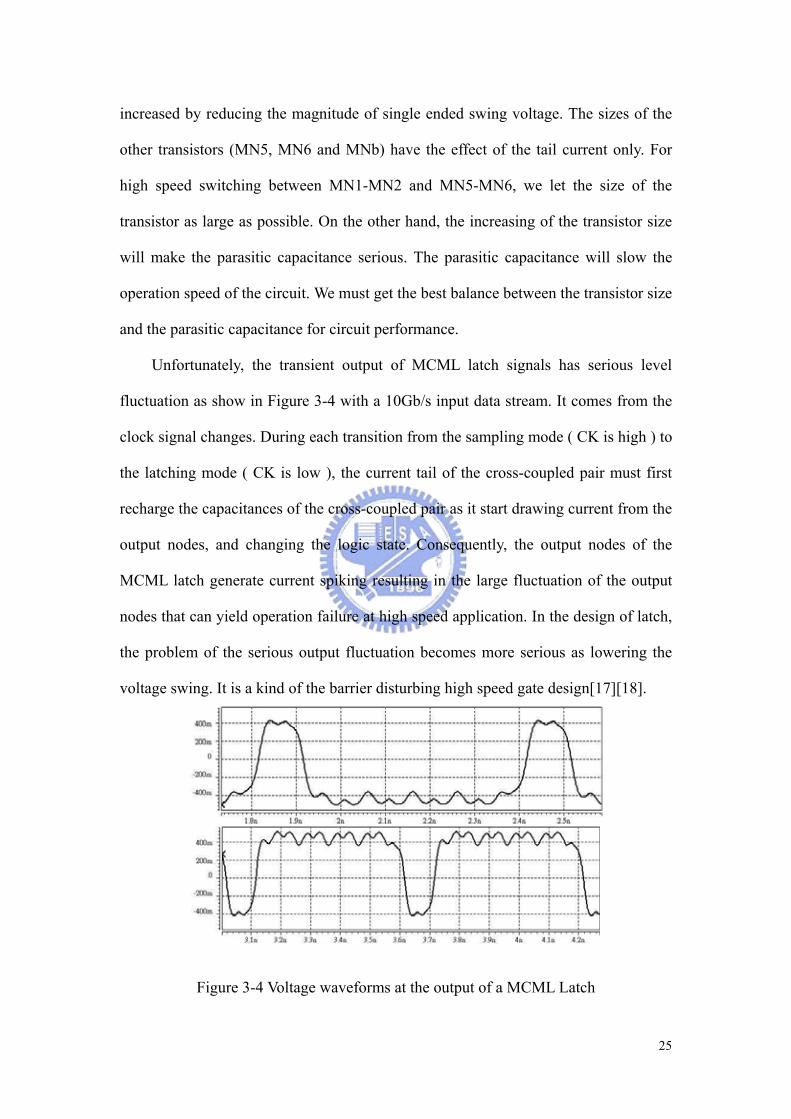
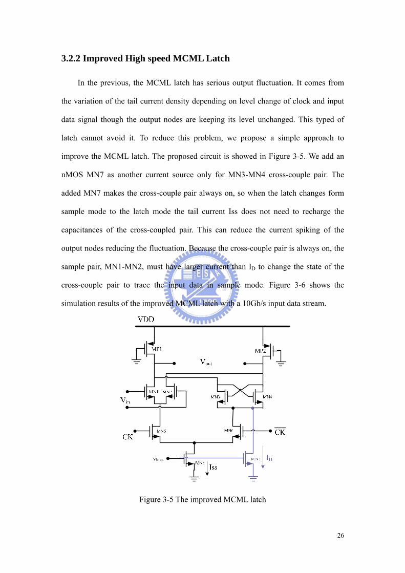
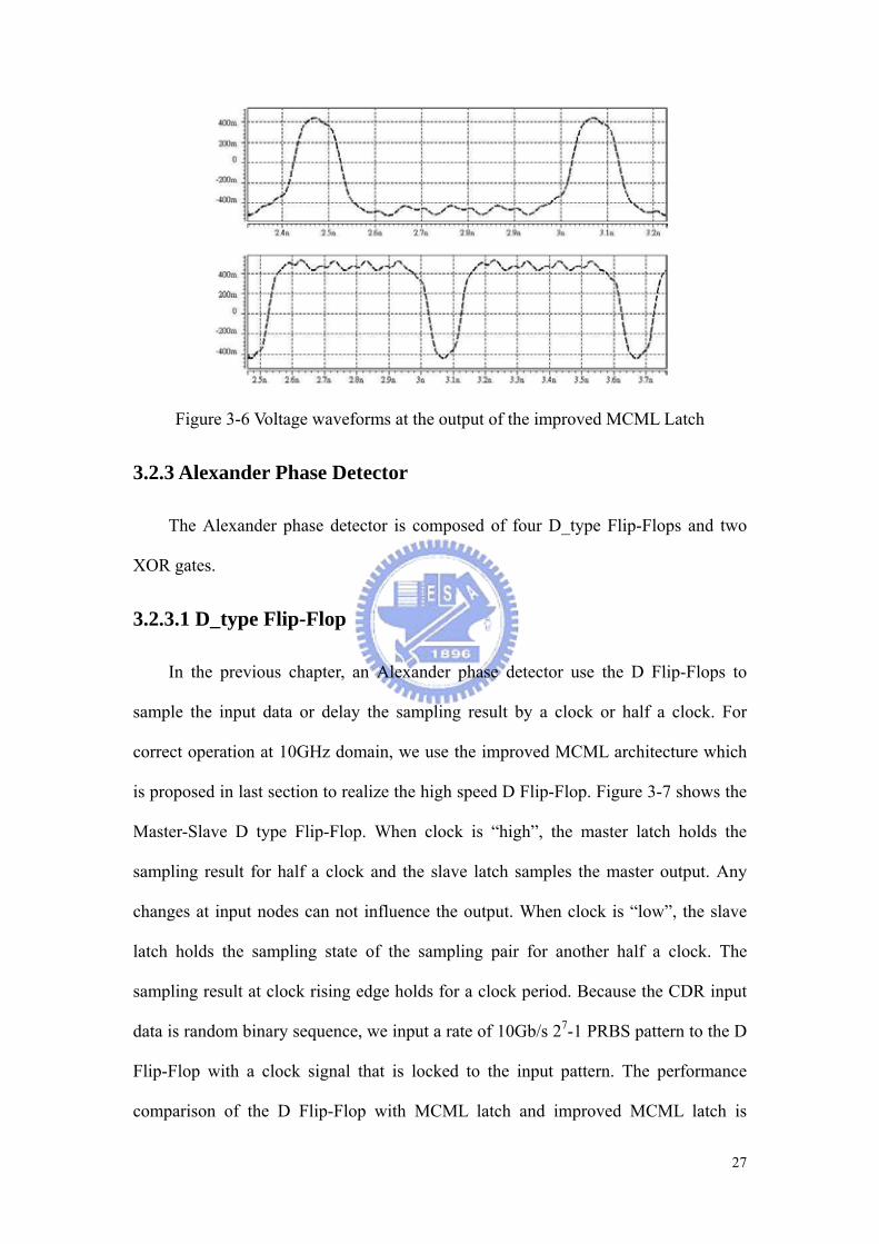
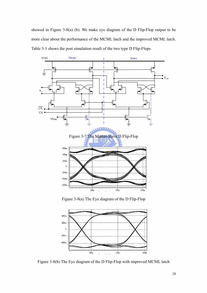
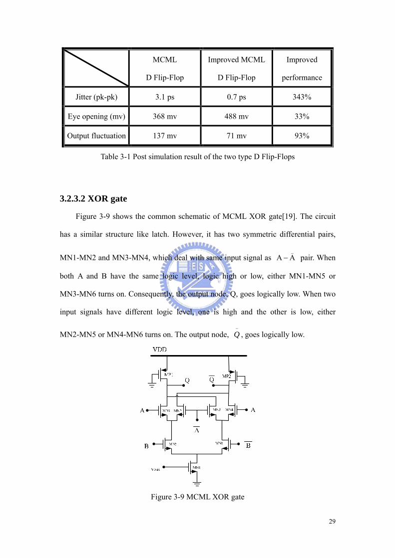
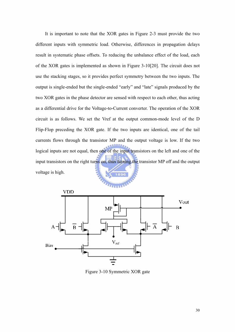
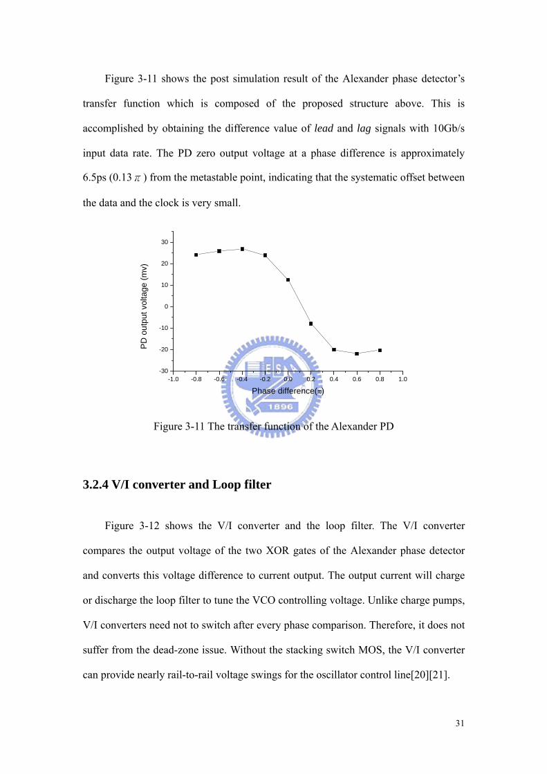
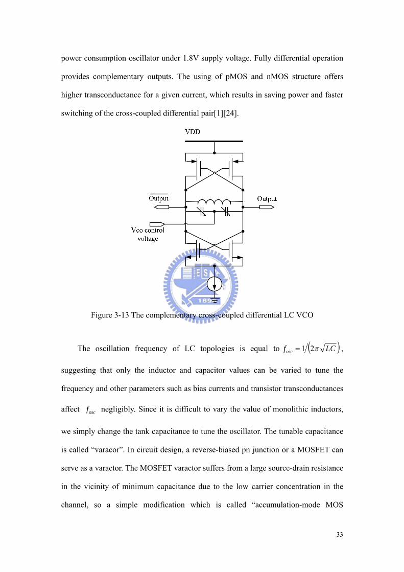
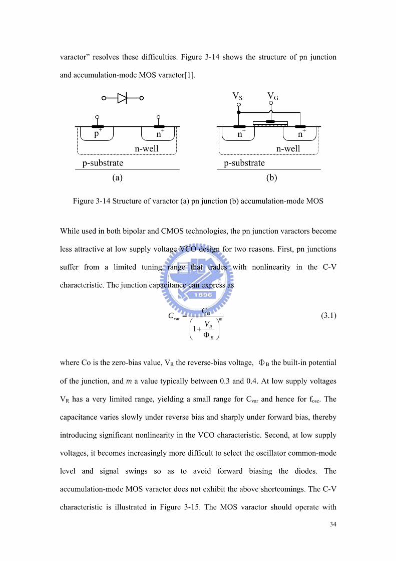
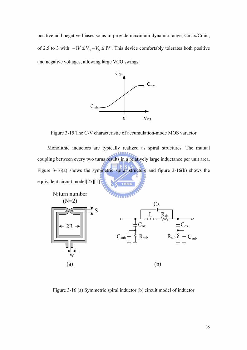
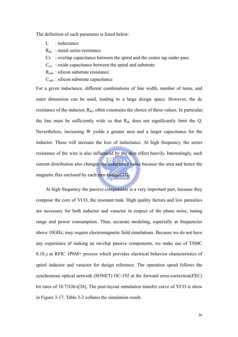
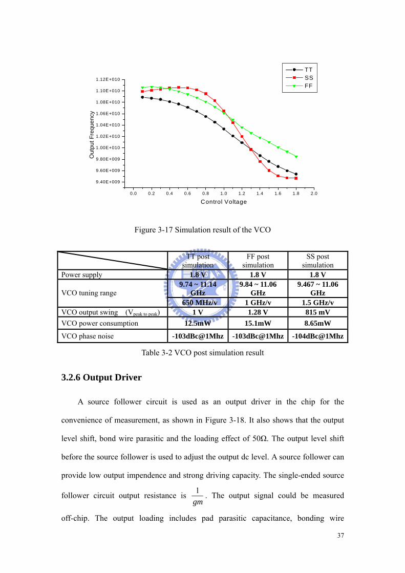
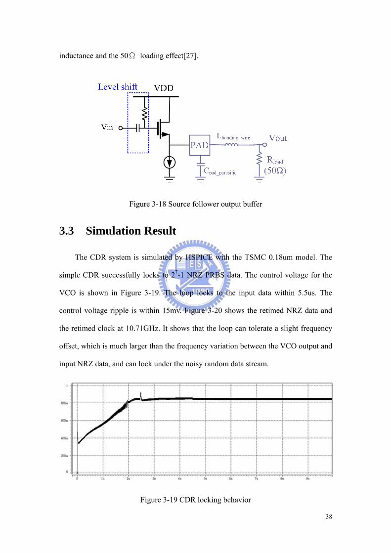
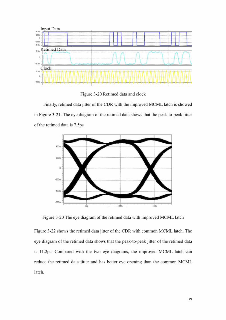
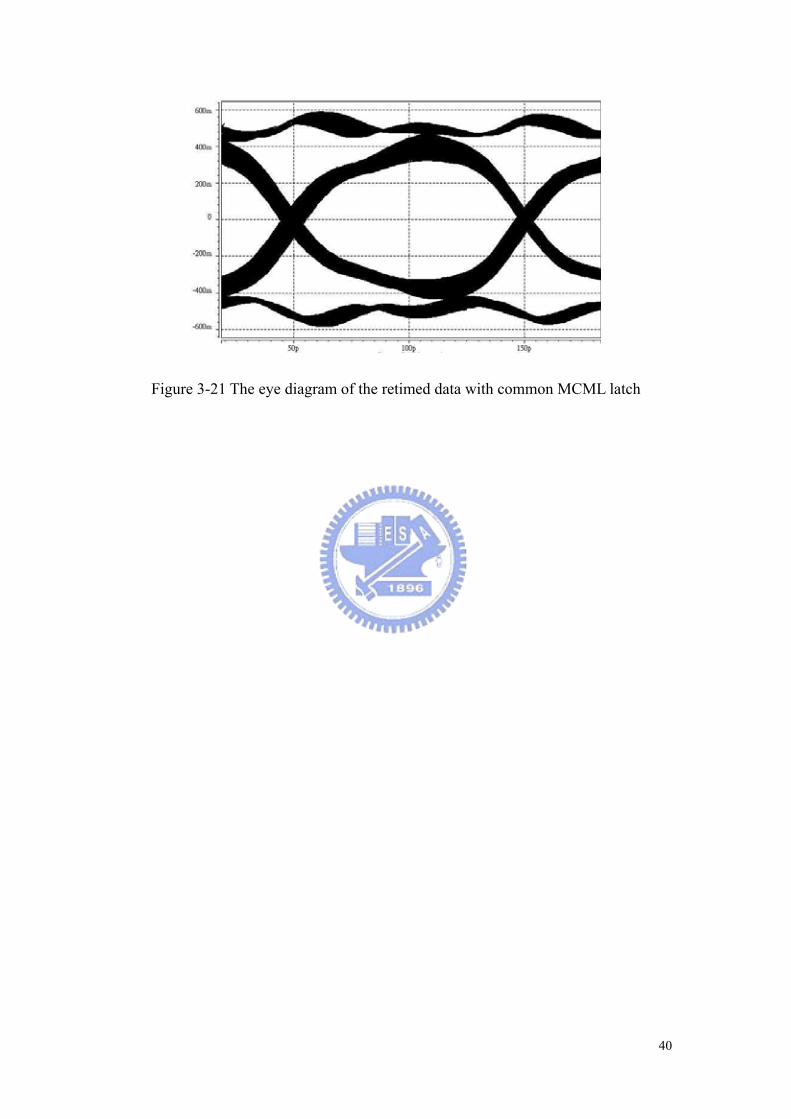
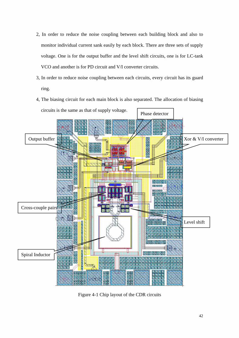
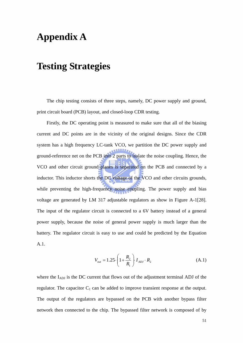
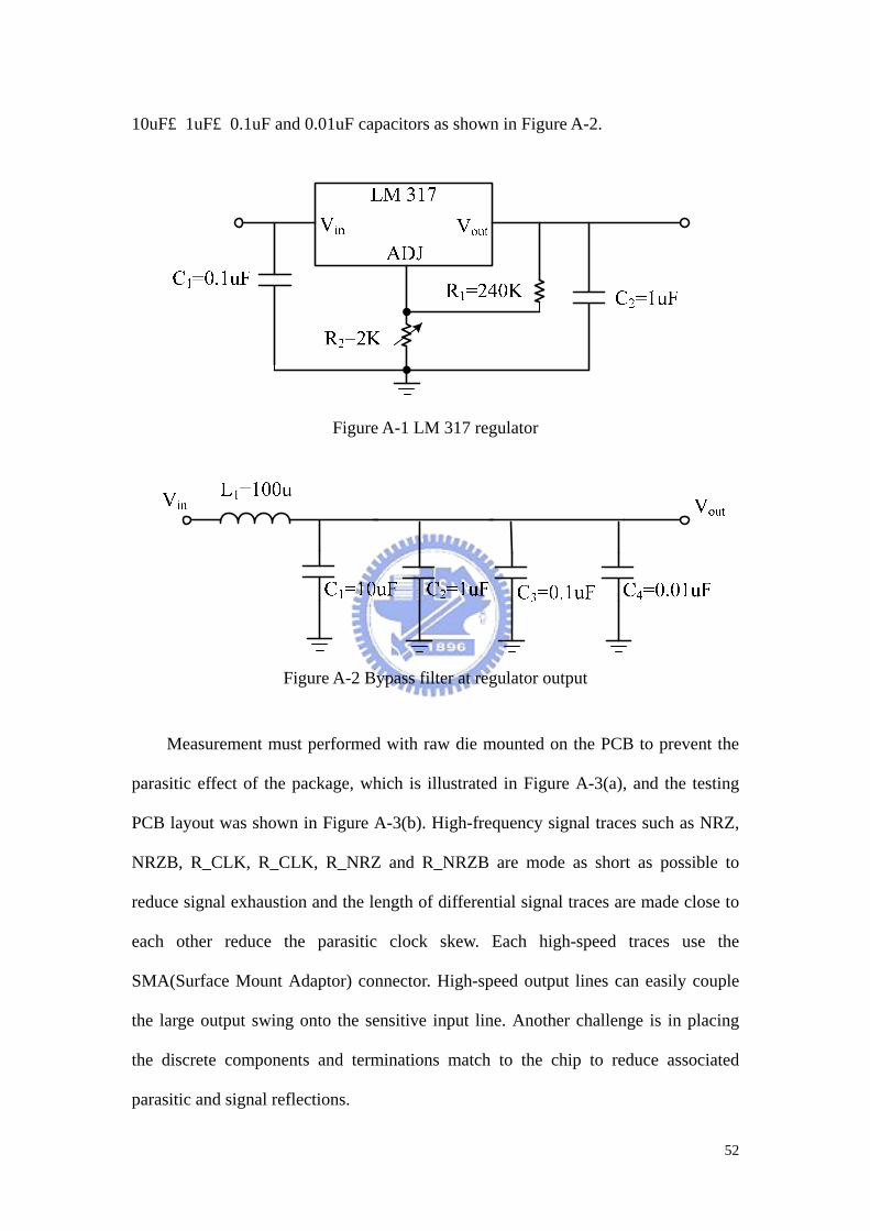
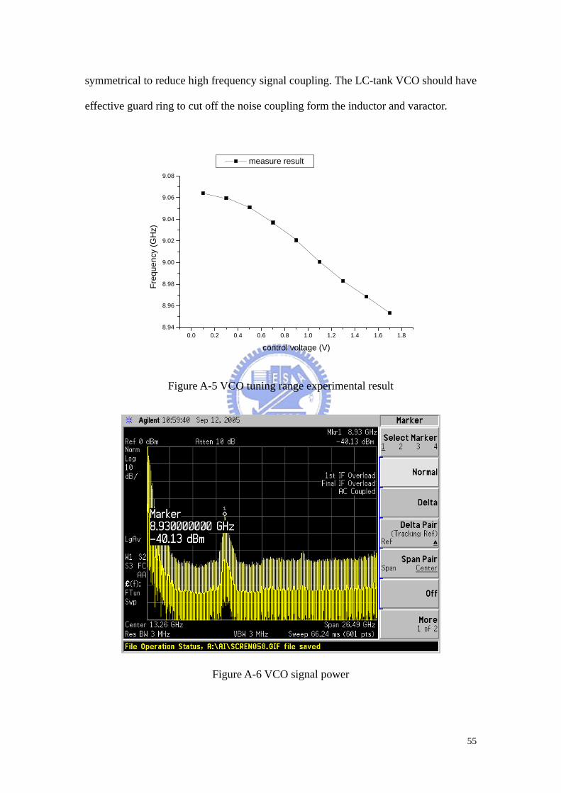
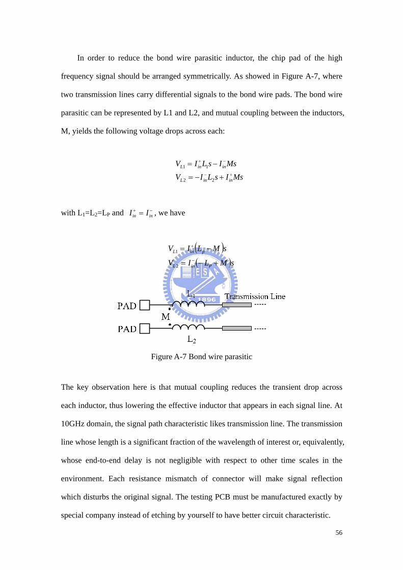