resistors taiseiohm
TRANSCRIPT
MKT-TAISEI Co.,Ltd.
Resistors TAISEIOHM
Thick Film Chip Resistor TSR
Thick Film SOP Resistor Networks THR-G
Thick Film Chip Resistor Networks TSR-N&W
Microwave Terminations TDR-3
Chip Terminations TCD-2, TCD-3
Tape & Reel Specifications
3
4-5
6
7
8-9
10-11
CONTENTS
e-resistors_contents03
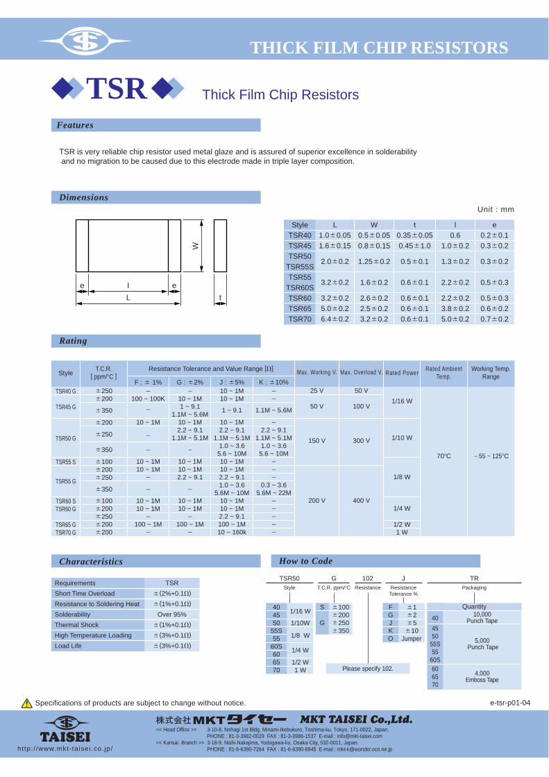
THICK FILM CHIP RESISTORS
Thick Film Chip Resistors
e-tsr-p01-04Specifications of products are subject to change without notice.
ht tp: / /www.mkt- ta isei .co. jp/
<< Head Office >> 3-10-8, Nohagi 1st Bldg, Minami-Ikebukuro, Toshima-ku, Tokyo, 171-0022, Japan. PHONE : 81-3-3982-0029 FAX : 81-3-3986-1537 E-mail : [email protected]<< Kansai Branch >> 3-18-9, Nishi-Nakajima, Yodogawa-ku, Osaka-City, 532-0011, Japan. PHONE : 81-6-6390-7264 FAX : 81-6-6390-6945 E-mail : [email protected]
Features
TSR is very reliable chip resistor used metal glaze and is assured of superior excellence in solderability and no migration to be caused due to this electrode made in triple layer composition.
DimensionsUnit : mm
StyleTSR40TSR45TSR50
TSR55STSR55
TSR60STSR60TSR65TSR70
L1.00.051.60.15
2.00.2
3.20.2
3.20.25.00.26.40.2
W0.50.050.80.15
1.250.2
1.60.2
2.60.22.50.23.20.2
t0.350.050.451.0
0.50.1
0.60.1
0.60.10.60.10.60.1
l0.6
1.00.2
1.30.2
2.20.2
2.20.23.80.25.00.2
e0.20.10.30.2
0.30.2
0.50.3
0.50.30.60.20.70.2
Ie et
W
L
Rating
Style Rated AmbientTemp.Rated PowerMax. Working V. Max. Overload V. Working Temp.
Range
TSR40 G
TSR45 G
TSR50 G
TSR55 S
TSR55 G
TSR60 STSR60 G
TSR65 GTSR70 G
1/16 W25 V
50 V
50 V
100 V
150 V 300 V
200 V 400 V
1/10 W
1/8 W
1/4 W
1/2 W1 W
70C 55 ~ 125C
Resistance Tolerance and Value Range []
F : 1%
100 ~ 100K
10 ~ 1M
10 ~ 1M10 ~ 1M
10 ~ 1M10 ~ 1M
100 ~ 1M
G : 2%
10 ~ 1M1 ~ 9.1
1.1M ~ 5.6M10 ~ 1M2.2 ~ 9.1
1.1M ~ 5.1M
10 ~ 1M10 ~ 1M2.2 ~ 9.1
10 ~ 1M10 ~ 1M
100 ~ 1M
K : 10%
1.1M ~ 5.6M
2.2 ~ 9.1
1.1M ~ 5.1M1.0 ~ 3.65.6 ~ 10M
0.3 ~ 3.65.6M ~ 22M
T.C.R.[ ppm/C ]
250200
350
200
250
350
100200250
350
100200250200200
J : 5%10 ~ 1M10 ~ 1M
1 ~ 9.1
10 ~ 1M2.2 ~ 9.1
1.1M ~ 5.1M1.0 ~ 3.6
5.6 ~ 10M10 ~ 1M10 ~ 1M2.2 ~ 9.11.0 ~ 3.6
5.6M ~ 10M10 ~ 1M10 ~ 1M2.2 ~ 9.1100 ~ 1M10 ~ 160k
Characteristics
RequirementsShort Time OverloadResistance to Soldering HeatSolderabilityThermal ShockHigh Temperature LoadingLoad Life
TSR(2%+0.1)(1%+0.1)
Over 95%(1%+0.1)(3%+0.1)(3%+0.1)
How to Code
TSR50Style
404550
55S55
60S606570
1/16 W
1/10W
1/8 W
1/4 W
1/2 W1 W
GT.C.R. ppm/C
S
G
100200250350
Please specify 102.
102Resistance
FGJKO
12510
Jumper
TRPackaging
4550
55S55
60S606570
40 10,000Punch Tape
5,000 Punch Tape
4,000Emboss Tape
Quantity
JResistance
Tolerance %
TSR
e-thr_g-p01-02_ai15
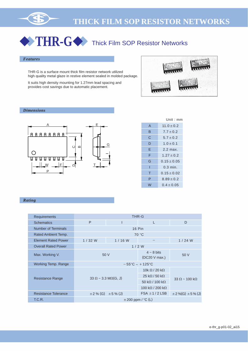
THICK FILM SOP RESISTOR NETWORKS
Thick Film SOP Resistor Networks
Features
THR-G is a surface mount thick film resistor network utilized high quality metal glaze in restive element sealed in molded package.
It suits high density mounting for 1.27mm lead spacing andprovides cost savings due to automatic placement.
Dimensions
Unit : mm
A
B
C
D
E
F
G
I
T
P
W
11.00.2
7.70.2
5.70.2
1.00.1
2.2 max.
1.270.2
0.150.05
0.3 min.
0.150.02
8.890.2
0.40.05
A
C BD
E
F
G
I
T
P
W
Rating
Requirements
Schematics
Number of Terminals
Rated Ambient Temp.
Element Rated Power
Overall Rated Power
Max. Working V.
Working Temp. Range
Resistance Range
Resistance Tolerance
T.C.R.
PTHR-G
16 Pin
1 / 2 W
55C ~ 125C
70 C
1 / 32 W 1 / 16 W 1 / 24 W
I L D
33 ~ 3.3 M(G, J)
2 % (G) 5 % (J)
200 ppm / C (L)
33 ~ 100 k
10k / 20 k
25 k/ 50 k
50 k / 100 k
100 k / 200 k
50 V4 ~ 8 bits
(DC20 V max.)50 V
FSA 1 / 2 LSB 2 %(G) 5 % (J)
THR-G

e-thr_g-p02-03Specifications of products are subject to change without notice.
<< Head Office >> 3-10-8, Nohagi 1st Bldg, Minami-Ikebukuro, Toshima-ku, Tokyo, 171-0022, Japan. PHONE : 81-3-3982-0029 FAX : 81-3-3986-1537 E-mail : [email protected]<< Kansai Branch >> 3-18-9, Nishi-Nakajima, Yodogawa-ku, Osaka-City, 532-0011, Japan. PHONE : 81-6-6390-7264 FAX : 81-6-6390-6945 E-mail : [email protected] tp: / /www.mkt- ta isei .co. jp/
THICK FILM SOP RESISTOR NETWORKS
Schematics
Voltage Divider
RA
RB
RA
RB
RA
RB
RA
RB
RA
RB
RA
RB
RA
RB
16 15 14 13 12 11 10 9
1 2 3 4 5 6 7 8
Parallel Circuit
1 2 3 4 5 6 7 8
16 15 14 13 12 11 10 9
Ladder Circuit
16 15 14 13 12 11 10 9GND
1
2R
R R R R R R R
2R 2R 2R 2R 2R 2R 2R
2R
2 3 4 5 6 7 8LSB
1 2 3 4 5 6 7 8
16 15 14 13 12 11 10 9
Isolated Circuit
Characteristics
Requirements
Short Time Overload
Temperature Cycling
Resistance to Soldering Heat
Withstanding Voltage
Moisture Resistance Load Life
Load Life
Terminal Strength
THRG(0.5 %0.05 )
(0.5 %0.05 )
(0.5 %0.05 )
(0.5 %0.05 )
(2.0 %0.05 )
(2.0 %0.05 )
(0.5 %0.05 )
Test method JIS C 5202
How to code
Voltage Divider
MConfigurations
M MINI-FLAT Please specify 102 or 1k.
GResistive Element
16Pins
102Resistance
JResistance
Tolerance [%]
T32Packaging
ISchematics
I
P
L
D
Isolated
Parallel
Ladder Circuit
G
J
2
5
M
T24
T32
Magazine
Emboss Tape Reel
Paper Tape
Magazine Case
Tape Reel
40
2,000
Quantity
G Thick Film
16 pinG
Number of Pins
e-tsr_n-p01-03Specifications of products are subject to change without notice.
ht tp: / /www.mkt- ta isei .co. jp/
<< Head Office >> 3-10-8, Nohagi 1st Bldg, Minami-Ikebukuro, Toshima-ku, Tokyo, 171-0022, Japan. PHONE : 81-3-3982-0029 FAX : 81-3-3986-1537 E-mail : [email protected]<< Kansai Branch >> 3-18-9, Nishi-Nakajima, Yodogawa-ku, Osaka-City, 532-0011, Japan. PHONE : 81-6-6390-7264 FAX : 81-6-6390-6945 E-mail : [email protected]
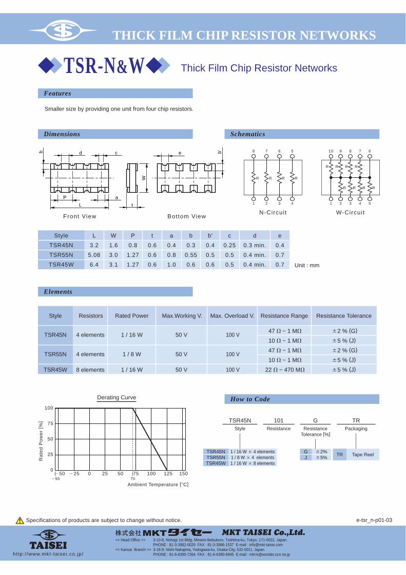
THICK FILM CHIP RESISTOR NETWORKS
Thick Film Chip Resistor Networks
Features
Smaller size by providing one unit from four chip resistors.
Dimensions
Unit : mm
Style
TSR45N
TSR55N
TSR45W
L
3.2
5.08
6.4
W
1.6
3.0
3.1
P
0.8
1.27
1.27
t
0.6
0.6
0.6
a
0.4
0.8
1.0
b
0.3
0.55
0.6
b'
0.4
0.5
0.6
c
0.25
0.5
0.5
e
0.4
0.7
0.7
d
0.3 min.
0.4 min.
0.4 min.
Front View Bottom View
b d c
P aL t
W
e b'
Schematics
R R R R
1 2 3 4
8 7 6 5
N-Circui t
R R R R
R R R R
1 2 3 4
10 89 7 6
5
W-Circui t
Elements
Style
TSR45N
TSR55N
TSR45W
Resistors
4 elements
4 elements
8 elements
Rated Power
1 / 16 W
1 / 8 W
1 / 16 W
Max.Working V.
50 V
50 V
50 V
100 V
100 V
100 V
Max. Overload V. Resistance Range
47 ~ 1 M
10 ~ 1 M
47 ~ 1 M
10 ~ 1 M
22 ~ 470 M
Resistance Tolerance
2 % (G)
5 % (J)
2 % (G)
5 % (J)
5 % (J)
125 150
100
75
50
25
050
5525 0 25 50 75
70100
Ambient Temperature [C]
Rat
ed P
ower
[ %]
Derating Curve How to Code
TSR45NStyle
TSR45NTSR55NTSR45W
1 / 16 W 4 elements1 / 8 W 4 elements1 / 16 W 8 elements
GResistance
Tolerance [%]
GJ
2%5% TR Tape Reel
TRPackaging
101Resistance
TSR-N&W

e-tdr_3-p01-05Specifications of products are subject to change without notice.
ht tp: / /www.mkt- ta isei .co. jp/
<< Head Office >> 3-10-8, Nohagi 1st Bldg, Minami-Ikebukuro, Toshima-ku, Tokyo, 171-0022, Japan. PHONE : 81-3-3982-0029 FAX : 81-3-3986-1537 E-mail : [email protected]<< Kansai Branch >> 3-18-9, Nishi-Nakajima, Yodogawa-ku, Osaka-City, 532-0011, Japan. PHONE : 81-6-6390-7264 FAX : 81-6-6390-6945 E-mail : [email protected]
MICROWAVE TERMINATIONS
Microwave Terminations
Features
TDR-3 ser ies provideds smal l conf igurat ions, wide frequency range and low pr ice by ut i l iz ingtantalum al loy wi th high heat resistance and alsoprovides cost reduct ion because the thermalresistance is low.
Applicable to MIL-R-11804
DimensionsUnit : mm
Style
3010
3030
3050
3150
L0.3
13.0
20.0
22.0
30.0
W0.5
5.0
5.8
8.0
18.0
E
1.6 (2.0)
2.5 (3.0)
2.5 (3.5)
4.5
H max.
2.5 (3.0)
4.0 (4.5)
4.5 (5.0)
6.0
P0.2
8.0
14.0
14.0
22.0
d
2.6
3.2
3.6
3.6
l1
3.0
5.0
5.0
10.0
w0.3
0.8
1.0
2.0
3.0
t
0.05
0.1
0.1
0.1
3003 (3 W)
3010 (10 W) 3030 (30 W)3050 (50 W) 3150 (150 W)
0.8
6.54.0
1.6
2.3
3.2
2.0 max.(2.5 max.)
0.9 (1.5)
3.0
0.05
HE
t
PL
w
Wl
2-d
Electrical Specifications
Impedance 100 is only for the B type. 300W is also available if required.
Rated Power
Frequency Range
V S W R
Impedance
Working Temp. Range
Resistance Tolerance
T.C.R.
Heat Resistance
3
DC ~ 5 (3) GHZ
4 <7> C/W
10
DC ~ 4 (2) GHZ
2 <4> C/W
30
DC ~ 2 (1.5) GHZ
1.8 <2.5> C/W
50
DC ~ 5 (1) GHZ
1.3 <2> C/W
150
DC ~ 0.8 (0.5) GHZ
50
200 ppm/C
0.5C/W
55 ~ 155 C5%(J) : Standard article, 2%(G), 1%(F)
1.2 max.
50, 100 (Type B only)
100 ppm/C
The numbers in ( ) of Frequency Range are values of the B type. The numbers in < > of Heat Resistance are values of 100 impedance type.
The numbers in ( ) are the dimensions of 100 type impedance.
Derating Curve100
75
50
25
050
5525 0 25 50 75 100 125 150
155654535
Ambient Temperature [C]
Rat
ed P
ower
[ %]
Other
3050B1003050B100
31503150
How to Code
TDRStyle
003010030050150
3 W10 W30 W50 W
150 W
FGJ
1%2%5%
50100
50100
3ID No.
010Rated Power
S
B
Type S
Type B
50Impedance
JResistanceTolerance
STerminals
TDR-3

CHIP TERMINATIONS
e-tcd2008-p01-06
http: / /www.mkt- ta isei .co. jp/
Specifications of products are subject to change without notice.
<< Head Office >> 3-10-8, Nohagi 1st Bldg, Minami-Ikebukuro, Toshima-ku, Tokyo, 171-0022, Japan. PHONE : 81-3-3982-0029 FAX : 81-3-3986-1537 E-mail : [email protected]<< Kansai Branch >> 3-18-9, Nishi-Nakajima, Yodogawa-ku, Osaka-City, 532-0011, Japan. PHONE : 81-6-6390-7264 FAX : 81-6-6390-6945 E-mail : [email protected]
TCD-2 Chip Terminations
Dimensions
Unit : mm
L
5.00.2
W
2.50.2
H
0.8 max.
T1
0.450.2
T2
3.00.2
T1T2
L
Input-Side Notation
HW
Bottom ViewSide ViewTop View
Rating
Requirements
Frequency Range
VSWR
Impedance
Resistance Tolerance
T.C.R.
Rated Power
Working Temp. Range
TCD-2008B50J
DC ~ 2.5 GHz
1.2 max.
50 5 %
100 ppm/C
8 W
55 C ~ 155 C
Applicable to MIL-R-11804E
Materials
Part Name
Coating
Resistance
Electrode
Substrate
Materials
Epoxy Resin
Thin Film Tantalum Alloy
Ni / Sn
Almina
GMade with
RoHS
Derating Curve
Rated Ambient Temp. [C]
100
75
50
25
05055
25 0 25 50 7570
100 125 150 175155
Rat
ed P
ower
[ %]
How to Code
TCDStyle
2No.
BElectrodeStructure
5%J
JResistanceTolerance
50Resistance
50 50
008Rated Power
008 8W
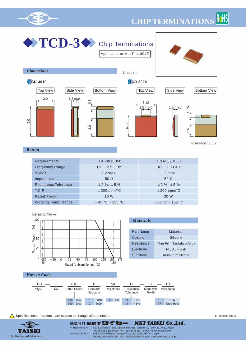
TCD-3
CHIP TERMINATIONS
Unit : mm
Bottom ViewSide ViewTop View0.
63.
0
5.0
1.2 max.3.0
0.75
3.56.
12
2.50.5 1.5 max.6.12
Bottom ViewSide ViewTop View
Tolerance :0.2
TCD-3010 TCD-3020
Rat
ed P
ower
[%
]
100
75
50
25
055
25 0 25 50 75 100 125 150 175155Rated Ambient Temp. [ C]
5050
TCDStyle
3No.
BElectrodeStructure
50 50
50Resistance
010Rated Power
010020
10W20W
GResistanceTolerance
2%5%
GJ
30103020
BC
GMade with
RoHS
TRPackaging
BulkTape Reel
-TR
Derating Curve
e-tcd3xxx-p01-07
http: / /www.mkt- ta isei .co. jp/
Specifications of products are subject to change without notice.
<< Head Office >> 3-10-8, Nohagi 1st Bldg, Minami-Ikebukuro, Toshima-ku, Tokyo, 171-0022, Japan. PHONE : 81-3-3982-0029 FAX : 81-3-3986-1537 E-mail : [email protected]<< Kansai Branch >> 3-18-9, Nishi-Nakajima, Yodogawa-ku, Osaka-City, 532-0011, Japan. PHONE : 81-6-6390-7264 FAX : 81-6-6390-6945 E-mail : [email protected]
Chip Terminations
Dimensions
Rating
Requirements
Frequency Range
VSWR
Impedance
Resistance Tolerance
T.C.R.
Rated Power
Working Temp. Range
TCD-3010B50
DC ~ 2.5 GHz
1.2 max.
50 2 %, 5 %200 ppm/C
10 W
45 C ~ 150 C
TCD-3020C50
DC ~ 2.3 GHz
1.2 max.
50 2 %, 5 %200 ppm/C
20 W
55 C ~ 155 C
Materials
Part Name
Coating
Resistance
Electrode
Substrate
Materials
Silicone
Thin Film Tantalum Alloy
Ni / Au Flash
Aluminum Nitride
Applicable to MIL-R-11804E
How to Code

e-tapereel-p01-05
http: / /www.mkt- ta isei .co. jp/
Specifications of products are subject to change without notice.
<< Head Office >> 3-10-8, Nohagi 1st Bldg, Minami-Ikebukuro, Toshima-ku, Tokyo, 171-0022, Japan. PHONE : 81-3-3982-0029 FAX : 81-3-3986-1537 E-mail : [email protected]<< Kansai Branch >> 3-18-9, Nishi-Nakajima, Yodogawa-ku, Osaka-City, 532-0011, Japan. PHONE : 81-6-6390-7264 FAX : 81-6-6390-6945 E-mail : [email protected]
TAPE & REEL SPECIFICATIONS
Capless and Chip Resistors (TSR)
Unit : mm
Unit : mm
Style
TSR40
TSR45
TSR50S/50
TSR55/60S
TSR60
TSR65
TSR70
A
0.650.1
1.10.2
1.650.2
2.00.2
2.90.1
2.80.1
3.50.1
B
1.150.1
1.90.2
2.40.2
3.60.2
3.50.1
5.30.1
6.750.1
C
8.00.2
12.00.2
D
3.50.05
5.50.05
E
1.750.1
F
4.00.1
G
2.00.05
H
2.00.05
4.00.1
t
1.0 max.
Fig.
Fig.2
Fig.1
Style
TSR40
TSR45
TSR50S/50
TSR55/60S
TSR60
TSR65
TSR70
B
50 min.
C
13
W
13.52.0
TAPE
REEL
t
B
A F HG
ED C
Sproket Hole (1.5 )0.10
Cavity for Components
t
178
C
B
W
B
A F HG
ED C
Sproket Hole (1.5 )0.10
Cavity for Components
Fig. 1 Fig. 2 : TSR40
Available in embossed tape for Capless resistors and paper tape for chip resistors.
Carrier Type
e-tapereel-p02-06Specifications of products are subject to change without notice.
ht tp: / /www.mkt- ta isei .co. jp/
<< Head Office >> 3-10-8, Nohagi 1st Bldg, Minami-Ikebukuro, Toshima-ku, Tokyo, 171-0022, Japan. PHONE : 81-3-3982-0029 FAX : 81-3-3986-1537 E-mail : [email protected]<< Kansai Branch >> 3-18-9, Nishi-Nakajima, Yodogawa-ku, Osaka-City, 532-0011, Japan. PHONE : 81-6-6390-7264 FAX : 81-6-6390-6945 E-mail : [email protected]
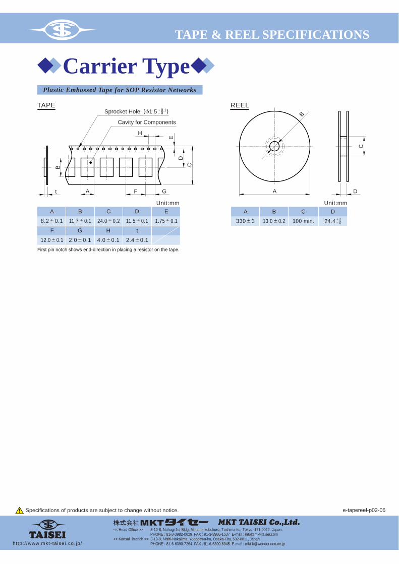
TAPE & REEL SPECIFICATIONS
Plastic Embossed Tape for SOP Resistor Networks
TAPE REEL
A
3303
B
13.00.2
C
100 min.
D
24.42
0
Unit:mmA
8.20.1
G
2.00.1
B
11.70.1
H
4.00.1
C
24.00.2
t
2.40.1
D
11.50.1
E
1.750.1
F
12.00.1
Unit:mm
First pin notch shows end-direction in placing a resistor on the tape.
t
B
A F G
H
E
DC
Sprocket Hole (1.5 )
Cavity for Components
0.10
A D
C
B
Carrier Type

Resistors TAISEIOHM
HEAD OFFICE
KANSAI BRANCH
3-10-8, Nohagi 1st Bldg, Minami-ikebukuro, Toshima-ku, Tokyo, 171-0022, Japan.TEL:81-3-3982-0029 FAX:81-3-3986-1537E-mail : [email protected], Nishi-nakajima, Yodogawa-ku, Osaka-shi, 532-0011, Japan.TEL:81-6-6390-7264 FAX:81-6-6390-6945E-mail : [email protected]
HEAD OFFICE 6972, Shimo-yoshida, Chichibu-shi, Saitama-ken, 369-1593, Japan.TEL:81-494-77-1211 FAX:81-494-77-1415
(BUSINESS)
TAISEI Co.,Ltd.
MKT-TAISEI Co.,Ltd.
URL : http://www.mkt-taisei.co.jp/2014.7 1 6 6