timing closure in 65-nanometer asics using statistical static timing ... · timing closure in...
TRANSCRIPT

© 2009 IBM Corporation
Timing Closure in 65-nanometer ASICs Using Statistical Static Timing Analysis Design Methodology
Llewellyn B. Marshall ([email protected]) Eric A. Foreman ([email protected])

2July, 2009 65 nm Statistical Timing: Marshall/Foreman
Outline
� Statistical Static Timing Analysis (SSTA) Timing Methodology
� Timing Closure Methodology
� Design Experience
� Methodology Usability
� Summary

3July, 2009 65 nm Statistical Timing: Marshall/Foreman
Methodology Modeling
� Silicon / Metal Sources of Variation
� Chip-to-chip variability
� Systematic OCV variability
� Random OCV variability
� Metal layer-to-layer variability
� 14 Process Parameters Used
� Environment, Aging
� N/P Skew, Voltage threshold
� Metal Layer
� Systematic, Random OCV
� RSS (Root Sum Squared) across parameters and along path used for pessimism reduction

4July, 2009 65 nm Statistical Timing: Marshall/Foreman
Variation Modeling
On C
hip
De
lay
Chip-to-Chip VariationBC WCNOM
Max Systematic OCV Range
WC Process
BC Process
Performance advantage
With RSS
5July, 2009 65 nm Statistical Timing: Marshall/Foreman
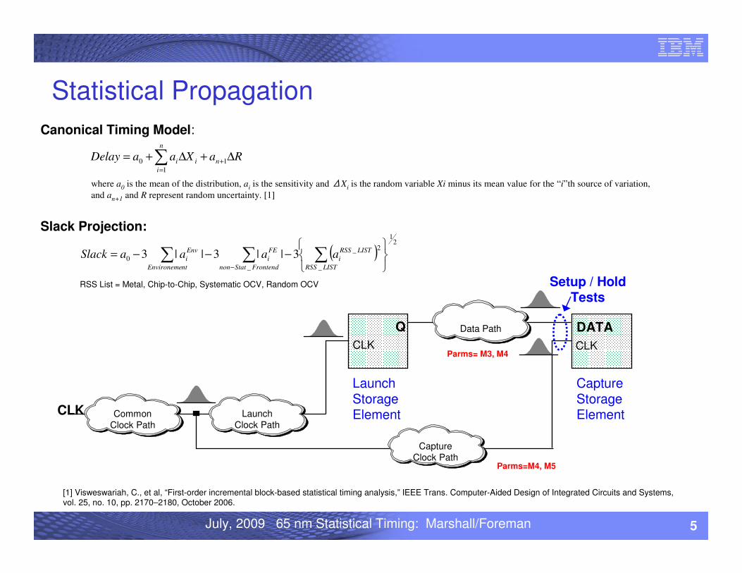
Statistical Propagation
CLK
Q DATA
CLK
Common
Clock Path
Launch
Clock Path
Data Path
Capture
Clock Path
Launch StorageElement
Capture StorageElement
Setup / HoldTests
CLK
Parms=M4, M5
Parms= M3, M4
( )2
1
_
2_
_
0 3||3||3
−−−= ∑∑∑− LISTRSS
LISTRSS
i
FrontendStatnon
FE
i
ntEnvironeme
Env
i aaaaSlack
Canonical Timing Model:
Slack Projection:
RSS List = Metal, Chip-to-Chip, Systematic OCV, Random OCV
∑=
+∆+∆+=
n
i
nii RaXaaDelay1
10
where a0 is the mean of the distribution, ai is the sensitivity and ΔXi is the random variable Xi minus its mean value for the “i”th source of variation,
and an+1 and R represent random uncertainty. [1]
1.[1] Visweswariah, C., et al, “First-order incremental block-based statistical timing analysis,” IEEE Trans. Computer-Aided Design of Integrated Circuits and Systems, vol. 25, no. 10, pp. 2170–2180, October 2006.

6July, 2009 65 nm Statistical Timing: Marshall/Foreman
Timing Methodology
� Statistical Full Process Sign-off � Statistical Static Timing Analysis (SSTA)
� Timing slack quantities projected to worst corner with statistical benefits
� Complete timing sign-off of tests achieved
� Deterministic Timing� Traditional Static Timing Analysis (STA)
� Have ability to perform timing on n-number of specific corners
� Statistical Timing for sub-space� Can project statistical timing to n-number of corners for verification.
� Statistical timing can find n-number of worst corners

7July, 2009 65 nm Statistical Timing: Marshall/Foreman
Timing Closure Flow
ZWL AnalysisIdeal Clocks
Post-layout/opt Ideal Clocks
Post-Clkinsertion
Real Clocks
Wired Real Clocks
Post-ClkOptimized
Real Clocks
Post-Wired Optimized
Real Clocks
Wired Real Clocks+ Coupling
Deterministic Timing
Wired Statistical
Real Clocks+ Coupling
ECO/Opt
Statistical Timing
ECO/Opt
ECO/Opt
ECO/Opt
ECO/Opt
Clk Insert
PDS/Place/Opt
PDS/ReOpt
PDS/ReOpt+EMPAD
Router
Release Design
RAPIDSReOpt
PDS: Timing driven placement and
optimization tool
RAPIDS: Advanced optimization and
routing tool.

8July, 2009 65 nm Statistical Timing: Marshall/Foreman
Timing Closure Environment
� Most timing closure effort spent in STA timing environment
� SSTA runs were employed only after the STA runs were clean
� STA environment specific corners match IBM manufacturing process skew
� STA also included pessimism reduction credits
� STA and SSTA both included Layer-to-Layer metal variation
� Chip sizes have increased dramatically from previous technologies� Some designs now have > 15M placeable objects
� Runtimes and memory footprint can be reduced via a hierarchical methodology
� Divide and conquer (many small pieces in parallel)
� Black box and pruning techniques to reduce top-level run sizes
� SSTA requires ~ 1.5 x the memory footprint and 2.5x cpu (SMP) time as compared to STA

9July, 2009 65 nm Statistical Timing: Marshall/Foreman
Statistical Timing Closure Experience
� Most timing problems were due to:� Clock commonality between launch and capture flops
� Total clock latency
� Careful attention must be given to clock composition and structure � Logic gate types should be chosen to minimize latency while providing a statistically stable result
� Common wire levels and VT libraries should be used throughout the clock tree
� Many more HOLD issues seen in WC process than in previous technologies. � This occurs if the clock skew variability approaches the CLK->Q delay of the base flops
� Hierarchical paths can be problematic due to the inherent clock non-commonality� Hierarchy should be latch bounded
� Many of the SSTA failures were difficult STA paths that became more critical
� Cross talk induced coupling delay with process variation was a common source of fails
� Most SSTA failures were corrected via traditional means
10July, 2009 65 nm Statistical Timing: Marshall/Foreman
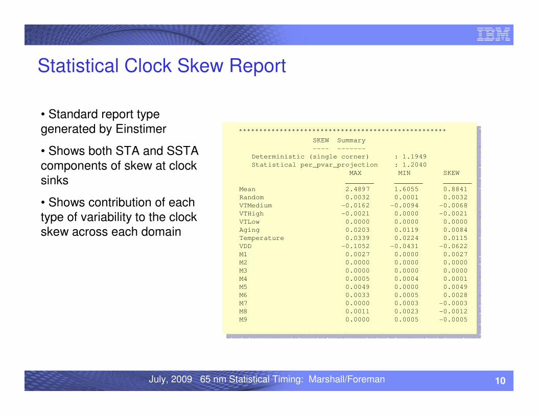
***************************************************
SKEW Summary
---- -------
Deterministic (single corner) : 1.1949
Statistical per_pvar_projection : 1.2040
MAX MIN SKEW
_______ _______ _______
Mean 2.4897 1.6055 0.8841
Random 0.0032 0.0001 0.0032
VTMedium -0.0162 -0.0094 -0.0068
VTHigh -0.0021 0.0000 -0.0021
VTLow 0.0000 0.0000 0.0000
Aging 0.0203 0.0119 0.0084
Temperature 0.0339 0.0224 0.0115
VDD -0.1052 -0.0431 -0.0622
M1 0.0027 0.0000 0.0027
M2 0.0000 0.0000 0.0000
M3 0.0000 0.0000 0.0000
M4 0.0005 0.0004 0.0001
M5 0.0049 0.0000 0.0049
M6 0.0033 0.0005 0.0028
M7 0.0000 0.0003 -0.0003
M8 0.0011 0.0023 -0.0012
M9 0.0000 0.0005 -0.0005
Statistical Clock Skew Report
• Standard report type
generated by Einstimer
• Shows both STA and SSTA
components of skew at clock sinks
• Shows contribution of each
type of variability to the clock skew across each domain

11July, 2009 65 nm Statistical Timing: Marshall/Foreman
***************************************************Flop/Data
Hold Flop/Clk
Can. Model ( slack = data AT - guard – clk AT - clk adj )
Mean ( 0.192 : 101.862 - 0.026 - 101.643 - -0.000 )
RandomOCV 0.000 0.000 0.000 0.000 0.000
SysOCV -0.057 -0.037 0.000 0.020 0.000
SiProcess -0.012 -0.146 -0.003 -0.131 0.000
NPskew 0.005 -0.002 -0.002 -0.005 0.000
Aging -0.000 0.002 0.000 0.002 0.000
Temperature 0.004 0.012 0.000 0.007 0.000
M1 0.002 0.004 0.000 0.002 0.000
M2 0.000 0.001 0.000 0.000 0.000
M3 0.001 0.001 -0.000 -0.000 0.000
M4 0.000 0.000 0.000 0.000 0.000
M5 0.000 0.000 -0.000 0.000 0.000
M6 -0.001 0.000 0.000 0.001 0.000
M7 0.000 0.000 0.000 0.000 0.000
M8 -0.000 0.001 0.000 0.001 0.000
M9 -0.000 0.000 0.000 0.000 0.000
PinName E Phase AT Adj Slack Slew CL pinCL FO Cell NetName
-----------------------------------------------------------------------------------------
Gate6/Z F CLK@L 101.362 0.000w -0.003 0.014 0.002 0.001 1 BUFFER Net12
Gate6/A F CLK@L 101.335 0.027 -0.003 0.016 0.003 0.001 1 BUFFER Net11
Gate5/Z F CLK@L 101.335 0.000w -0.003 0.016 0.003 0.001 1 BUFFER Net10
Gate5/A F CLK@L 101.307 0.027 -0.003 0.014 0.002 0.001 1 BUFFER Net9
Gate4/Z F CLK@L 101.307 0.000w -0.003 0.014 0.002 0.001 1 BUFFER Net8
Gate4/A F CLK@L 101.280 0.026 -0.003 0.015 0.002 0.001 1 BUFFER Net7
Gate3/Z F CLK@L 101.280 0.000w -0.003 0.015 0.002 0.001 1 BUFFER Net6
Gate3/A F CLK@L 101.253 0.026 -0.003 0.013 0.001 0.001 1 BUFFER Net5
Gate2/Z F CLK@L 101.253 0.000w -0.003 0.013 0.001 0.001 1 BUFFER Net4
Gate2/A F CLK@L 101.227 0.026 -0.003 0.016 0.002 0.001 1 BUFFER Net3
Gate1/Z F CLK@L 101.227 0.000w -0.003 0.016 0.002 0.001 1 BUFFER Net2
Gate1/A F CLK@L 101.184 0.041 -0.003 0.068 0.010 0.001 1 BUFFER Net1
-----------------------------------------------------------------------------------------
Statistical Timing Slack Report
• Standard report type
generated by EinsTimer
• Shows both STA and SSTA
components along the test path
• Shows contribution of each
type of variability
• Slack equation displays
method of calculation and mean
values used
12July, 2009 65 nm Statistical Timing: Marshall/Foreman
Summary
� In 2008 IBM introduced SSTA signoff flow for 65 nm ASIC technology
� The timing methodology provided timing coverage across the entire process and environmental space with a limited number of runs
� Traditional STA was used during the early timing closure phase to reduce
runtimes and memory
� SSTA was used primarily for the final sign-off phase
� SSTA variability can be used to identify problems in clock design
� Experience showed that most violations (99.98%) were corrected with STA
� SSTA revealed ~ 0.02% new violations ( ~400 fails out of 5M tests)
� Most SSTA violations were due to clock commonality problems between launch
and capture flops
� Many 65nm designs were released in 2008 using this methodology which has proven to produce working hardware at predictable yields