behavioral modeling methods for switched-capacitor Σ∆ modulators
TRANSCRIPT

352 IEEE TRANSACTIONS ON CIRCUITS AND SYSTEMS—I: FUNDAMENTAL THEORY AND APPLICATIONS, VOL. 50, NO. 3, MARCH 2003
Behavioral Modeling of Switched-CapacitorSigma–Delta Modulators
Piero Malcovati, Member, IEEE, Simona Brigati, Member, IEEE, Fabrizio Francesconi, Member, IEEE,Franco Maloberti, Fellow, IEEE, Paolo Cusinato, and Andrea Baschirotto, Senior Member, IEEE
Abstract—This paper presents a complete set of blocks imple-mented in the popular MATLAB SIMULINK environment, whichallows designers to perform time-domain behavioral simulationsof switched-capacitor (SC) sigma–delta(��) modulators. Theproposed set of blocks takes into account most of the SC��modulator nonidealities, such as sampling jitter, noise,and operational amplifier parameters (white noise, finite dc gain,finite bandwidth, slew rate and saturation voltages). For eachblock, a description of the considered effect as well as all of theimplementative details are provided. The proposed simulationenvironment is validated by comparing the simulated behaviorwith the experimental results obtained from two actual circuits,namely a second-order low-pass and a sixth-order bandpass SC�� modulator.
Index Terms—Analog–digital conversion, discrete-time systems,sigma–delta(��) modulation.
I. INTRODUCTION
SIGMA–DELTA modulators are the most suitableA/D converter topologies for digitizing with high-res-
olution analog signals characterized by a bandwidth (BW)much smaller than the sampling frequency . With thesearchitectures, a resolution up to 19–21 bits can be reachedusing standard IC technologies [2]–[4]. These features makethe solutions very attractive for a number of applications.For instance, they have gained increasing popularity in audioapplications (where a low-pass signal BW requires a resolutionup to 20 bit), in receivers for communication systems (wherethe modulated signal can be digitized at the interface with abandpass modulator), in sensor interface circuits and inmeasurement systems. Key advantages ofmodulators aretheir inherent linearity and their robust analog implementation.Moreover, by trading accuracy with speed, modulatorsallow high performance to be achieved with low sensitivityto analog component imperfections and without requiringcomponent trimming.
Manuscript received February 5, 2002; revised October 16, 2002. This paperwas recommended by Associate Editor O. Feely.
P. Malcovati is with the Department of Electrical Engineering, University ofPavia, 27100 Pavia, Italy (e-mail: [email protected]).
S. Brigati and F. Francesconi are with ACCO Microelettronica S.r.l., 27100Pavia, Italy (e-mail: [email protected]; [email protected]).
F. Maloberti is with the Department of Electronics, University of Pavia, 27100Pavia, Italy (e-mail: [email protected]).
P. Cusinato is with the Texas Instruments France, 06270 Villeneuve Loubet,France (e-mail: [email protected]).
A. Baschirotto is with the Department of Innovation Engineering, Universityof Lecce, 73100 Lecce, Italy (e-mail: [email protected]).
Digital Object Identifier 10.1109/TCSI.2003.808892
modulators can be implemented either with contin-uous-time or with sampled-data techniques. The most popularapproach is based on a sampled-data solution with switched-capacitor (SC) implementation. In fact, SC modulatorscan be efficiently realized in standard CMOS technologyand included in complete mixed-signal systems without anyperformance degradation. For this reason, we will focus on thecase of SC modulators in this paper.
In the design of a high-performance SC modulator, twomain issues have to be addressed by the designers.
1) Which is the best architecture to fulfill the applicationrequirements?
2) For a given architecture, which are the requirements forthe building blocks?
In practice, a significant problem in the design ofmodulators is the estimation of their performance, sincethey are mixed-signal nonlinear circuits. Due to the inherentnonlinearity of the modulator loop the optimization of theperformance has to be carried out with behavioral time-domainsimulations. This situation is quite difficult to handle whena high-performance system is considered. Indeed, to satisfyhigh-performance requirements, accurate simulations of anumber of nonidealities and, eventually, the comparison of theperformance of different architectures are needed in order tochoose the best solution. In addition to this, in the design ofhigh-resolution SC modulators, a large set of parameters,including the performance of the building blocks embedded inthe adopted structure, has to be optimized in order to achievethe desired signal-to-noise ratio (SNR) or signal-to-noise anddistortion ratio (SNDR).1
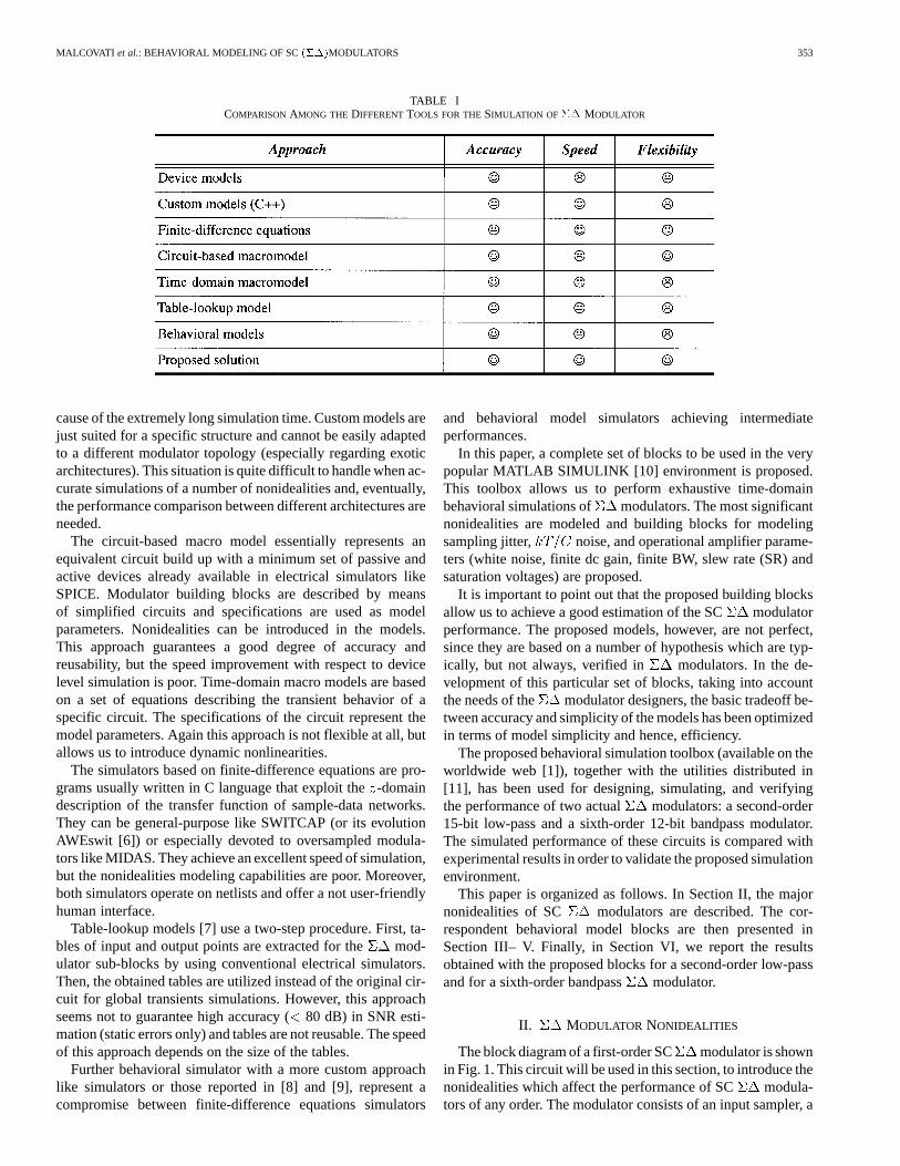
In principle, various approaches for transient simulationwhich include device models (such as SPICE), finite-differenceequations (such as SWITCAP), custom numerical models(typically in C language), etc., are already available.However, in different measures, all of them exhibit somedisadvantages. Table I [5] classifies the different tools in termsof three main characteristics: accuracy, speed, and flexibility(intended as modeling capability plus reusability). Moreover,the post-processing algorithms for the evaluation of modulatorperformances are other qualifying features for the various tools.
SPICE is a conventional electrical simulator and, despite itsprecision, it is not suitable for the analysis of modulators be-
1Notice that the two issues mentioned above are strictly correlated becausearchitectures which achieve optimal results with ideal block models are not nec-essarily the best solution in the presence of building blocks with degraded per-formances. Therefore, the choice of the architecture and design of the buildingblocks require typically concurrent optimization processes.
1057-7122/03$17.00 © 2003 IEEE
MALCOVATI et al.: BEHAVIORAL MODELING OF SC MODULATORS 353
TABLE ICOMPARISONAMONG THE DIFFERENTTOOLS FOR THESIMULATION OF �� MODULATOR
cause of the extremely long simulation time. Custom models arejust suited for a specific structure and cannot be easily adaptedto a different modulator topology (especially regarding exoticarchitectures). This situation is quite difficult to handle when ac-curate simulations of a number of nonidealities and, eventually,the performance comparison between different architectures areneeded.
The circuit-based macro model essentially represents anequivalent circuit build up with a minimum set of passive andactive devices already available in electrical simulators likeSPICE. Modulator building blocks are described by meansof simplified circuits and specifications are used as modelparameters. Nonidealities can be introduced in the models.This approach guarantees a good degree of accuracy andreusability, but the speed improvement with respect to devicelevel simulation is poor. Time-domain macro models are basedon a set of equations describing the transient behavior of aspecific circuit. The specifications of the circuit represent themodel parameters. Again this approach is not flexible at all, butallows us to introduce dynamic nonlinearities.
The simulators based on finite-difference equations are pro-grams usually written in C language that exploit the-domaindescription of the transfer function of sample-data networks.They can be general-purpose like SWITCAP (or its evolutionAWEswit [6]) or especially devoted to oversampled modula-tors like MIDAS. They achieve an excellent speed of simulation,but the nonidealities modeling capabilities are poor. Moreover,both simulators operate on netlists and offer a not user-friendlyhuman interface.
Table-lookup models [7] use a two-step procedure. First, ta-bles of input and output points are extracted for the mod-ulator sub-blocks by using conventional electrical simulators.Then, the obtained tables are utilized instead of the original cir-cuit for global transients simulations. However, this approachseems not to guarantee high accuracy (80 dB) in SNR esti-mation (static errors only) and tables are not reusable. The speedof this approach depends on the size of the tables.
Further behavioral simulator with a more custom approachlike simulators or those reported in [8] and [9], represent acompromise between finite-difference equations simulators
and behavioral model simulators achieving intermediateperformances.
In this paper, a complete set of blocks to be used in the verypopular MATLAB SIMULINK [10] environment is proposed.This toolbox allows us to perform exhaustive time-domainbehavioral simulations of modulators. The most significantnonidealities are modeled and building blocks for modelingsampling jitter, noise, and operational amplifier parame-ters (white noise, finite dc gain, finite BW, slew rate (SR) andsaturation voltages) are proposed.
It is important to point out that the proposed building blocksallow us to achieve a good estimation of the SC modulatorperformance. The proposed models, however, are not perfect,since they are based on a number of hypothesis which are typ-ically, but not always, verified in modulators. In the de-velopment of this particular set of blocks, taking into accountthe needs of the modulator designers, the basic tradeoff be-tween accuracy and simplicity of the models has been optimizedin terms of model simplicity and hence, efficiency.
The proposed behavioral simulation toolbox (available on theworldwide web [1]), together with the utilities distributed in[11], has been used for designing, simulating, and verifyingthe performance of two actual modulators: a second-order15-bit low-pass and a sixth-order 12-bit bandpass modulator.The simulated performance of these circuits is compared withexperimental results in order to validate the proposed simulationenvironment.
This paper is organized as follows. In Section II, the majornonidealities of SC modulators are described. The cor-respondent behavioral model blocks are then presented inSection III– V. Finally, in Section VI, we report the resultsobtained with the proposed blocks for a second-order low-passand for a sixth-order bandpass modulator.
II. MODULATOR NONIDEALITIES
The block diagram of a first-order SC modulator is shownin Fig. 1. This circuit will be used in this section, to introduce thenonidealities which affect the performance of SC modula-tors of any order. The modulator consists of an input sampler, a

354 IEEE TRANSACTIONS ON CIRCUITS AND SYSTEMS—I: FUNDAMENTAL THEORY AND APPLICATIONS, VOL. 50, NO. 3, MARCH 2003
Fig. 1. Schematic of an SC first-order�� modulator.
SC integrator, a quantizer and a feedback digital-to-analog con-verter (DAC). The main nonidealities of this circuit which areconsidered in this paper are the following:
1) clock jitter at the input sampler;2) switch thermal noise in the SC structure;3) operational amplifier noise;4) operational amplifier finite gain;5) operational amplifier BW;6) operational amplifier SR;7) operational amplifier saturation voltages.
The use of the SC technique for the implementation meansthat all the blocks in a SC modulator are properly synchro-nized. Using the building blocks presented in the following sec-tions, the simulation of any SC modulator is possible.
The basic concept of the proposed simulation environmentis the evaluation of the output samples in the time domain. Thenonidealities listed above produce a deviation of the output sam-ples from their ideal values. The overall performance of the
modulator is then evaluated in the frequency domain afterproper fast Fourier transform (FFT) [12] of the output samples(see the Appendix).
III. CLOCK JITTER
The operation of an SC circuit depends on complete chargetransfers during each of the clock phases [13]. Once the analogsignal has been sampled, the SC circuit is a sampled-data systemwhere variations of the clock period have no direct effect on thecircuit performance. Therefore, the effect of clock jitter on anSC circuit is completely described by computing its effect onthe sampling of the input signal. This also means that the effectof clock jitter on a modulator is independent of the structureor order of the modulator.
Clock jitter results in a nonuniform sampling time sequence,and produces an error which increases the total error power atthe quantizer output. The magnitude of this error is a functionof both the statistical properties of the jitter and the modulatorinput signal. The error introduced when a sinusoidal signalwith amplitude and frequency is sampled at an instantwhich is in error by an amount is given by
(1)
Fig. 2. Modeling a random sampling jitter.
Fig. 3. Model of a “noisy” integrator.
This effect can be simulated at behavioral level by using themodel shown in Fig. 2, which implements (1). The input signal
and its derivative are continuous-time signals.They are sampled with sampling period by a zero-orderhold. In the model, we assumed that the sampling uncertainty
is a Gaussian random process with standard deviation. The signal is implemented starting from a sequence
of random numbers with Gaussian distribution, zero mean,and unity standard deviation (available in SIMULINK). Otherpossible distributions can be considered and consequentlyimplemented in this block. Whether oversampling is helpful inreducing the error introduced by the jitter depends on the natureof the jitter. Since we assume the jitter white, the resultant errorhas uniform power-spectral density (PSD) from 0 to , witha total power of . In this case, the total errorpower will be reduced by the oversampling ratio [14].
IV. THERMAL AND OPERATIONAL AMPLIFIER NOISE
The most important noise sources affecting the operation ofan SC modulator are the thermal noise associated to thesampling switches and the intrinsic noise of the operationalamplifiers.
These effects can be successfully simulated at the behaviorallevel by using the model of a “noisy” integrator shown in Fig. 3,which represents the SC integrator shown in Fig. 1 (a similarmodel can be used also for resonators). The-domain transferfunction of this integrator is given by
(2)

MALCOVATI et al.: BEHAVIORAL MODELING OF SC MODULATORS 355
Fig. 4. Modeling switches thermal noise (kT=C block).
where the variable represents the coefficient of theintegrator. The input signal is multiplied by in theblock.
Each noise source and its relevant model will be described inthe following paragraphs.
A. Switches Thermal Noise
Thermal noise is caused by the random fluctuation of car-riers due to thermal energy and is present even at equilibrium.Thermal noise has a white spectrum and wide band, limited onlyby the time constant of the switched capacitors or the BW ofthe operational amplifiers. Referring to the SC first-ordermodulator shown in Fig. 1, the sampling capacitoris in se-ries with a switch, with finite resistance , that periodicallyopens, thus sampling a noise voltage onto. The total noisepower can be found evaluating the integral [5]
(3)
where is the Boltzmann’s constant, the absolute temper-ature, and the noise PSD associated with the switchon-resistance. The switch thermal noise voltage(usuallycalled noise) is then superimposed to the input voltage
leading to
(4)
where denotes a Gaussian random process with unity stan-dard deviation, while is the coefficient of the in-tegrator. Equation (4) is implemented by the model shown inFig. 4.
The integrators or resonators of an SC modulator mayinclude more than one SC input branch, each contributing tothe total noise power. For example, in the modulator shownin Fig. 1, there are two input branches, one carrying the signaland the other providing the feedback from the modulator output.Each branch has to be modeled with a separate noiseblock, including the proper coefficient(different coefficientscan be used in the different branches).
Fig. 5. Operational amplifier noise model (OpNoise block).
Fig. 6. Real integrator model.
B. Operational Amplifier Noise
Fig. 5 shows the model used to simulate the effect of theoperational amplifier noise [15]. Here, represents the total
noise voltage of the operational amplifier referred to theintegrator (or resonator) input. In this model we consideredonly thermal noise, while flicker noise and dc offset areneglected. Indeed, in low-pass modulators, flicker noiseand dc offset are typically canceled by means of auto-zero, cor-related double sampling, or chopper stabilization techniques,while they are not important in bandpass architectures. Thenoise power can be evaluated through a transistor-levelnoise simulation of the complete integrator in the proper clockphase, including feedback, sampling and load capacitors (clockphase in Fig. 1). The resulting output referred noise PSD hasto be integrated over the whole frequency spectrum, eventuallytaking into account the degradation of the thermal noise PSDintroduced by the auto-zero or correlated double samplingtechniques [16], and then divided by in order to refer theobtained noise power to the integrator input.
In this model, we consider only the contribution of the sam-pled noise, assuming that no continuous-time paths are presentacross the modulator (this is typically the case in SCmodulators due to the presence of a latched quantizer).
V. OPERATIONAL AMPLIFIER NONIDEALITIES
The behavioral model of an ideal integrator with unity coef-ficient is shown in the inset of Fig. 3. Its transfer function is
(5)
Analog circuit implementations of the integrator or resonatordeviate from this ideal behavior due to several nonideal effects.One of the major causes of performance degradation in SCmodulators is the incomplete transfer of charge in the SC inte-grators. This nonideal effect is a consequence of the operationalamplifier nonidealities, namely finite gain and BW, SR, and sat-uration voltages [17]. These will be considered separately in thefollowing sections. Fig. 6 shows the model of the real integratorincluding all the nonidealities. A similar model, based on thesame building blocks can also be realized for real resonators.
356 IEEE TRANSACTIONS ON CIRCUITS AND SYSTEMS—I: FUNDAMENTAL THEORY AND APPLICATIONS, VOL. 50, NO. 3, MARCH 2003
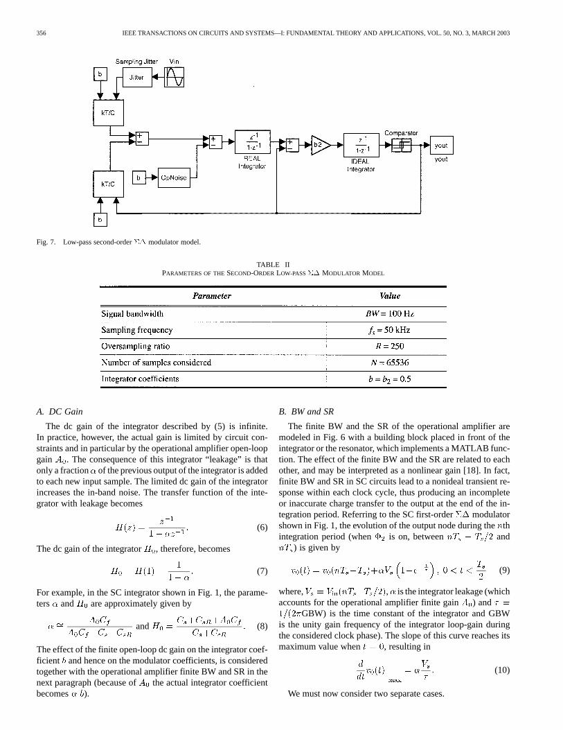
Fig. 7. Low-pass second-order�� modulator model.
TABLE IIPARAMETERS OF THESECOND-ORDER LOW-PASS�� MODULATOR MODEL
A. DC Gain
The dc gain of the integrator described by (5) is infinite.In practice, however, the actual gain is limited by circuit con-straints and in particular by the operational amplifier open-loopgain . The consequence of this integrator “leakage” is thatonly a fraction of the previous output of the integrator is addedto each new input sample. The limited dc gain of the integratorincreases the in-band noise. The transfer function of the inte-grator with leakage becomes
(6)
The dc gain of the integrator , therefore, becomes
(7)
For example, in the SC integrator shown in Fig. 1, the parame-ters and are approximately given by
and (8)
The effect of the finite open-loop dc gain on the integrator coef-ficient and hence on the modulator coefficients, is consideredtogether with the operational amplifier finite BW and SR in thenext paragraph (because of the actual integrator coefficientbecomes ).
B. BW and SR
The finite BW and the SR of the operational amplifier aremodeled in Fig. 6 with a building block placed in front of theintegrator or the resonator, which implements a MATLAB func-tion. The effect of the finite BW and the SR are related to eachother, and may be interpreted as a nonlinear gain [18]. In fact,finite BW and SR in SC circuits lead to a nonideal transient re-sponse within each clock cycle, thus producing an incompleteor inaccurate charge transfer to the output at the end of the in-tegration period. Referring to the SC first-order modulatorshown in Fig. 1, the evolution of the output node during thethintegration period (when is on, between and
) is given by
(9)
where, , is the integrator leakage (whichaccounts for the operational amplifier finite gain) and
GBW) is the time constant of the integrator and GBWis the unity gain frequency of the integrator loop-gain duringthe considered clock phase). The slope of this curve reaches itsmaximum value when , resulting in
(10)
We must now consider two separate cases.
MALCOVATI et al.: BEHAVIORAL MODELING OF SC MODULATORS 357
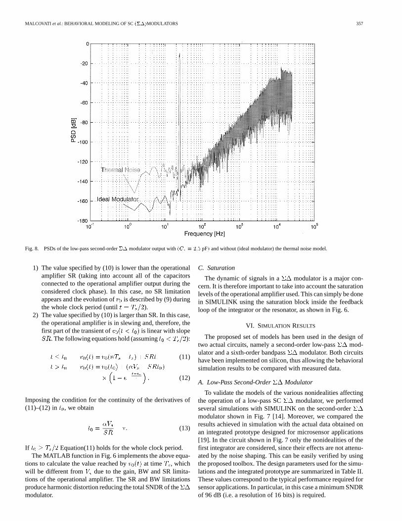
Fig. 8. PSDs of the low-pass second-order�� modulator output with(C = 2:5 pF) and without (ideal modulator) the thermal noise model.
1) The value specified by (10) is lower than the operationalamplifier SR (taking into account all of the capacitorsconnected to the operational amplifier output during theconsidered clock phase). In this case, no SR limitationappears and the evolution of is described by (9) duringthe whole clock period (until ).
2) The value specified by (10) is larger than SR. In this case,the operational amplifier is in slewing and, therefore, thefirst part of the transient of is linear with slope
. The following equations hold (assuming ):
(11)
(12)
Imposing the condition for the continuity of the derivatives of(11)–(12) in , we obtain
(13)
If Equation(11) holds for the whole clock period.The MATLAB function in Fig. 6 implements the above equa-
tions to calculate the value reached by at time , whichwill be different from due to the gain, BW and SR limita-tions of the operational amplifier. The SR and BW limitationsproduce harmonic distortion reducing the total SNDR of themodulator.
C. Saturation
The dynamic of signals in a modulator is a major con-cern. It is therefore important to take into account the saturationlevels of the operational amplifier used. This can simply be donein SIMULINK using the saturation block inside the feedbackloop of the integrator or the resonator, as shown in Fig. 6.
VI. SIMULATION RESULTS
The proposed set of models has been used in the design oftwo actual circuits, namely a second-order low-pass mod-ulator and a sixth-order bandpass modulator. Both circuitshave been implemented on silicon, thus allowing the behavioralsimulation results to be compared with measured data.
A. Low-Pass Second-Order Modulator
To validate the models of the various nonidealities affectingthe operation of a low-pass SC modulator, we performedseveral simulations with SIMULINK on the second-ordermodulator shown in Fig. 7 [14]. Moreover, we compared theresults achieved in simulation with the actual data obtained onan integrated prototype designed for microsensor applications[19]. In the circuit shown in Fig. 7 only the nonidealities of thefirst integrator are considered, since their effects are not attenu-ated by the noise shaping. This can be easily verified by usingthe proposed toolbox. The design parameters used for the simu-lations and the integrated prototype are summarized in Table II.These values correspond to the typical performance required forsensor applications. In particular, in this case a minimum SNDRof 96 dB (i.e. a resolution of 16 bits) is required.

358 IEEE TRANSACTIONS ON CIRCUITS AND SYSTEMS—I: FUNDAMENTAL THEORY AND APPLICATIONS, VOL. 50, NO. 3, MARCH 2003
Fig. 9. PSDs of the low-pass second-order�� modulator output with (SR = 0:1 V=�s and GBW= 100 kHz) and without (ideal modulator) the operationalamplifier finite-BW and SR model.
Fig. 10. SNDR of the low-pass second-order�� modulator as a function of the input signal amplitude for different values of the operational amplifier saturationvoltage(V ).
Fig. 8 shows the PSDs of the modulator output bitstreamobtained in simulation without (ideal modulator) and with
the thermal noise model. The value of the sam-pling capacitance used in the simulation is 2.5 pF. The

MALCOVATI et al.: BEHAVIORAL MODELING OF SC MODULATORS 359
TABLE IIISNDRAND RESOLUTION OFSECOND–ORDER LOW-PASS�� MODULATOR
Fig. 11. Noise PSDs of the low-pass second-order�� modulator resulting from simulation (considering all of the nonidealities) and measurements.
noise produces a noise floor at low frequencies, asexpected.
Likewise, Fig. 9 shows the PSDs of the modulator outputobtained in simulation without (ideal modulator) and with theoperational amplifier finite BW and SR model. The SR and BW(GBW) values used in the simulation are 0.1 Vs and 100 kHz,respectively. The finite BW and SR lead to harmonic distortion,thus degrading the SNDR performance of the modulator.
The effect of the operational amplifier saturation voltageon the performance of the modulator is illustrated
in Fig. 10, by plotting the simulated SNDR as a function ofthe input signal amplitude for different values of . Theideal modulator operates properly up to a signal amplitudeof 6 dB, with respect to the reference voltage. A saturationvoltage V with a reference voltage of 1 Vdoes not degrade the performance significantly, while for
V a significant degradation occurs for signalamplitudes larger than 13 dB, since, due to the saturation ofthe operational amplifiers, the modulator loop cannot followthe input signal.
360 IEEE TRANSACTIONS ON CIRCUITS AND SYSTEMS—I: FUNDAMENTAL THEORY AND APPLICATIONS, VOL. 50, NO. 3, MARCH 2003
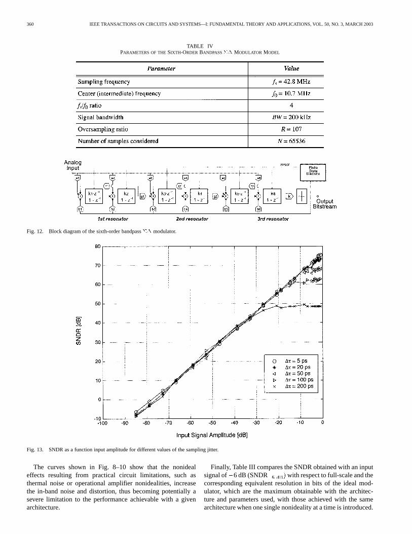
TABLE IVPARAMETERS OF THESIXTH-ORDER BANDPASS�� MODULATOR MODEL
Fig. 12. Block diagram of the sixth-order bandpass�� modulator.
Fig. 13. SNDR as a function input amplitude for different values of the sampling jitter.
The curves shown in Fig. 8–10 show that the nonidealeffects resulting from practical circuit limitations, such asthermal noise or operational amplifier nonidealities, increasethe in-band noise and distortion, thus becoming potentially asevere limitation to the performance achievable with a givenarchitecture.
Finally, Table III compares the SNDR obtained with an inputsignal of 6 dB (SNDR with respect to full-scale and thecorresponding equivalent resolution in bits of the ideal mod-ulator, which are the maximum obtainable with the architec-ture and parameters used, with those achieved with the samearchitecture when one single nonideality at a time is introduced.

MALCOVATI et al.: BEHAVIORAL MODELING OF SC MODULATORS 361
Fig. 14. PSDs of the bandpass sixth-order�� modulator output showing the effect of the operational amplifier finite BW (GBW= 150 MHz).
TABLE VDESIGN PARAMETERS USED FOR THESIXTH-ORDER BANDPASS�� MODULATOR SIMULATION
Moreover, the overall (SNDR achieved in simulation con-sidering all of the nonidealities is compared with the measureddata obtained on the integrated prototype, fabricated using adouble-poly, double-metal 2-m CMOS technology. The valuesof the parameters used in the simulations correspond to the de-sign parameters of the chip. Fig. 11 compares the noise PSDobtained in simulation considering all of the nonidealities withthe noise PSD resulting from the measured data.
B. Bandpass Sixth-Order Modulator
To validate the models of the various nonidealities affectingthe operation of a SC bandpass modulator, we performedseveral simulations with SIMULINK on the sixth-order modu-lator shown in Fig. 12 [20], [21]. In this model, the nonidealitiesof all the integrators were considered. The features of the band-pass modulator and the simulation parameters are reported inTable IV.
Bandpass modulators are more sensitive to samplingjitter than low-pass ones [13]. Fig. 13 shows the simulatedSNDR as a function of the input amplitude for different valuesof the sampling jitter . The limitation due to the jitterappears mainly in a limitation of the SNDR peak and not in thedynamic range (DR).
Fig. 14 shows the effect of an operational amplifier finite BW(GBW MHz) on the output PSD of the SC bandpassmodulator. In this case, the operational amplifier nonidealitiesproduce a shift of the notch frequencies in the bandpass noisetransfer function. However, the application requirements (andhence the decimating filter center frequency) are restricted to agiven BW and therefore the shift of the notch frequencies resultsin an increase of the in-band quantization noise.
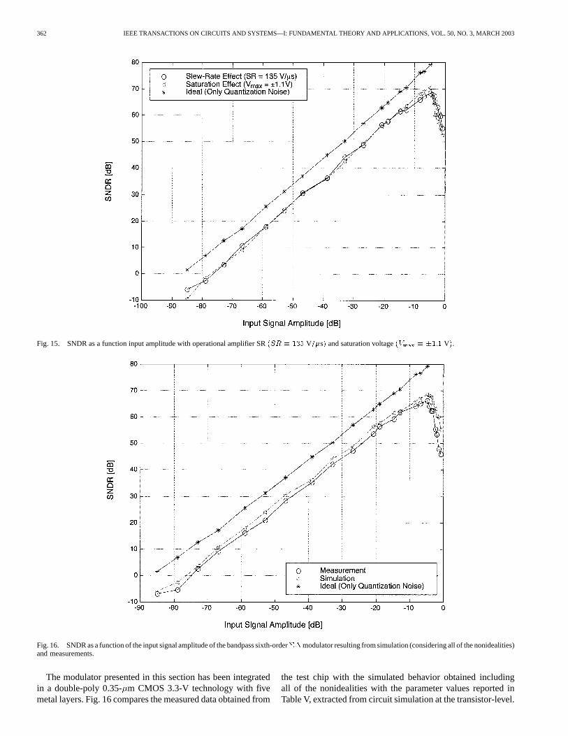
Fig. 15 shows the SNDR as a function of the input signalamplitude when an SR (positive and negative) of 135 Vs andsaturation voltages of 1.1 V are used. The effect of both thesenonidealities is a degradation of the SNDR for large input signalamplitude, due to the saturation of the modulator loop.
362 IEEE TRANSACTIONS ON CIRCUITS AND SYSTEMS—I: FUNDAMENTAL THEORY AND APPLICATIONS, VOL. 50, NO. 3, MARCH 2003
Fig. 15. SNDR as a function input amplitude with operational amplifier SR(SR = 135 V=�s) and saturation voltage(V = �1:1 V).
Fig. 16. SNDR as a function of the input signal amplitude of the bandpass sixth-order��modulator resulting from simulation (considering all of the nonidealities)and measurements.
The modulator presented in this section has been integratedin a double-poly 0.35-m CMOS 3.3-V technology with fivemetal layers. Fig. 16 compares the measured data obtained from
the test chip with the simulated behavior obtained includingall of the nonidealities with the parameter values reported inTable V, extracted from circuit simulation at the transistor-level.

MALCOVATI et al.: BEHAVIORAL MODELING OF SC MODULATORS 363
The measured SNDR as a function of the input signal amplitudeis in good agreement with the results of the behavioral simu-lations. By comparing Fig. 15 and Fig. 16, it appears that op-erational amplifier SR and saturation are the dominant effectswhich affect the performance of the modulator.
VII. CONCLUSION
In this paper, we presented a set of models implemented in thepopular MATLAB SIMULINK environment suitable for time-domain behavioral simulations of SC modulators. The pro-posed set of models takes into account at the behavioral levelmost of the SC modulator nonidealities, such as samplingjitter, noise, and operational amplifier parameters (whitenoise, finite dc-gain, finite BW, SR and saturation voltages),thus allowing us to obtain a good estimation of the mod-ulator performance with a short simulation time (about 4096simulated samples per second on the second-ordermod-ulator, including post-processing of the output data). The pro-posed simulation environment has been validated by comparingthe simulated behavior with the experimental results obtainedfrom both a second-order low-pass and a sixth-order bandpass
modulator. The proposed set of models will be expanded inthe future to include additional nonidealities, such as the non-linearity of the sampling switches and of the D/A converter.
APPENDIX
The SNR and the SNDR of a modulator are defined as
SNR and SNDR (14)
respectively, where denotes the signal power, the noisepower, and the power of the harmonics of the signal. In anideal modulator, the SNR is determined only by the quan-tization noise according to
SNR (15)
where denotes the input range of the modulator, thenumber of bits in the quantizer, the oversampling ratio, and
the order of the modulator.However, the other noise or distortion sources increase the
total noise power of the data converter above the quantizationnoise level and contribute to both the SNR and the SNDR.
The calculation of the SNR or SNDR of a modulatorstarting from the raw output data (output samples) is performedin two steps. In the first step, the sinusoidal signal is ex-tracted from the sequence of output data ( , at time ),typically by computing a discrete Fourier transform (DFT) of
at the signal frequency
(16)
where denotes the desired window for the data (typicallythe Hanning window). The obtained signal is then subtractedfrom the raw output signal in the time domain, thus obtaining asignal which contains only the noise and distortion con-tributions. In the second step, we calculate the FFT ofand of
, obtaining the spectra of the signal and ofthe noise . The same window used for the DFT hasto be used also for the FFT. Finally, the signal and noise
power are calculated by integrating the power spectra
and (17)
where denotes the number of samples cor-responding to the desired BW (baseband, BW) with samplingfrequency . The SNR (or SNDR) is then obtained from (14).
REFERENCES
[1] Category: Control Systems, File: SD Toolbox [Online]. Available:http://www.mathworks.com/matlabcentral/fileexchange
[2] B. P. Del Signore, D. A. Kerth, N. S. Sooch, and E. J. Swanson, “Amonolithic 20-b delta-sigma A/D converter,”IEEE J. Solid-State Cir-cuits, vol. 25, pp. 1311–1317, Dec. 1990.
[3] D. A. Kerth, D. B. Kasha, T. G. Melissinos, D. S. Piasecki, and E. J.Swanson, “A 120 dB linear switched-capacitor delta-sigma modulator,”in Proc. IEEE Int. Solid-State Circuit Conf. (ISSCC ’94), San Francisco,CA, 1994, pp. 196–197.
[4] O. Nys and R. K. Anderson, “A 19-bit low-power multibit sigma–deltaADC based on data weighted averaging,”IEEE J. Solid-State Circuits,vol. 32, pp. 933–942, July 1997.
[5] S. R. Norsworthy, R. Schreier, and G. C. Temes, “Delta-sigma dataconverters,” inTheory, Design and Simulation. Piscataway, NJ: IEEEPress, 1997.
[6] R. Trihy and R. Rohrer, “A switched capacitor circuit simulator:AWEswit,” IEEE J. Solid-State Circuits, vol. 29, pp. 217–225, Mar.1994.
[7] G. Brauns, R. Bishop, M. Steer, J. Paulos, and S. Ardalan, “Table-basedmodeling of delta-sigma modulators using ZSIM,”IEEE Trans. Comput.Aided Design, vol. 9, pp. 142–150, Feb. 1990.
[8] M. Lansirinne and K. Halonen, “SSDSIM—a very fast and versatilesimulator for SD-modulators,” inProc. ECCTD’99, Sept. 1999, pp.1071–1074.
[9] C. M. Wolff and L. R. Carley, “Simulation of delta-sigma modulatorsusing behavioral models,” inProc. IEEE Int. Symp. Circuits and Sys-tems, 1990, pp. 376–379.
[10] SIMULINK and MATLAB Users Guides, The MathWorks, Inc., Natick,MA, 1997.
[11] SigDel, R. Schreier. [Online]. Available: http://www.mathworks.com/matlabcentral/fileexchange/index.jsp
[12] E. O. Bringham,The Fast Fourier Transform. Englewood Cliffs, NJ:Prentice-Hall, 1974.
[13] H. Hai Tao, L. Toth, and J. M. Khoury, “Analysis of timing jitter inbandpass sigma–delta modulators,”IEEE Trans. Circuits Syst. II, vol.46, pp. 991–1001, Aug. 1999.
[14] B. E. Boser and B. A. Wooley, “The design of sigma–delta modulationanalog-to-digital converters,”IEEE J. Solid-State Circuits, vol. 23, pp.1298–1308, Dec. 1988.
[15] V. F. Dias, G. Palmisano, and F. Maloberti, “Noise in mixed contin-uous-time switched-capacitor sigma–delta modulators,”Proc. Inst.Elect. Eng. G, vol. 139, pp. 680–684, Dec. 1992.
[16] C. C. Enz and G. C. Temes, “Circuit techniques for reducing the effectsof op-amp imperfections: autozeroing, correlated double sampling, andchopper stabilization,”Proc. IEEE, vol. 84, pp. 584–1614, Nov. 1996.
[17] G. Temes, “Finite amplifier gain and bandwidth effects in switched-ca-pacitor filters,”IEEE J. Solid-State Circuits, vol. 15, pp. 358–361, June1980.
[18] F. Medeiro, B. Perez-Verdu, A. Rodriguez-Vazquez, and J. L. Huertas,“Modeling opamp-induced harmonic distortion for switched-capacitor�� modulator design,” inProc. IEEE Int. Symp. Circuits and Systems(ISCAS ’94), vol. 5, London, U.K., May 1994, pp. 445–448.
[19] P. Malcovati, A. Häberli, F. Mayer, O. Paul, F. Maloberti, and H. Baltes,“Combined air humidity and flow CMOS microsensor with on-chip 15bit sigma–delta A/D interface,” inDig. IEEE VLSI Circuit Symp. (VLSI’95) , Kyoto, Japan, Jun. 1995, pp. 45–46.
[20] D. Tonietto, P. Cusinato, F. Stefani, and A. Baschirotto, “A 3.3 V CMOS10.7 MHz 6th-order bandpass sigma–delta modulator with 78 dB dy-namic range,” inProc. IEEE Eur. Solid-State Circuit Conf. (ESSCIRC’99), Duisburg, Germany, Sep. 1999, pp. 78–81.
[21] D. Tonietto, P. Cusinato, F. Stefani, and A. Baschirotto, “Considerationsfor the design of a 10.7 MHz band-pass sigma–delta modulator,” inProc.Eur. Conf. Circuit Theory and Design (ECCTD ’99), Stresa, Italy, Aug.1999, pp. 5–8.

364 IEEE TRANSACTIONS ON CIRCUITS AND SYSTEMS—I: FUNDAMENTAL THEORY AND APPLICATIONS, VOL. 50, NO. 3, MARCH 2003
Piero Malcovati (S’94–M’95) was born in Milan,Italy in 1968. He received the Laurea degree(summa cum laude) in electronic engineering fromthe University of Pavia, Pavia, Italy, in 1991, andthe Ph.D. degree in electrical engineering fromThe Swiss Federal Institute of Technology (ETH),Zurich, Switzerland, in 1996.
From 1996 to 2001, he was an Assistant Professorin the Department of Electrical Engineering, the Uni-versity of Pavia, where since 2002, he has been anAssociate Professor of Electrical Measurement. His
research activities are focused on microsensor interfaces and high performancedata converters. He has authored or coauthored more than 20 papers in inter-national journals, more than 60 presentations at international conferences (withpublished proceedings), two book chapters, and holds three industrial patents.
Dr. Malcovati has been Special Session Chairman of IEEE ICECS 2001 andTechnical Program Committee Secretary of ESSCIRC 2002. He has been GuestEditor of theJournal of Analog Integrated and Signal Processingfor the specialissue on IEEE ICECS 1999. In 1991, he received a one-year grant from SGS-Thomson, Italy.
Simona Brigati (S’89-M’96) was born in Castel-sangiovanni (PC), Italy, in 1966. She received thegraduate degree (summa cum laude) in electronicengineering, and the Ph.D. degree in electronicand computer engineering (working on the designof high-speed A/D and D/A converters), from theUniversity of Pavia, Pavia, Italy, in 1991 and 1995,respectively.
From 1996 to 2000, she worked for Micronova Sis-temi S.r.l., Pavia, Italy, and in 2001, she joined ACCOMicroelettronica S.r.l, Pavia, Italy, where she is in-
volved in the design of mixed analog-digital ASICs. Her research interests arein the field of high-speed CMOS data converters, high resolution sigma–deltamodulators and high-performance analog and mixed ICs.
Fabrizio Francesconi (S’95–M’00) was bornin Mortara (PV), Italy, in 1965. He received theLaurea degree in electronics and the Ph.D. degreein electronic and computer engineering (working onthe design of bandpass sigma–delta A/D converters),from the University of Pavia, Pavia, Italy, in 1991,and 1996, respectively.
From 1996 to 2000, he worked for Micronova Sis-temi S.r.l., Pavia, Italy, and in 2001, he joined ACCOMicroelettronica S.r.l, Pavia, Italy, where he is re-sponsible for the development of mixed analog-dig-
ital integrated circuits. His main interests are in the area of audio integratedcircuits, SC filters, A/D and D/A converters, and sigma–delta converters.
Franco Maloberti (SM’87–F’96) received theLaurea degree in physics (summa cum laude) fromthe University of Parma, Parma, Italy, in 1968,and the Dr. Honoris Causa Ph.D. in electronicsfrom the Instituto Nacional de Astrofisica, Optica yElectronica (Inaoe), Puebla, Mexico, in 1996.
In 1993, he was a Visiting Professor at The SwissFederal Institute of Technology (ETH-PEL), Zurich,Switzerland. He was Professor of Microelectronicsand Head of the Micro Integrated Systems Group,University of Pavia, Italy and the TI/J.Kilby Analog
Engineering Chair Professor at the A&M University, Houston, TX. He iscurrently the Distinguished Microelectronic Chair Professor at the Universityof Texas at Dallas and part-time Professor at the University of Pavia, Pavia,Italy. His professional expertise is in the design, analysis, and characterizationof integrated circuits and analog digital applications, mainly in the areas ofswitched-capacitor circuits, data converters, interfaces for telecommunicationand sensor systems, and CAD for analog and mixed A/D design. He has
written more than 250 published papers, three books, and holds 15 patents. Hehas been responsible at both technical and management levels for many researchprograms including 10 ES-PRIT projects and has served the European Commis-sion as ESPRIT Projects’ Evaluator, Reviewer and as European Union expert inmany European Initiatives.
Dr. Maloberti was the recipient of the XII Pedriali Prize for his technicaland scientific contributions to national industrial production, in 1992. He wasco-recipient of the 1996 Institute of Electrical Engineers (U.K.) Fleming Pre-mium for the paper “CMOS Triode Transistor Transconductor for high-fre-quency continuous time filters.” He served the Academy of Finland and thePortuguese Research Council in the assessment of electronic research in Aca-demic institutions and on the research programs’ evaluations. He is the Presidentof the IEEE Sensor Council. He was Vice-President, Region 8, of the IEEE Cir-cuits and Systems Society from 1995 to 1997 and an Associate Editor of IEEETRANSACTIONS ON CIRCUITS AND SYSTEMS—II. He received the 1999 IEEECAS Society Meritorious Service Award, the 2000 CAS Society Golden JubileeMedal, and the 2000 IEEE Millennium Medal. He is a member of the ItalianElectrotecnical and Electronic Society (AEI), the Editorial Board ofAnalog In-tegrated Circuits and Signal Processing.
Paolo Cusinato was born in Lavagna, Italy, in1969. He received the degree of Ingegnere (summacum laude) from the University of Genoa, Genoa,Italy, in 1993, with a dissertation on the subject ofhigh-speed A/D conversion.
In 1994, he was with the Centre Suisse d’Elec-tronique et de Microtechnique (CSEM), Neuchatel,Switzerland, where he was involved in the designof low-power ICs for image filtering. From 1995to 1999, he was with ST Microelectronics, Milan,Italy, working on digital radio systems, front ends
for CD applications and digital signal processing. Currently, he is with TexasInstruments, Villeneuve-Loubet, France, working on analog baseband signalprocessing for wireless applications (GSM/WCDMA). His main interest is inCMOS mixed analog/digital ICs, in particular, A/D and D/A converters, andhigh-speed PLLs. Dr. Cusinato has published more than ten technical papersand received 15 patents in this area.
Andrea Baschirotto (S’89–M’95–SM’01) was bornin Legnago (Verona), Italy, in 1965. He received thegraduate degree in electronic engineering (summacum laude) and the Ph.D. degree in electricalengineering, from the University of Pavia, Pavia,Italy, in 1989, and 1994, respectively.
In 1994, he joined the Department of Electronics,University of Pavia, as a Researcher (Assistant Pro-fessor). In 1998, he joined the Department of Innova-tion Engineering, University of Lecce, Lecce, Italy,as an Associate Professor. Since 1989, he has collab-
orated with STMicroelectronics, Cornaredo, Italy, on the design of ASICs. Since1991, he has been associated with I.N.F.N. (1991–1998 with Section of Milanand in 1999 with Section of Lecce) on the design and realization of readout chan-nels for high-energy physics experiments (such as L3) and space experiments(such as AMS). In 1999/2000, he collaborated with Medico S.p.A., Rubano,Italy, on the design of a low-power front end for implantable device (pace-maker) applications. His main research interests are in the design of mixedanalog/digital integrated circuits, in particular for low-power and/or high-speedsignal processing. He has authored or coauthored more than 40 papers in inter-national journals, more than 50 presentations at international conferences (withpublished proceedings), two book chapters, and holds ten industrial patents. Inaddition, he has coauthored more than 120 papers within research collaborationson high-energy physics experiments.
Dr. Baschirotto was a Guest Editor for the IEEE TRANSACTIONS ONCIRCUITS
AND SYSTEMS—PART II for the special issue on IEEE ISCAS 1998, and he isnow serving IEEE TRANSACTIONS ONCIRCUITS AND SYSTEMS—PART II as anAssociate Editor. He has been the Technical Program Committee Chairman forESSCIRC 2002.