chapter 6 basic function instruction - index / … · 2013-05-30 · chapter 6 basic function...
TRANSCRIPT
6-1
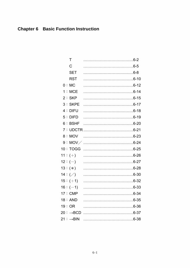
Chapter 6 Basic Function Instruction T …………………………………6-2
C …………………………………6-5
SET …………………………………6-8
RST …………………………………6-10
0: MC …………………………………6-12
1: MCE …………………………………6-14
2: SKP …………………………………6-15
3: SKPE …………………………………6-17
4: DIFU …………………………………6-18
5: DIFD …………………………………6-19
6: BSHF …………………………………6-20
7: UDCTR …………………………………6-21
8: MOV …………………………………6-23
9: MOV/ …………………………………6-24
10: TOGG …………………………………6-25
11: (+) …………………………………6-26
12: (-) …………………………………6-27
13: (*) …………………………………6-28
14: (/) …………………………………6-30
15: (+1) …………………………………6-32
16: (-1) …………………………………6-33
17: CMP …………………………………6-34
18: AND …………………………………6-35
19: OR …………………………………6-36
20: →BCD …………………………………6-37
21: →BIN …………………………………6-38
Basic Function Instruction
6-2
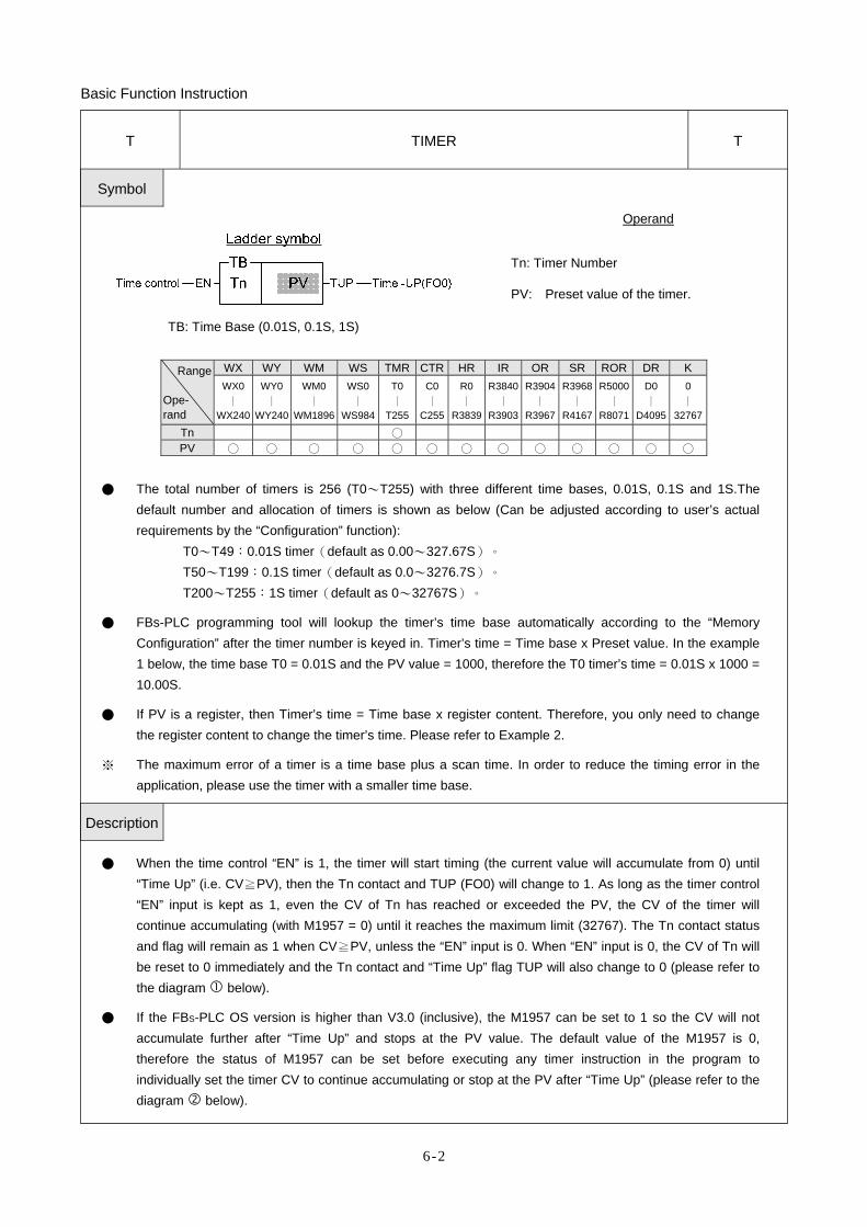
T TIMER T
Symbol
TB: Time Base (0.01S, 0.1S, 1S)
Operand
Tn: Timer Number
PV: Preset value of the timer.
Range
Ope- rand
WX WY WM WS TMR CTR HR IR OR SR ROR DR K WX0
∣ WX240
WY0 ∣
WY240
WM0 ∣
WM1896
WS0∣
WS984
T0 ∣
T255
C0∣
C255
R0 ∣
R3839
R3840∣
R3903
R3904∣
R3967
R3968∣
R4167
R5000 ∣
R8071
D0 ∣
D4095
0 ∣
32767
Tn ○ PV ○ ○ ○ ○ ○ ○ ○ ○ ○ ○ ○ ○ ○
● The total number of timers is 256 (T0~T255) with three different time bases, 0.01S, 0.1S and 1S.The
default number and allocation of timers is shown as below (Can be adjusted according to user’s actual requirements by the “Configuration” function):
T0~T49:0.01S timer(default as 0.00~327.67S)。 T50~T199:0.1S timer(default as 0.0~3276.7S)。 T200~T255:1S timer(default as 0~32767S)。
● FBs-PLC programming tool will lookup the timer’s time base automatically according to the “Memory Configuration” after the timer number is keyed in. Timer’s time = Time base x Preset value. In the example 1 below, the time base T0 = 0.01S and the PV value = 1000, therefore the T0 timer’s time = 0.01S x 1000 = 10.00S.
● If PV is a register, then Timer’s time = Time base x register content. Therefore, you only need to change the register content to change the timer’s time. Please refer to Example 2.
※ The maximum error of a timer is a time base plus a scan time. In order to reduce the timing error in the application, please use the timer with a smaller time base.
Description
● When the time control “EN” is 1, the timer will start timing (the current value will accumulate from 0) until “Time Up” (i.e. CV≧PV), then the Tn contact and TUP (FO0) will change to 1. As long as the timer control “EN” input is kept as 1, even the CV of Tn has reached or exceeded the PV, the CV of the timer will continue accumulating (with M1957 = 0) until it reaches the maximum limit (32767). The Tn contact status and flag will remain as 1 when CV≧PV, unless the “EN” input is 0. When “EN” input is 0, the CV of Tn will be reset to 0 immediately and the Tn contact and “Time Up” flag TUP will also change to 0 (please refer to the diagram below).
● If the FBS-PLC OS version is higher than V3.0 (inclusive), the M1957 can be set to 1 so the CV will not accumulate further after “Time Up” and stops at the PV value. The default value of the M1957 is 0, therefore the status of M1957 can be set before executing any timer instruction in the program to individually set the timer CV to continue accumulating or stop at the PV after “Time Up” (please refer to the diagram below).
Basic Function Instruction
6-3
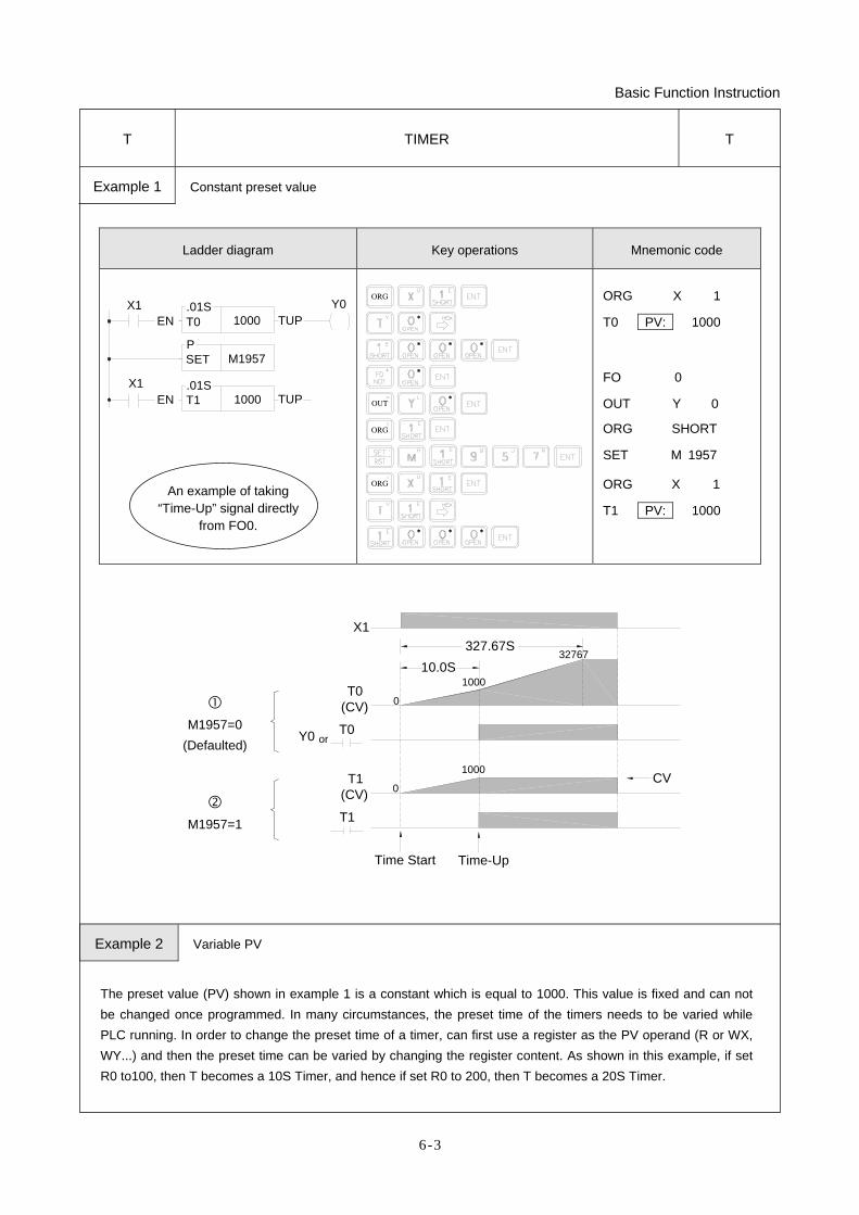
Ladder diagram Key operations Mnemonic code
P
X1
EN
EN
.01S
.01S
T0 1000
SET M1957
T1 1000
X1 Y0TUP
TUP
An example of taking “Time-Up” signal directly
from FO0.
ORG
ORG
OUT
ORG ORG X 1
T0 PV: 1000
FO 0
OUT Y 0
ORG SHORT
SET M 1957
ORG X 1
T1 PV: 1000
M1957=0
(Defaulted)
M1957=1
X1
T0(CV)
Y0 T0
T1
T1(CV)
or
1000
0
0
32767
1000CV
Time Start Time-Up
10.0S327.67S
Example 2 Variable PV
The preset value (PV) shown in example 1 is a constant which is equal to 1000. This value is fixed and can not be changed once programmed. In many circumstances, the preset time of the timers needs to be varied while PLC running. In order to change the preset time of a timer, can first use a register as the PV operand (R or WX, WY...) and then the preset time can be varied by changing the register content. As shown in this example, if set R0 to100, then T becomes a 10S Timer, and hence if set R0 to 200, then T becomes a 20S Timer.
T TIMER T
Example 1 Constant preset value
Basic Function Instruction
6-4
T TIMER T
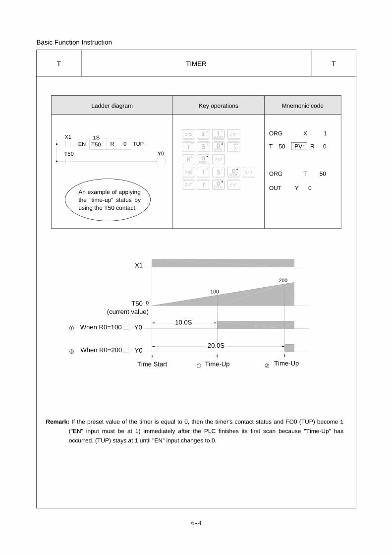
Ladder diagram Key operations Mnemonic code
X1EN TUP
.1S
Y0T50
T50 R 0
An example of applying the “time-up” status by using the T50 contact.
ORG X 1
T 50 PV: R 0
ORG T 50
OUT Y 0
X1
T50
When R0=100
When R0=200
Time Start Time-Up Time-Up
(current value)10.0S
20.0S
Y0
Y0
0
100
200
Remark: If the preset value of the timer is equal to 0, then the timer's contact status and FO0 (TUP) become 1
("EN" input must be at 1) immediately after the PLC finishes its first scan because "Time-Up" has occurred. (TUP) stays at 1 until "EN" input changes to 0.
Basic Function Instruction
6-5
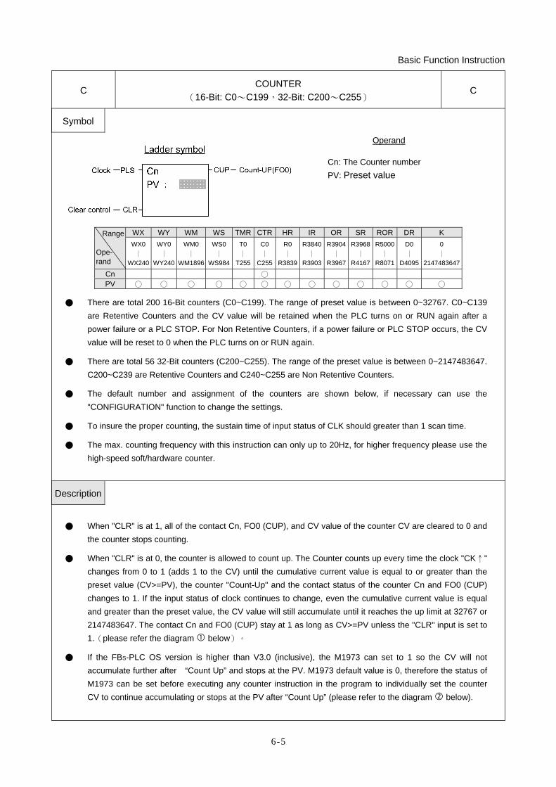
C COUNTER
(16-Bit: C0~C199,32-Bit: C200~C255) C
Symbol
Operand Cn: The Counter number PV: Preset value
Range
Ope- rand
WX WY WM WS TMR CTR HR IR OR SR ROR DR K WX0
∣ WX240
WY0∣
WY240
WM0 ∣
WM1896
WS0 ∣
WS984
T0∣
T255
C0∣
C255
R0 ∣
R3839
R3840∣
R3903
R3904∣
R3967
R3968∣
R4167
R5000 ∣
R8071
D0 ∣
D4095
0 ∣
2147483647
Cn ○ PV ○ ○ ○ ○ ○ ○ ○ ○ ○ ○ ○ ○ ○
● There are total 200 16-Bit counters (C0~C199). The range of preset value is between 0~32767. C0~C139 are Retentive Counters and the CV value will be retained when the PLC turns on or RUN again after a power failure or a PLC STOP. For Non Retentive Counters, if a power failure or PLC STOP occurs, the CV value will be reset to 0 when the PLC turns on or RUN again.
● There are total 56 32-Bit counters (C200~C255). The range of the preset value is between 0~2147483647. C200~C239 are Retentive Counters and C240~C255 are Non Retentive Counters.
● The default number and assignment of the counters are shown below, if necessary can use the "CONFIGURATION" function to change the settings.
● To insure the proper counting, the sustain time of input status of CLK should greater than 1 scan time.
● The max. counting frequency with this instruction can only up to 20Hz, for higher frequency please use the high-speed soft/hardware counter.
Description
● When "CLR" is at 1, all of the contact Cn, FO0 (CUP), and CV value of the counter CV are cleared to 0 and
the counter stops counting.
● When "CLR" is at 0, the counter is allowed to count up. The Counter counts up every time the clock "CK↑" changes from 0 to 1 (adds 1 to the CV) until the cumulative current value is equal to or greater than the preset value (CV>=PV), the counter "Count-Up" and the contact status of the counter Cn and FO0 (CUP) changes to 1. If the input status of clock continues to change, even the cumulative current value is equal and greater than the preset value, the CV value will still accumulate until it reaches the up limit at 32767 or 2147483647. The contact Cn and FO0 (CUP) stay at 1 as long as CV>=PV unless the "CLR" input is set to 1.(please refer the diagram below)。
● If the FBS-PLC OS version is higher than V3.0 (inclusive), the M1973 can set to 1 so the CV will not accumulate further after “Count Up” and stops at the PV. M1973 default value is 0, therefore the status of M1973 can be set before executing any counter instruction in the program to individually set the counter CV to continue accumulating or stops at the PV after “Count Up” (please refer to the diagram below).
Basic Function Instruction
6-6
C COUNTER
(16-Bit: C0~C199, 32-bit: C200~C255) C
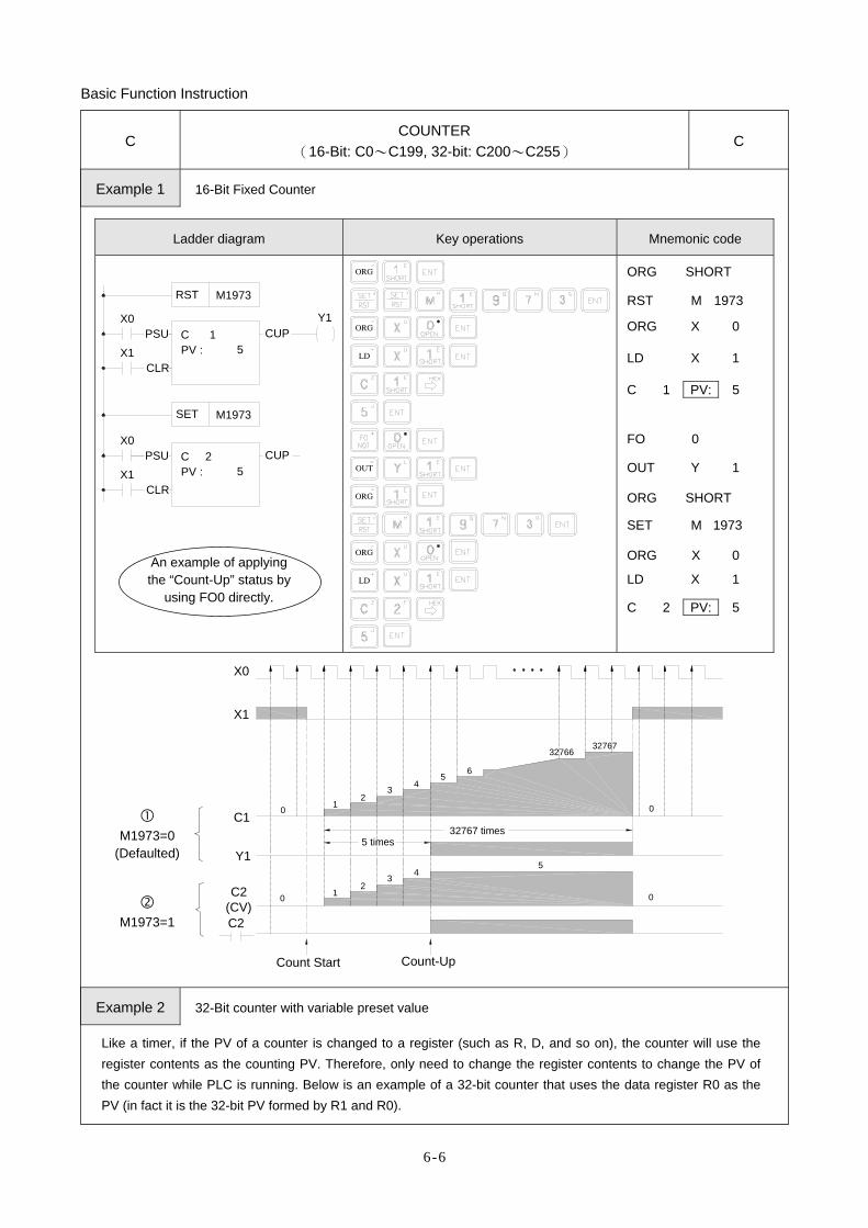
Example 1 16-Bit Fixed Counter
Ladder diagram Key operations Mnemonic code
C 1PV :
X0
SET M1973
CUPY1
RST M1973
X1CLR
5
C 2PV :
X0CUP
X1CLR
5
PSU
PSU
An example of applying the “Count-Up” status by
using FO0 directly.
ORG
LD
ORG
OUT
LD
ORG
ORG ORG SHORT
RST M 1973
ORG X 0
LD X 1
C 1 PV: 5
FO 0
OUT Y 1
ORG SHORT
SET M 1973
ORG X 0
LD X 1
C 2 PV: 5
M1973=0
(Defaulted)
M1973=1
Count Start Count-Up
X0
X1
C1
Y1
C2
C2(CV)
0
0
12
34
56
12
34
3276632767
0
0
5
5 times32767 times
Example 2 32-Bit counter with variable preset value Like a timer, if the PV of a counter is changed to a register (such as R, D, and so on), the counter will use the register contents as the counting PV. Therefore, only need to change the register contents to change the PV of the counter while PLC is running. Below is an example of a 32-bit counter that uses the data register R0 as the PV (in fact it is the 32-bit PV formed by R1 and R0).
Basic Function Instruction
6-7
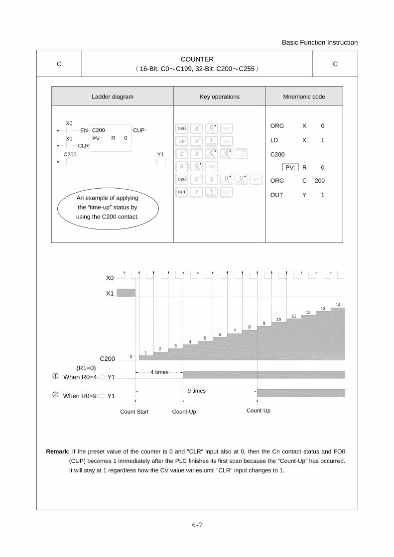
C COUNTER
(16-Bit: C0~C199, 32-Bit: C200~C255) C
Ladder diagram Key operations Mnemonic code
PV : R 0
X0
C200 Y1
X1CLR
C200EN CUP
An example of applying the “time-up” status by
using the C200 contact.
ORG
OUT
LD
ORG
ORG X 0
LD X 1
C200
PV: R 0
ORG C 200
OUT Y 1
X0
X1
C200(R1=0)
When R0=4
When R0=9
Y1
Y1
Count Start Count-Up
4 times
9 times
Count-Up
01
23
45
67
89
1011
1213
14
Remark: If the preset value of the counter is 0 and "CLR" input also at 0, then the Cn contact status and FO0 (CUP) becomes 1 immediately after the PLC finishes its first scan because the "Count-Up" has occurred. It will stay at 1 regardless how the CV value varies until "CLR" input changes to 1.
Basic Function Instruction
6-8
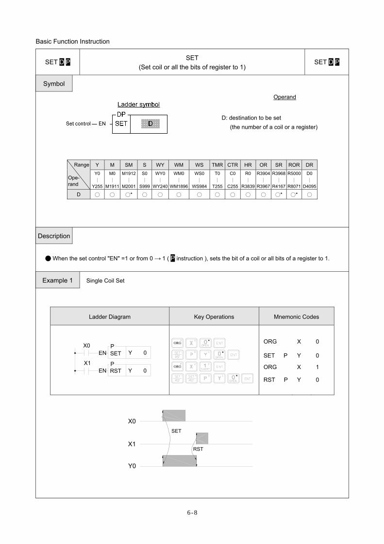
SET D P SET (Set coil or all the bits of register to 1)
SET D P
Symbol
Operand
D: destination to be set (the number of a coil or a register)
Range
Ope- rand
Y M SM S WY WM WS TMR CTR HR OR SR ROR DR Y0 ∣
Y255
M0∣
M1911
M1912 ∣
M2001
S0 ∣
S999
WY0∣
WY240
WM0∣
WM1896
WS0 ∣
WS984
T0∣
T255
C0∣
C255
R0∣
R3839
R3904∣
R3967
R3968 ∣
R4167
R5000 ∣
R8071
D0 ∣
D4095
D ○ ○ ○* ○ ○ ○ ○ ○ ○ ○ ○ ○* ○* ○
Description
● When the set control "EN" =1 or from 0 → 1 ( P instruction ), sets the bit of a coil or all bits of a register to 1.
Example 1 Single Coil Set
Ladder Diagram Key Operations Mnemonic Codes
PSET Y 0
X0
X1RSTP
Y 0EN
EN
ORG
ORG
ORG
SET P
ORG
RST P
X
Y
X
Y
0
0
1
0
X0
X1
Y0
SET
RST
Basic Function Instruction
6-9
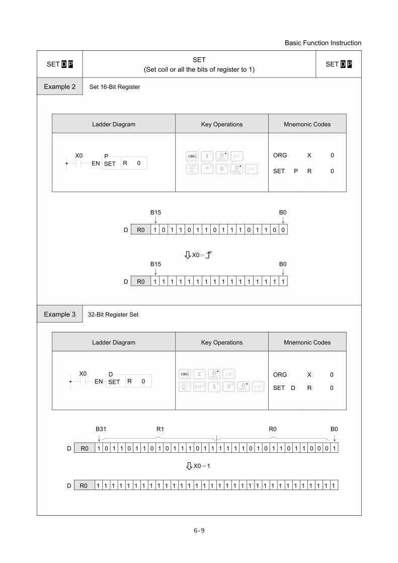
SET D P SET
(Set coil or all the bits of register to 1) SET D P
Example 2 Set 16-Bit Register
Ladder Diagram Key Operations Mnemonic Codes
PSET R 0
X0EN
ORG
ORG
SET P
X
R
0
0
B15 B0 ↓ ↓
D R0 1 0 1 1 0 1 1 0 1 1 1 0 1 1 0 0
X0= B15 B0 ↓ ↓
D R0 1 1 1 1 1 1 1 1 1 1 1 1 1 1 1 1
Example 3 32-Bit Register Set
Ladder Diagram Key Operations Mnemonic Codes
SET R 0X0
END
ORG
ORG
SET D
X
R
0
0
B31 R1 R0 B0 ↓ ∣ ↓
D R0 1 0 1 1 0 1 1 0 1 0 1 1 1 0 1 1 1 1 1 1 0 1 0 1 1 0 1 1 0 0 0 1
X0=1
D R0 1 1 1 1 1 1 1 1 1 1 1 1 1 1 1 1 1 1 1 1 1 1 1 1 1 1 1 1 1 1 1 1
Basic Function Instruction
6-10
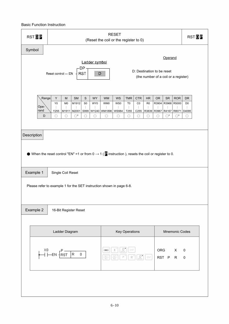
RST D P RESET (Reset the coil or the register to 0)
RST D P
Symbol
Operand
D: Destination to be reset (the number of a coil or a register)
Range
Ope- rand
Y M SM S WY WM WS TMR CTR HR OR SR ROR DR Y0 ∣
Y255
M0 ∣
M1911
M1912 ∣
M2001
S0 ∣
S999
WY0∣
WY240
WM0∣
WM1896
WS0∣
WS984
T0 ∣
T255
C0 ∣
C255
R0 ∣
R3839
R3904 ∣
R3967
R3968 ∣
R4167
R5000 ∣
R8071
D0 ∣
D4095
D ○ ○ ○* ○ ○ ○ ○ ○ ○ ○ ○ ○* ○* ○
Description
● When the reset control "EN" =1 or from 0 → 1 ( P instruction ), resets the coil or register to 0.
Example 1 Single Coil Reset
Please refer to example 1 for the SET instruction shown in page 6-8.
Example 2 16-Bit Register Reset
Ladder Diagram Key Operations Mnemonic Codes
ORG ORG X 0
RST P R 0
Basic Function Instruction
6-11
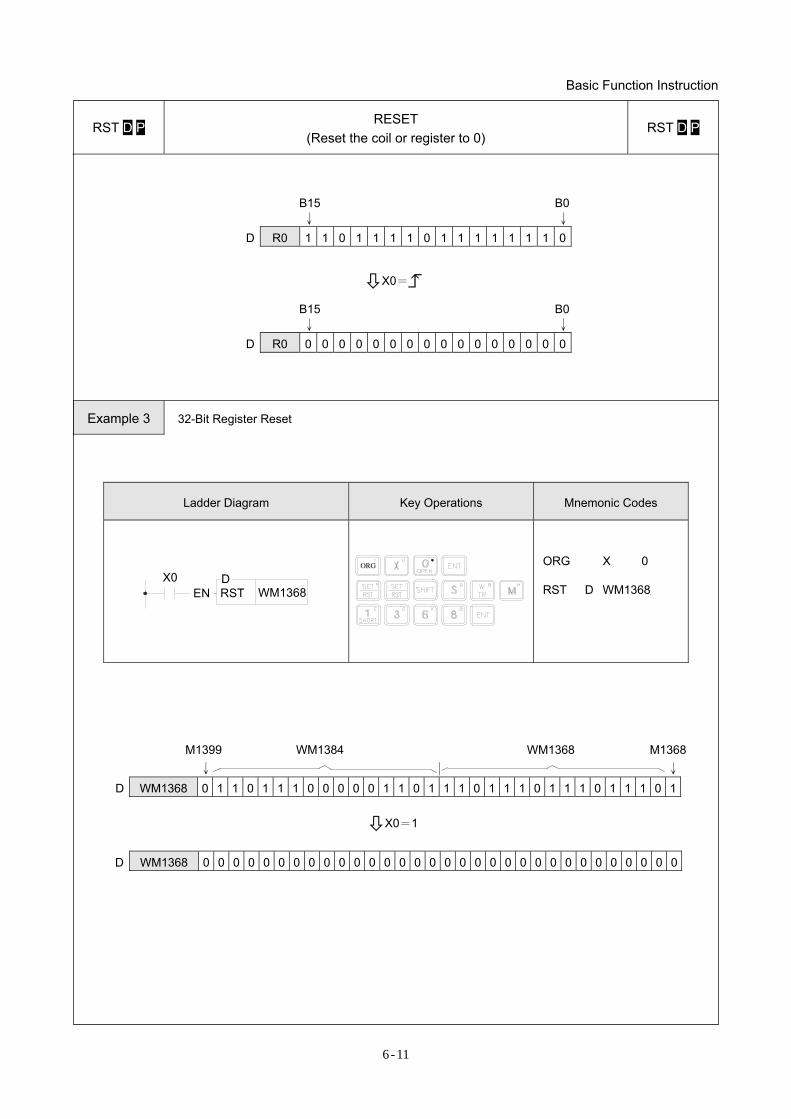
RST D P RESET (Reset the coil or register to 0)
RST D P
B15 B0 ↓ ↓
D R0 1 1 0 1 1 1 1 0 1 1 1 1 1 1 1 0
X0=
B15 B0 ↓ ↓
D R0 0 0 0 0 0 0 0 0 0 0 0 0 0 0 0 0
Example 3 32-Bit Register Reset
Ladder Diagram Key Operations Mnemonic Codes
DX0EN RST WM1368
ORG
ORG X 0
RST D WM1368
M1399 WM1384 WM1368 M1368 ↓ ∣ ↓
D WM1368 0 1 1 0 1 1 1 0 0 0 0 0 1 1 0 1 1 1 0 1 1 1 0 1 1 1 0 1 1 1 0 1
X0=1
D WM1368 0 0 0 0 0 0 0 0 0 0 0 0 0 0 0 0 0 0 0 0 0 0 0 0 0 0 0 0 0 0 0 0
Basic Function Instruction
6-12
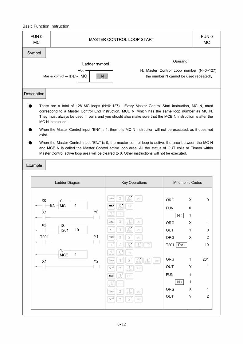
FUN 0 MC
MASTER CONTROL LOOP START FUN 0
MC
Symbol
MCENMaster control
Ladder symbol 0.
N
Operand N: Master Control Loop number (N=0~127)
the number N cannot be used repeatedly.
Description
● There are a total of 128 MC loops (N=0~127). Every Master Control Start instruction, MC N, must correspond to a Master Control End instruction, MCE N, which has the same loop number as MC N. They must always be used in pairs and you should also make sure that the MCE N instruction is after the MC N instruction.
● When the Master Control input "EN/" is 1, then this MC N instruction will not be executed, as it does not exist.
● When the Master Control input "EN/" is 0, the master control loop is active, the area between the MC N and MCE N is called the Master Control active loop area. All the status of OUT coils or Timers within Master Control active loop area will be cleared to 0. Other instructions will not be executed.
Example
Ladder Diagram Key Operations Mnemonic Codes
0.MC 1
X0EN
X1
1ST201 10
X2
T201
1.MCE 1
X1 Y2
Y1
Y0
OUT
ORG
ORG
OUT
ORG
ORG
OUT
ORG
ORG
FUN
N:
ORG
OUT
ORG
T201 PV:
ORG
OUT
FUN
N:
ORG
OUT
X
0
1
X
Y
X
T
Y
1
1
X
Y
0
1
0
2
10
201
1
1
2
Basic Function Instruction
6-13
FUN 0 MC
MASTER CONTROL LOOP START FUN 0
MC
X0
X1
X2
T201
Y0
Y1
Y2
10S
10
0
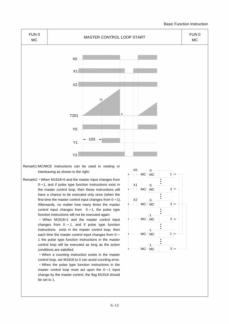
Remark1:MC/MCE instructions can be used in nesting or interleaving as shown to the right:
Remark2:‧When M1918=0 and the master input changes from 0→1, and if pulse type function instructions exist in the master control loop, then these instructions will have a chance to be executed only once (when the first time the master control input changes from 0→1). Afterwards, no matter how many times the master control input changes from 0→1, the pulse type function instructions will not be executed again. ‧When M1918=1 and the master control input changes from 0 → 1, and if pulse type function instructions exist in the master control loop, then each time the master control input changes from 0→1 the pulse type function instructions in the master control loop will be executed as long as the action conditions are satisfied. ‧When a counting instruction exists in the master control loop, set M1918 to 0 can avoid counting error. ‧When the pulse type function instructions in the master control loop must act upon the 0→1 input change by the master control, the flag M1918 should be set to 1.
0.MC 1
X0MC
0.MC 2
X1
0.MC 3
X2
1.MC 2
1.MC 1
1.MC 3
MC
MC
MC
MC
MC
Basic Function Instruction
6-14
FUN 1 MCE
MASTER CONTROL LOOP END FUN 1 MCE
Symbol
MCE
Ladder symbol 1.
N
Operand
N: Master Control End number (N=0~127) N can not be used repeatedly.
Description
● Every MCE N must correspond to a Master Control Start instruction. They must always be used as a pair and you should also make sure that the MCE N instruction is after the MC N instruction. After the MC N instruction has been executed, all output coil status and timers will be cleared to 0 and no other instructions will be executed. The program execution will resume until a MCE instruction which has the same N number as MC N instruction appears.
● MCE instruction does not require an input control because the instruction itself forms a network which other
instructions can not connect to it. If the MC instruction has been executed then the master control operation will be completed when the execution of the program reaches the MCE instruction. If MC N instruction has never been executed then the MCE instruction will do nothing.
Description
● Please refer to the example and explanations for MC instruction.
Basic Function Instruction
6-15
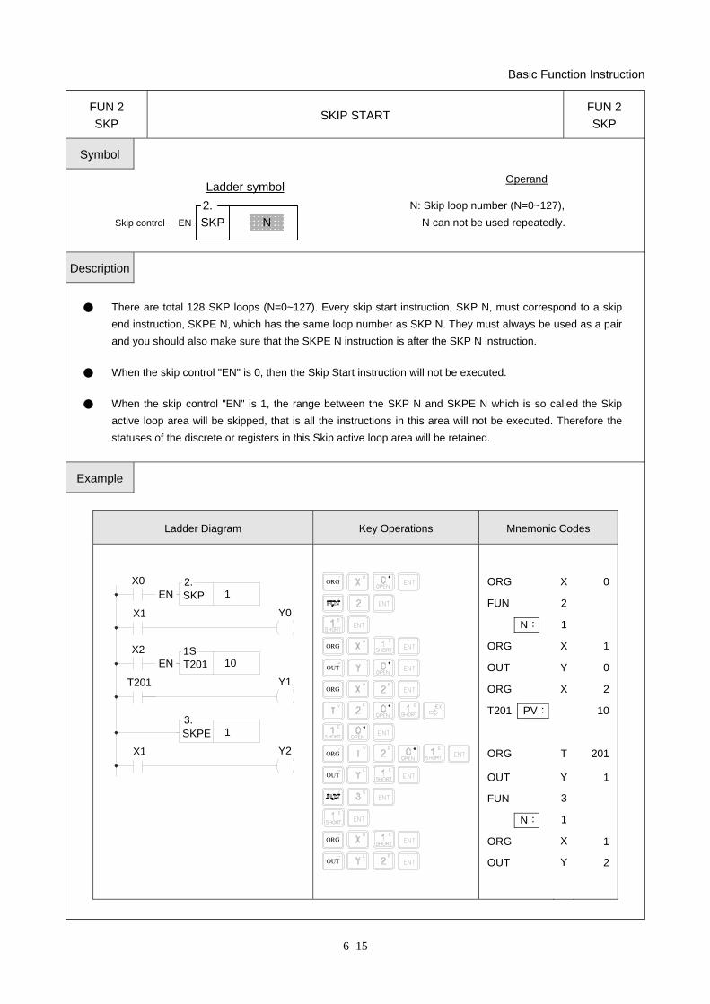
FUN 2 SKP
SKIP START FUN 2 SKP
Symbol
SKPENSkip control
Ladder symbol 2.
N
Operand
N: Skip loop number (N=0~127), N can not be used repeatedly.
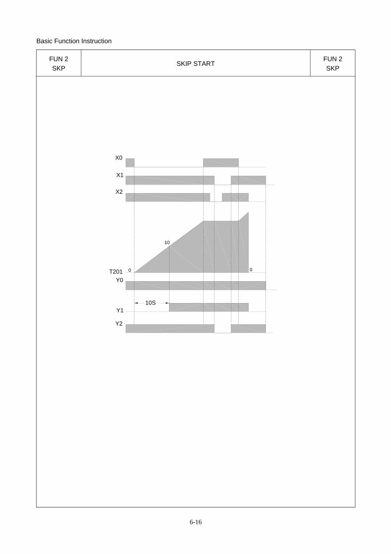
Description
● There are total 128 SKP loops (N=0~127). Every skip start instruction, SKP N, must correspond to a skip end instruction, SKPE N, which has the same loop number as SKP N. They must always be used as a pair and you should also make sure that the SKPE N instruction is after the SKP N instruction.
● When the skip control "EN" is 0, then the Skip Start instruction will not be executed.
● When the skip control "EN" is 1, the range between the SKP N and SKPE N which is so called the Skip
active loop area will be skipped, that is all the instructions in this area will not be executed. Therefore the statuses of the discrete or registers in this Skip active loop area will be retained.
Example
Ladder Diagram Key Operations Mnemonic Codes
1X0
Y0X1
1ST201 10
X2
Y1T201
1
Y2X1
2.
3.
EN
EN
SKP
SKPE
ORG
OUT
OUT
ORG
OUT
ORG
ORG
ORG
ORG
FUN
N:
ORG
OUT
ORG
T201 PV:
ORG
OUT
FUN
N:
ORG
OUT
X
2
1
X
Y
X
T
Y
3
1
X
Y
0
1
0
2
10
201
1
1
2
Basic Function Instruction
6-16
FUN 2 SKP
SKIP START FUN 2 SKP
Y2
Y1
Y0T201
10S
X0
X1
X2
0
10
0
Basic Function Instruction
6-17
FUN 3 SKPE
SKIP END FUN 3 SKPE
Symbol
SKPE
Ladder symbol 3.
N
Operand N: SKIP END Loop number (N=0~127) N
can not be used repeatedly.
Description
● Every SKPE N must correspond to a SKP N instruction. They must always be used as a pair and you should also make sure that the SKPE N instruction is behind the SKP N instruction.
● SKPE instruction does not require an input control because the instruction itself forms a network which
other instructions can not connect to it. If the SKP N instruction has been executed then the skip operation will be completed when the execution of the program reaches the SKPE N instruction. If SKP N instruction has never been executed then the SKPE instruction will do nothing.
Example
● Please refer to the example and explanations for SKP N instruction.
Remark : SKP/SKPE instructions can be used by nesting or interleaving. The coding rules are the same as for the MC/MCE instructions. Please refer to the section of MC/MCE instructions.
Basic Function Instruction
6-18
FUN 4 DIFU
DIFFERENTIAL UP FUN 4 DIFU
Symbol
Operand
D: a specific coil number where the result of the Differential Up operation is stored.
Range
Ope- rand
Y M SM S Y0 ∣
Y255
M0 ∣
M1911
M1912∣
M2001
S0 ∣
S999D ○ ○ ○* ○
Description
● The DIFU instruction is used to output the up differentiation of a node status (status input to "TGU") and the
pulse signal resulting from the status change at the rising edge of the "TGU" for one scan time is stored to a coil specified by D.
● The functionality of this instruction can also be achieved by using a TU contact.
Example The results of the following two samples are exactly the same
Ladder Diagram Key Operations Mnemonic Codes
Example 1
DIFU Y 0X1
TGU4P.
ORG
FUN
ORG
FUN
D:
X
4
Y
1
0
Example 2
Y0X1OUT
ORG
ORG TU
OUT
X
Y
1
0
X1
Y0
t t : scan time
Basic Function Instruction
6 -19
FUN 5 P DIFD
DIFFERENTIAL DOWN FUN 5 P
DIFD
Symbol
Operand
N: a specific coil number where the result of the Differential Down operation is stored.
Range
Ope- rand
Y M SM SY0∣
Y255
M0∣
M1911
M1912∣
M2001
S0∣
S999D ○ ○ ○* ○
Description
● The DIFD instruction is used to output the down differentiation of a node status (status input to "TGD") and the pulse signal resulting from the status change at the falling edge of the "TGD" for one scan time is stored to a coil specified by D.
● The functionality of this instruction can also be achieved by using a TD contact.
Example The results of the following two samples are exactly the same
Ladder Diagram Key Operations Mnemonic Codes
Example 1
DIFD Y 0X1
TGD5P.
ORG
FUN
ORG X 1
FUN 5
D: Y 0
Example 2
Y0X1
ORG
OUT
ORG TD X 1
OUT Y 0
X1
Y0
t : scan timet
Basic Function Instruction
6-20
FUN 6 D P BSHF
BIT SHIFT (Shifts the data of the 16-bit or 32-bit register to left or to right by one bit)
FUN 6 D P BSHF
Symbol
Description
● When the status of clear control "CLR" is at 1, then the data of register D and FO0 will all be cleared to 0. Other input signals are all in effect.
● When the status of clear control is "CLR" at 0, then the shift operation is permissible. When the shift control
"EN" = 1 or from 0 →1 ( P instruction), the data of the register will be shifted to right (L/R=0) or to left (L/R=1) by one bit. The shifted-out bit (MSB when shift to left and LSB when shift to right) for both cases will be sent to FO0. The vacated bit space (LSB when shift to left and MSB when shift to right) due to shift operation will be filled in by the input status of fill-in bit "INB".
Example Shifts the 16-bit register data
Ladder diagram Key Operations Mnemonic Codes
X3
X2
6P.BSHFD :
INB
L/R
R 3 OTBX1
X4CLR
Y0EN
OUT
FUN
LD
LD
LD
ORG
ORG X 1
LD X 2
LD X 3
LD X 4
FUN 6P
D: R 3
FO 0
OUT Y 0
X3=1 (Left shift)
B15 B0 ← ← ← ← ← ← ← ← ← ← ← ← ← ← ← ← ← ← Y0 Shifts the 16-bit data to left by one bit X2
X3=0 (Right shift)
B15 B0 → → → → → → → → → → → → → → → → → → X2 Shifts the 16-bit data to right by one bit Y0
Range
Ope- rand
WY WM WS TMR CTR HR OR SR ROR DRWY0
∣ WY240
WM0∣
WM1896
WS0∣
WS984
T0 ∣
T255
C0∣
C255
R0 ∣
R3839
R3904 ∣
R3967
R3968 ∣
R4167
R5000∣
R8071
D0 ∣
D4095
D ○ ○ ○ ○ ○ ○ ○ ○* ○* ○
Operand D: The register number for shifting
Basic Function Instruction
6 -21
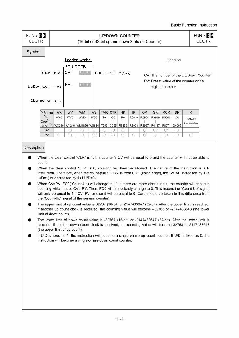
FUN 7 D P UDCTR
UP/DOWN COUNTER (16-bit or 32-bit up and down 2-phase Counter)
FUN 7 D P UDCTR
Symbol
Operand
CV: The number of the Up/Down Counter PV: Preset value of the counter or it's
register number
Range
Ope- rand
WX WY WM WS TMR CTR HR IR OR SR ROR DR K WX0
∣ WX240
WY0∣
WY240
WM0 ∣
WM1896
WS0 ∣
WS984
T0∣
T255
C0∣
C255
R0 ∣
R3839
R3840∣
R3903
R3904∣
R3967
R3968∣
R4167
R5000 ∣
R8071
D0 ∣
D4095
16/32-bit +/− number
CV ○ ○ ○ ○ ○ ○ ○ ○* ○* ○ PV ○ ○ ○ ○ ○ ○ ○ ○ ○ ○ ○ ○ ○
Description
● When the clear control “CLR” is 1, the counter’s CV will be reset to 0 and the counter will not be able to count.
● When the clear control “CLR” is 0, counting will then be allowed. The nature of the instruction is a P instruction. Therefore, when the count-pulse “PLS” is from 0→1 (rising edge), the CV will increased by 1 (if U/D=1) or decreased by 1 (if U/D=0).
● When CV=PV, FO0(“Count-Up) will change to 1”. If there are more clocks input, the counter will continue counting which cause CV≠PV. Then, FO0 will immediately change to 0. This means the “Count-Up” signal will only be equal to 1 if CV=PV, or else it will be equal to 0 (Care should be taken to this difference from the “Count-Up” signal of the general counter).
● The upper limit of up count value is 32767 (16-bit) or 2147483647 (32-bit). After the upper limit is reached, if another up count clock is received, the counting value will become –32768 or -2147483648 (the lower limit of down count).
● The lower limit of down count value is -32767 (16-bit) or -2147483647 (32-bit). After the lower limit is reached, if another down count clock is received, the counting value will become 32768 or 2147483648 (the upper limit of up count).
● If U/D is fixed as 1, the instruction will become a single-phase up count counter. If U/D is fixed as 0, the instruction will become a single-phase down count counter.
Basic Function Instruction
6-22
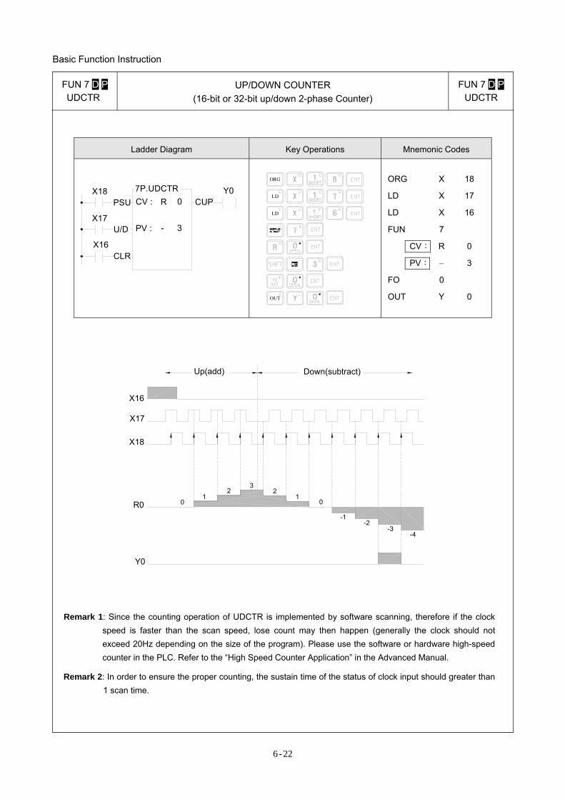
FUN 7 D P UDCTR
UP/DOWN COUNTER (16-bit or 32-bit up/down 2-phase Counter)
FUN 7 D P UDCTR
Ladder Diagram Key Operations Mnemonic Codes
X18
X16
CV :
PV :U/D
CLR
R 0
3
CUP
X17-
Y0PSU
7P.UDCTRORG
OUT
LD
LD
ORG X 18
LD X 17
LD X 16
FUN 7
CV: R 0
PV: − 3
FO 0
OUT Y 0
X16
X17
X18
R0
Y0
Up(add) Down(subtract)
01
23
21
0
-1-2
-3-4
Remark 1: Since the counting operation of UDCTR is implemented by software scanning, therefore if the clock speed is faster than the scan speed, lose count may then happen (generally the clock should not exceed 20Hz depending on the size of the program). Please use the software or hardware high-speed counter in the PLC. Refer to the “High Speed Counter Application” in the Advanced Manual.
Remark 2: In order to ensure the proper counting, the sustain time of the status of clock input should greater than 1 scan time.
Basic Function Instruction
6 -23
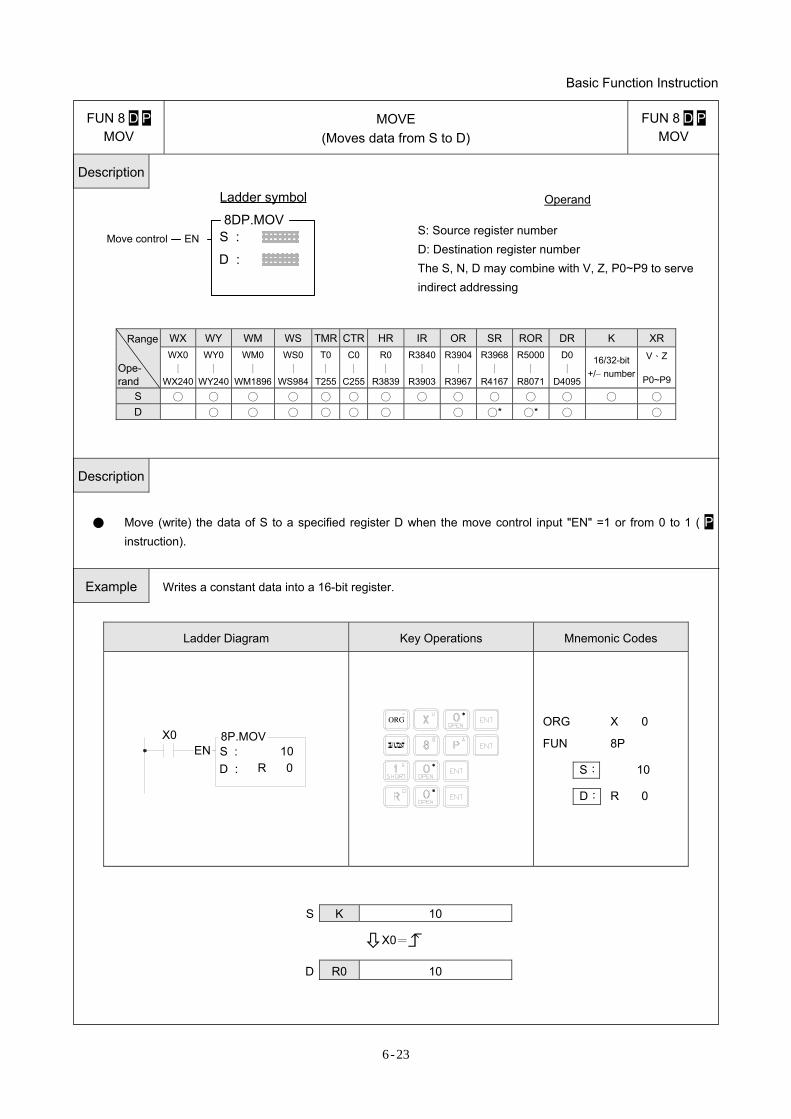
FUN 8 D P MOV
MOVE (Moves data from S to D)
FUN 8 D P MOV
Description
S :
D :ENMove control
Ladder symbol
8DP.MOV
Operand S: Source register number D: Destination register number The S, N, D may combine with V, Z, P0~P9 to serve indirect addressing
Range
Ope- rand
WX WY WM WS TMR CTR HR IR OR SR ROR DR K XRWX0
∣ WX240
WY0 ∣
WY240
WM0 ∣
WM1896
WS0 ∣
WS984
T0∣
T255
C0∣
C255
R0 ∣
R3839
R3840∣
R3903
R3904∣
R3967
R3968∣
R4167
R5000∣
R8071
D0 ∣
D4095
16/32-bit +/− number
V、Z
P0~P9
S ○ ○ ○ ○ ○ ○ ○ ○ ○ ○ ○ ○ ○ ○ D ○ ○ ○ ○ ○ ○ ○ ○* ○* ○ ○
Description
● Move (write) the data of S to a specified register D when the move control input "EN" =1 or from 0 to 1 ( P
instruction).
Example Writes a constant data into a 16-bit register.
Ladder Diagram Key Operations Mnemonic Codes
8P.MOVS :
R 0
X0
D :10EN
ORG
ORG X 0
FUN 8P
S: 10
D: R 0
S K 10
X0=
D R0 10
Basic Function Instruction
6-24
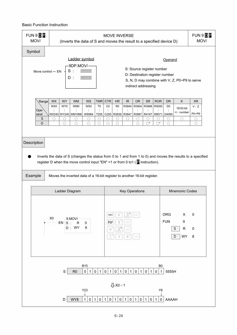
FUN 9 D P MOV/
MOVE INVERSE (Inverts the data of S and moves the result to a specified device D)
FUN 9 D P MOV/
Symbol
S :
D :ENMove control
Ladder symbol
9DP.MOV/
Operand S: Source register number D: Destination register number S, N, D may combine with V, Z, P0~P9 to serve indirect addressing
Range
Ope- rand
WX WY WM WS TMR CTR HR IR OR SR ROR DR K XR WX0
∣ WX240
WY0 ∣
WY240
WM0 ∣
WM1896
WS0 ∣
WS984
T0∣
T255
C0∣
C255
R0 ∣
R3839
R3840∣
R3847
R3904∣
R3967
R3968∣
R4167
R5000∣
R8071
D0 ∣
D4095
16/32-bit +/− number
V、Z
P0~P9
S ○ ○ ○ ○ ○ ○ ○ ○ ○ ○ ○ ○ ○ ○ D ○ ○ ○ ○ ○ ○ ○ ○* ○* ○ ○
Description
● Inverts the data of S (changes the status from 0 to 1 and from 1 to 0) and moves the results to a specified
register D when the move control input "EN" =1 or from 0 to1 ( P instruction).
Example Moves the inverted data of a 16-bit register to another 16-bit register.
Ladder Diagram Key Operations Mnemonic Codes
9.MOV/S : R 0
X0
D : WY 8EN
ORG
ORG X 0
FUN 9
S: R 0
D: WY 8
B15 B0
S R0 0 1 0 1 0 1 0 1 0 1 0 1 0 1 0 1 5555H
X0=1 Y23 Y8 ↓ ↓
D WY8 1 0 1 0 1 0 1 0 1 0 1 0 1 0 1 0 AAAAH
Basic Function Instruction
6-25
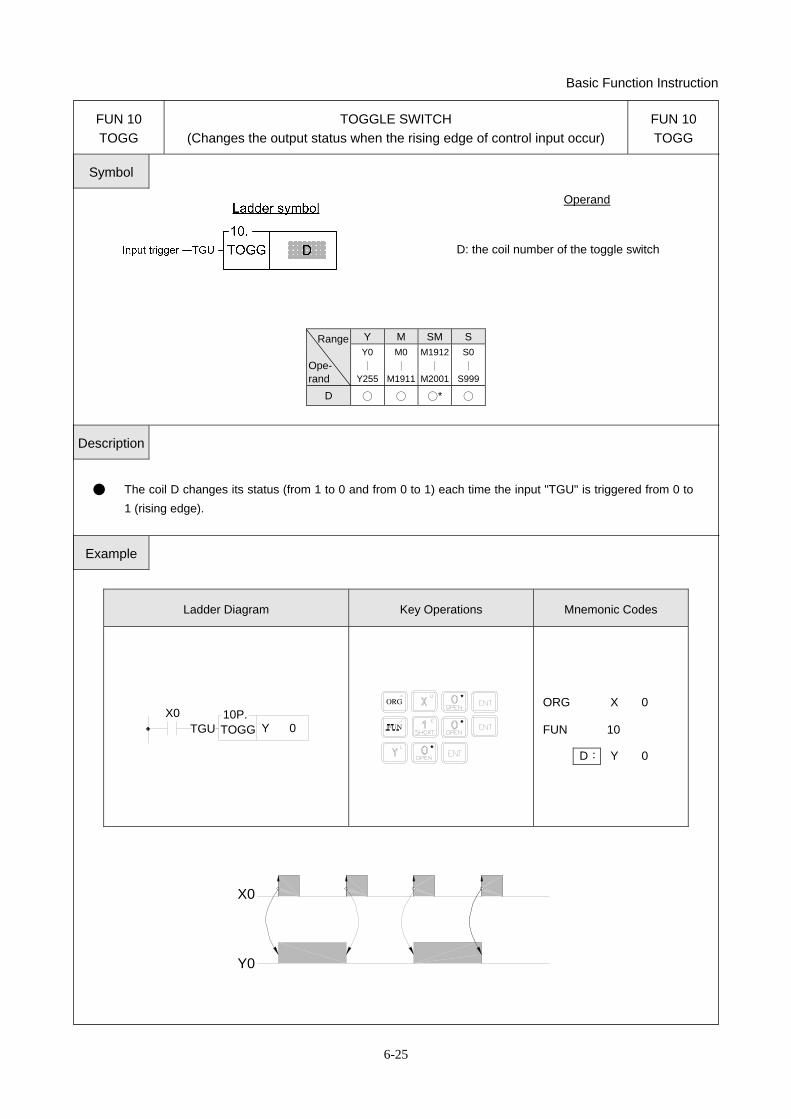
FUN 10 TOGG
TOGGLE SWITCH (Changes the output status when the rising edge of control input occur)
FUN 10 TOGG
Symbol
Operand D: the coil number of the toggle switch
Range
Ope- rand
Y M SM S Y0 ∣
Y255
M0∣
M1911
M1912∣
M2001
S0 ∣
S999
D ○ ○ ○* ○
Description
● The coil D changes its status (from 1 to 0 and from 0 to 1) each time the input "TGU" is triggered from 0 to
1 (rising edge).
Example
Ladder Diagram Key Operations Mnemonic Codes
10P.TOGG Y 0
X0TGU
ORG
ORG X 0
FUN 10
D: Y 0
X0
Y0
Basic Function Instruction
6-26
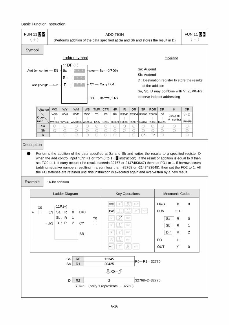
FUN 11 D P (+)
ADDITION (Performs addition of the data specified at Sa and Sb and stores the result in D)
FUN 11 D P(+)
Symbol
Operand Sa: Augend Sb: Addend D : Destination register to store the results
of the addition Sa, Sb, D may combine with V, Z, P0~P9 to serve indirect addressing
Range
Ope- rand
WX WY WM WS TMR CTR HR IR OR SR ROR DR K XRWX0
∣ WX240
WY0∣
WY240
WM0 ∣
WM1896
WS0 ∣
WS984
T0∣
T255
C0∣
C255
R0∣
R3839
R3840∣
R3903
R3904∣
R3967
R3968∣
R4167
R5000∣
R8071
D0 ∣
D4095
16/32-bit +/− number
V、Z P0~P9
Sa ○ ○ ○ ○ ○ ○ ○ ○ ○ ○ ○ ○ ○ ○ Sb ○ ○ ○ ○ ○ ○ ○ ○ ○ ○ ○ ○ ○ ○ D ○ ○ ○ ○ ○ ○ ○ ○* ○* ○ ○
Description
● Performs the addition of the data specified at Sa and Sb and writes the results to a specified register D when the add control input "EN" =1 or from 0 to 1 ( P instruction). If the result of addition is equal to 0 then set FO0 to 1. If carry occurs (the result exceeds 32767 or 2147483647) then set FO1 to 1. If borrow occurs (adding negative numbers resulting in a sum less than -32768 or -2147483648), then set the FO2 to 1. All the FO statuses are retained until this instruction is executed again and overwritten by a new result.
Example 16-bit addition
Ladder Diagram Key Operations Mnemonic Codes
X0Sa :Sb :D :
RRR
012
11P.(+)D=0
CY
BR
Y0U/S
EN
OUT
ORG
ORG X 0
FUN 11P
Sa: R 0
Sb: R 1
D: R 2
FO 1
OUT Y 0
Sa R0 12345
R0+R1=32770 Sb R1 20425
X0=
D R2 2 32768+2=32770 Y0=1 (carry 1 represents +32768)
Basic Function Instruction
6-27
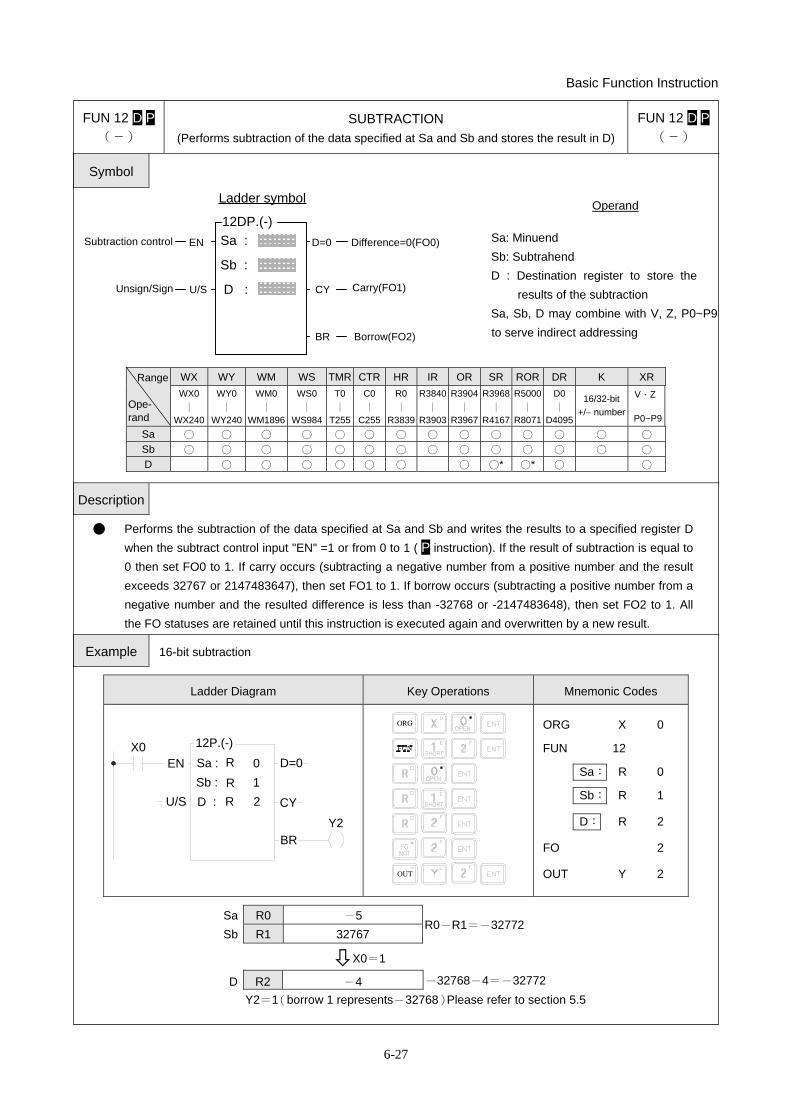
FUN 12 D P (−)
SUBTRACTION (Performs subtraction of the data specified at Sa and Sb and stores the result in D)
FUN 12 D P(−)
Symbol
Sa :ENSubtraction control D=0
Ladder symbol
12DP.(-)Difference=0(FO0)
CY Carry(FO1)
BR Borrow(FO2)
Sb :
D :U/SUnsign/Sign
Operand
Sa: Minuend Sb: Subtrahend D : Destination register to store the
results of the subtraction Sa, Sb, D may combine with V, Z, P0~P9to serve indirect addressing
Range
Ope- rand
WX WY WM WS TMR CTR HR IR OR SR ROR DR K XRWX0
∣ WX240
WY0∣
WY240
WM0 ∣
WM1896
WS0 ∣
WS984
T0∣
T255
C0∣
C255
R0∣
R3839
R3840∣
R3903
R3904∣
R3967
R3968∣
R4167
R5000∣
R8071
D0 ∣
D4095
16/32-bit +/− number
V、Z P0~P9
Sa ○ ○ ○ ○ ○ ○ ○ ○ ○ ○ ○ ○ ○ ○ Sb ○ ○ ○ ○ ○ ○ ○ ○ ○ ○ ○ ○ ○ ○ D ○ ○ ○ ○ ○ ○ ○ ○* ○* ○ ○
Description
● Performs the subtraction of the data specified at Sa and Sb and writes the results to a specified register D when the subtract control input "EN" =1 or from 0 to 1 ( P instruction). If the result of subtraction is equal to 0 then set FO0 to 1. If carry occurs (subtracting a negative number from a positive number and the result exceeds 32767 or 2147483647), then set FO1 to 1. If borrow occurs (subtracting a positive number from a negative number and the resulted difference is less than -32768 or -2147483648), then set FO2 to 1. All the FO statuses are retained until this instruction is executed again and overwritten by a new result.
Example 16-bit subtraction
Ladder Diagram Key Operations Mnemonic Codes
X0EN Sa :
Sb :D :
R
RR
012
12P.(-)
U/S
Y2BR
CY
D=0
OUT
ORG
ORG X 0
FUN 12
Sa: R 0
Sb: R 1
D: R 2
FO 2
OUT Y 2
Sa R0 -5
R0-R1=-32772 Sb R1 32767
X0=1
D R2 -4 -32768-4=-32772 Y2=1(borrow 1 represents-32768)Please refer to section 5.5
Basic Function Instruction
6-28
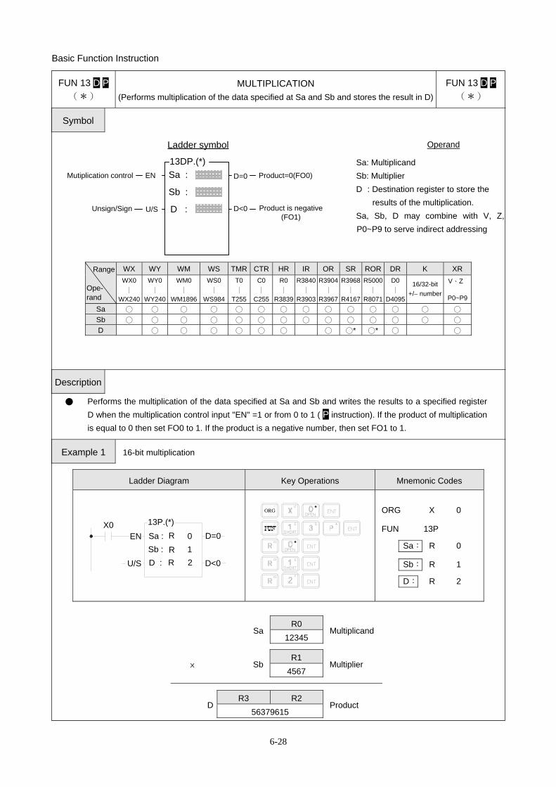
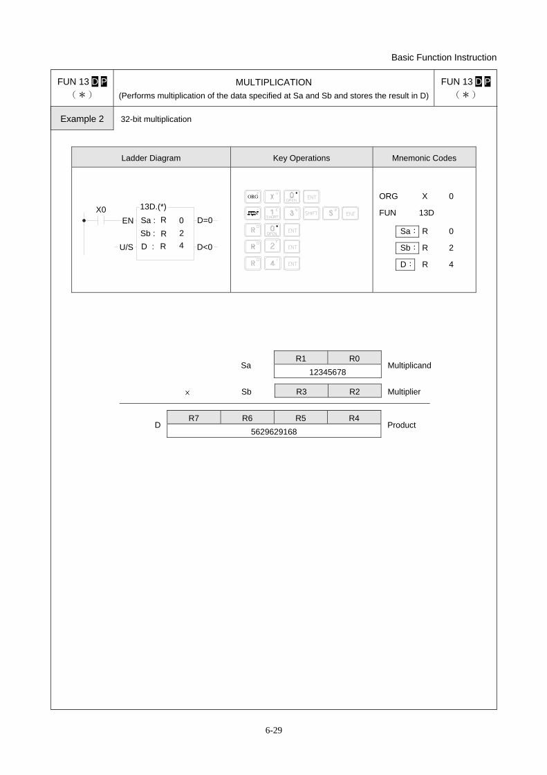
FUN 13 D P (*)
MULTIPLICATION (Performs multiplication of the data specified at Sa and Sb and stores the result in D)
FUN 13 D P (*)
Symbol
Sa :ENMutiplication control D=0
Ladder symbol
13DP.(*)Product=0(FO0)
D<0 Product is negative(FO1)
Sb :
D :U/SUnsign/Sign
Operand
Sa: Multiplicand Sb: Multiplier D : Destination register to store the
results of the multiplication. Sa, Sb, D may combine with V, Z, P0~P9 to serve indirect addressing
Range
Ope- rand
WX WY WM WS TMR CTR HR IR OR SR ROR DR K XR WX0
∣ WX240
WY0 ∣
WY240
WM0 ∣
WM1896
WS0 ∣
WS984
T0∣
T255
C0∣
C255
R0∣
R3839
R3840∣
R3903
R3904∣
R3967
R3968∣
R4167
R5000∣
R8071
D0 ∣
D4095
16/32-bit +/− number
V、Z P0~P9
Sa ○ ○ ○ ○ ○ ○ ○ ○ ○ ○ ○ ○ ○ ○ Sb ○ ○ ○ ○ ○ ○ ○ ○ ○ ○ ○ ○ ○ ○ D ○ ○ ○ ○ ○ ○ ○ ○* ○* ○ ○
Description
● Performs the multiplication of the data specified at Sa and Sb and writes the results to a specified register D when the multiplication control input "EN" =1 or from 0 to 1 ( P instruction). If the product of multiplication is equal to 0 then set FO0 to 1. If the product is a negative number, then set FO1 to 1.
Example 1 16-bit multiplication
Ladder Diagram Key Operations Mnemonic Codes
X0Sa :Sb :D :
R
RR
012
13P.(*)D=0
D<0U/S
EN
ORG
ORG X 0
FUN 13P
Sa: R 0
Sb: R 1
D: R 2
SaR0
Multiplicand 12345
× SbR1
Multiplier 4567
D R3 R2
Product 56379615
Basic Function Instruction
6-29
FUN 13 D P (*)
MULTIPLICATION (Performs multiplication of the data specified at Sa and Sb and stores the result in D)
FUN 13 D P(*)
Example 2 32-bit multiplication
Ladder Diagram Key Operations Mnemonic Codes
X0Sa :Sb :D :
R
RR
0
13D.(*)D=0
D<0U/S
24
EN
ORG
ORG X 0
FUN 13D
Sa: R 0
Sb: R 2
D: R 4
Sa R1 R0
Multiplicand 12345678
× Sb R3 R2 Multiplier
DR7 R6 R5 R4
Product 5629629168
Basic Function Instruction
6-30
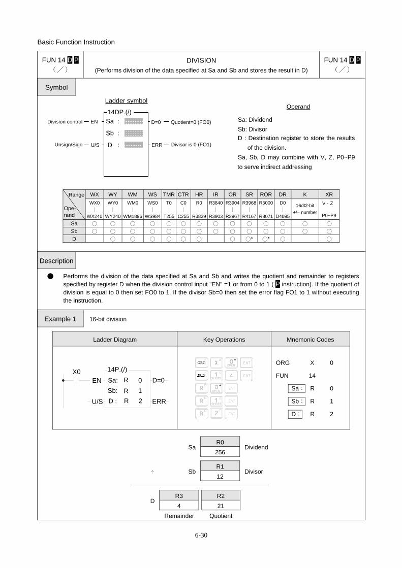
FUN 14 D P (/)
DIVISION (Performs division of the data specified at Sa and Sb and stores the result in D)
FUN 14 D P(/)
Symbol
Sa : ENDivision control D=0
Ladder symbol
14DP.(/)Quotient=0 (FO0)
ERR Divisor is 0 (FO1)
Sb :
D :U/SUnsign/Sign
Operand
Sa: Dividend Sb: Divisor D : Destination register to store the results
of the division. Sa, Sb, D may combine with V, Z, P0~P9 to serve indirect addressing
Range
Ope- rand
WX WY WM WS TMR CTR HR IR OR SR ROR DR K XR WX0
∣ WX240
WY0 ∣
WY240
WM0 ∣
WM1896
WS0 ∣
WS984
T0∣
T255
C0∣
C255
R0∣
R3839
R3840∣
R3903
R3904∣
R3967
R3968∣
R4167
R5000∣
R8071
D0 ∣
D4095
16/32-bit +/− number
V、Z P0~P9
Sa ○ ○ ○ ○ ○ ○ ○ ○ ○ ○ ○ ○ ○ ○ Sb ○ ○ ○ ○ ○ ○ ○ ○ ○ ○ ○ ○ ○ ○ D ○ ○ ○ ○ ○ ○ ○ ○* ○* ○ ○
Description
● Performs the division of the data specified at Sa and Sb and writes the quotient and remainder to registers specified by register D when the division control input "EN" =1 or from 0 to 1 ( P instruction). If the quotient of division is equal to 0 then set FO0 to 1. If the divisor Sb=0 then set the error flag FO1 to 1 without executing the instruction.
Example 1 16-bit division
Ladder Diagram Key Operations Mnemonic Codes
X0Sa:Sb:D :
R
RR
012
14P.(/)
U/S
EN
ERR
D=0
ORG
ORG X 0
FUN 14
Sa: R 0
Sb: R 1
D: R 2
SaR0
Dividend 256
÷ SbR1
Divisor 12
D R3 R2 4 21
Remainder Quotient
Basic Function Instruction
6-31
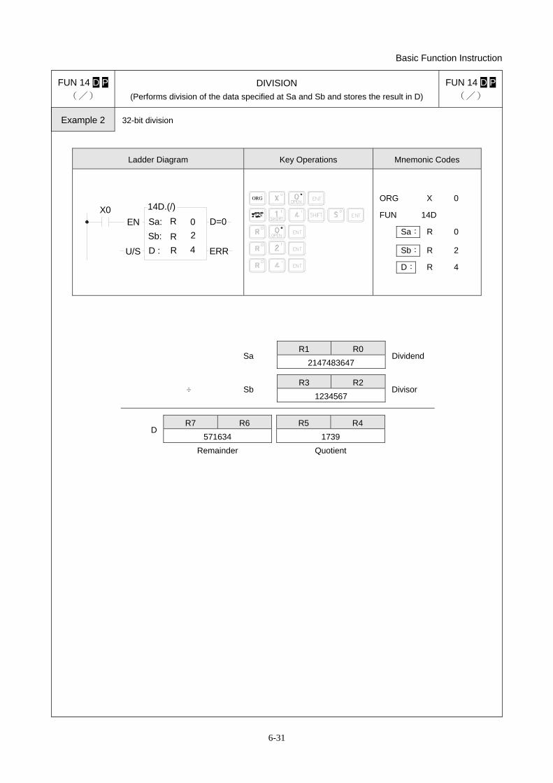
FUN 14 D P (/)
DIVISION (Performs division of the data specified at Sa and Sb and stores the result in D)
FUN 14 D P(/)
Example 2 32-bit division
Ladder Diagram Key Operations Mnemonic Codes
X0EN Sa:
Sb:D :
R
RR
02
D=0
ERRU/S 4
14D.(/)
ORG
ORG X 0
FUN 14D
Sa: R 0
Sb: R 2
D: R 4
Sa
R1 R0 Dividend
2147483647
÷ Sb R3 R2
Divisor 1234567
D R7 R6 R5 R4
571634 1739 Remainder Quotient
Basic Function Instruction
6-32
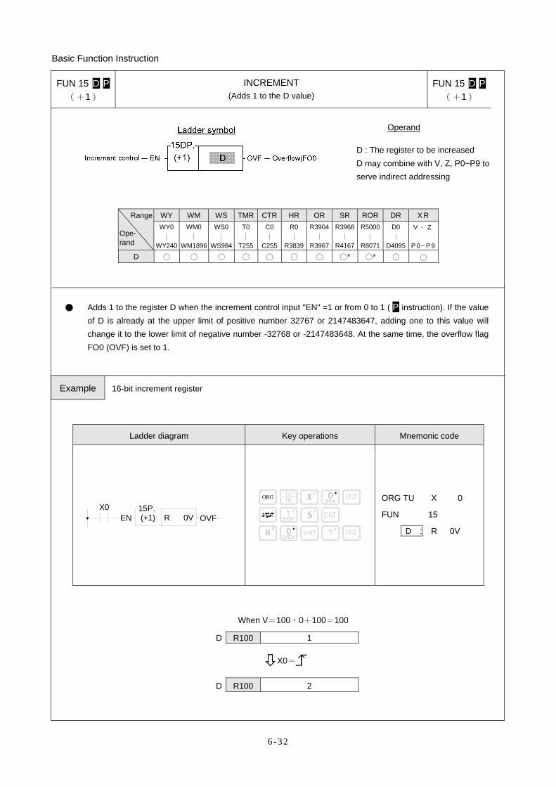
FUN 15 D P (+1)
INCREMENT (Adds 1 to the D value)
FUN 15 D P(+1)
Operand
D : The register to be increased D may combine with V, Z, P0~P9 to serve indirect addressing
Range
Ope- rand
WY WM WS TMR CTR HR OR SR ROR DR X R WY0
∣ WY240
WM0 ∣
WM1896
WS0 ∣
WS984
T0 ∣
T255
C0∣
C255
R0 ∣
R3839
R3904∣
R3967
R3968∣
R4167
R5000∣
R8071
D0 ∣
D4095
V、 Z
P 0 ~ P 9
D ○ ○ ○ ○ ○ ○ ○ ○* ○* ○ ○
● Adds 1 to the register D when the increment control input "EN" =1 or from 0 to 1 ( P instruction). If the value of D is already at the upper limit of positive number 32767 or 2147483647, adding one to this value will change it to the lower limit of negative number -32768 or -2147483648. At the same time, the overflow flag FO0 (OVF) is set to 1.
Example 16-bit increment register
Ladder diagram Key operations Mnemonic code
15P.(+1) R 0V
X0OVFEN
ORG
ORG TU X 0
FUN 15
D : R 0V
When V=100,0+100=100
D R100 1
X0=
D R100 2
Basic Function Instruction
6-33
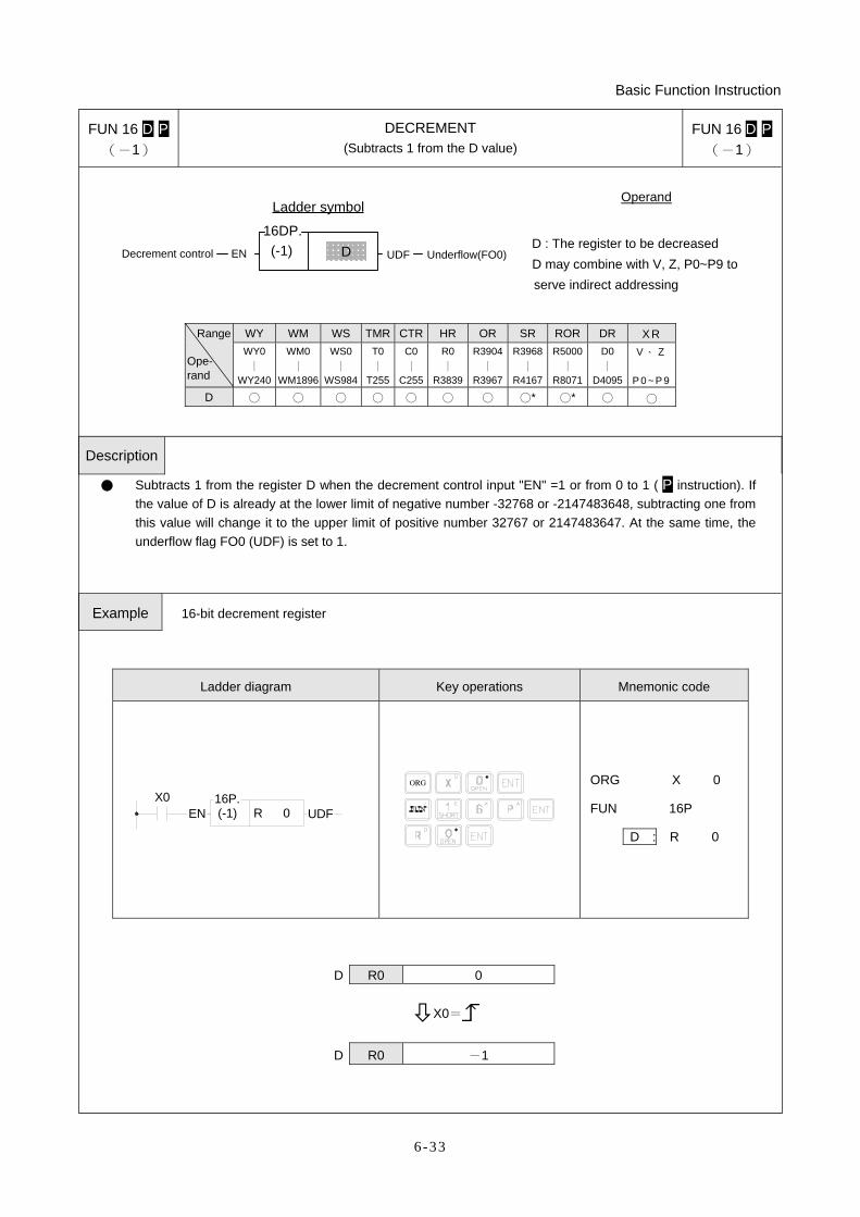
FUN 16 D P (-1)
DECREMENT (Subtracts 1 from the D value)
FUN 16 D P(-1)
(-1)
Ladder symbol
16DP.DENDecrement control UDF Underflow(FO0)
Operand
D : The register to be decreased D may combine with V, Z, P0~P9 to serve indirect addressing
Range
Ope- rand
WY WM WS TMR CTR HR OR SR ROR DR X R WY0
∣ WY240
WM0 ∣
WM1896
WS0 ∣
WS984
T0∣
T255
C0∣
C255
R0 ∣
R3839
R3904∣
R3967
R3968∣
R4167
R5000∣
R8071
D0 ∣
D4095
V、 Z
P 0 ~ P 9
D ○ ○ ○ ○ ○ ○ ○ ○* ○* ○ ○
Description
● Subtracts 1 from the register D when the decrement control input "EN" =1 or from 0 to 1 ( P instruction). If the value of D is already at the lower limit of negative number -32768 or -2147483648, subtracting one from this value will change it to the upper limit of positive number 32767 or 2147483647. At the same time, the underflow flag FO0 (UDF) is set to 1.
Example 16-bit decrement register
Ladder diagram Key operations Mnemonic code
16P.(-1) R 0
X0UDFEN
ORG
ORG X 0
FUN 16P
D : R 0
D R0 0
X0=
D R0 -1
Basic Function Instruction
6-34
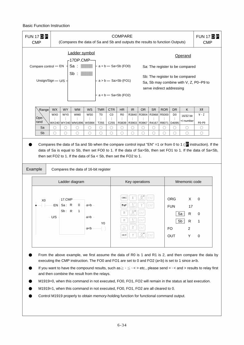
FUN 17 D P CMP
COMPARE (Compares the data of Sa and Sb and outputs the results to function Outputs)
FUN 17 D PCMP
Sa :ENCompare control
Ladder symbol
17DP.CMP
Sb :
U/S
a = b
a > b
a < b
Sa=Sb (FO0)
Sa>Sb (FO1)
Sa<Sb (FO2)
Unsign/Sign
Operand
Sa: The register to be compared
Sb: The register to be compared Sa, Sb may combine with V, Z, P0~P9 to serve indirect addressing
Range
Ope- rand
WX WY WM WS TMR CTR HR IR OR SR ROR DR K XR WX0
∣ WX240
WY0 ∣
WY240
WM0 ∣
WM1896
WS0 ∣
WS984
T0 ∣
T255
C0 ∣
C255
R0 ∣
R3839
R3840∣
R3903
R3904∣
R3967
R3968∣
R4167
R5000∣
R8071
D0 ∣
D4095
16/32 bit
+/-number
V、Z
P0~P9 Sa ○ ○ ○ ○ ○ ○ ○ ○ ○ ○ ○ ○ ○ ○ Sb ○ ○ ○ ○ ○ ○ ○ ○ ○ ○ ○ ○ ○ ○
● Compares the data of Sa and Sb when the compare control input "EN" =1 or from 0 to 1 ( P instruction). If the data of Sa is equal to Sb, then set FO0 to 1. If the data of Sa>Sb, then set FO1 to 1. If the data of Sa<Sb, then set FO2 to 1. If the data of Sa < Sb, then set the FO2 to 1.
Example Compares the data of 16-bit register
Ladder diagram Key operations Mnemonic code
X0Sa :
Sb :
R
R
0
1
17.CMP
a=b
a>b
a<bY0
U/S
EN
OUT
ORG
ORG X 0
FUN 17
Sa : R 0
Sb : R 1
FO 2
OUT Y 0
● From the above example, we first assume the data of R0 is 1 and R1 is 2, and then compare the data by
executing the CMP instruction. The FO0 and FO1 are set to 0 and FO2 (a<b) is set to 1 since a<b.
● If you want to have the compound results, such as≧、≦、< > etc., please send =、< and > results to relay first and then combine the result from the relays.
● M1919=0, when this command in not executed, FO0, FO1, FO2 will remain in the status at last execution.
● M1919=1, when this command in not executed, FO0, FO1, FO2 are all cleared to 0.
● Control M1919 properly to obtain memory-holding function for functional command output.
Basic Function Instruction
6-35
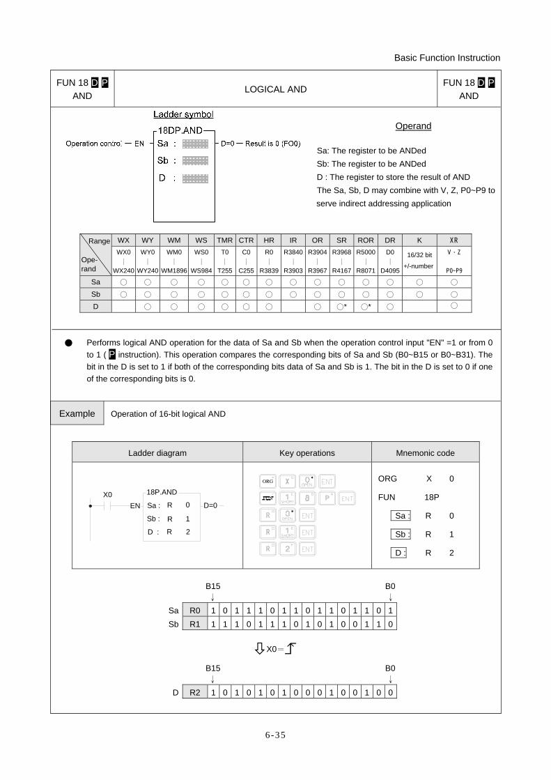
FUN 18 D P AND
LOGICAL AND FUN 18 D P
AND
Operand
Sa: The register to be ANDed Sb: The register to be ANDed D : The register to store the result of AND The Sa, Sb, D may combine with V, Z, P0~P9 to serve indirect addressing application
Range
Ope- rand
WX WY WM WS TMR CTR HR IR OR SR ROR DR K XR WX0
∣ WX240
WY0 ∣
WY240
WM0 ∣
WM1896
WS0 ∣
WS984
T0∣
T255
C0∣
C255
R0 ∣
R3839
R3840∣
R3903
R3904∣
R3967
R3968∣
R4167
R5000∣
R8071
D0 ∣
D4095
16/32 bit
+/-number
V、Z
P0~P9
Sa ○ ○ ○ ○ ○ ○ ○ ○ ○ ○ ○ ○ ○ ○ Sb ○ ○ ○ ○ ○ ○ ○ ○ ○ ○ ○ ○ ○ ○ D ○ ○ ○ ○ ○ ○ ○ ○* ○* ○ ○
● Performs logical AND operation for the data of Sa and Sb when the operation control input "EN" =1 or from 0 to 1 ( P instruction). This operation compares the corresponding bits of Sa and Sb (B0~B15 or B0~B31). The bit in the D is set to 1 if both of the corresponding bits data of Sa and Sb is 1. The bit in the D is set to 0 if one of the corresponding bits is 0.
Example Operation of 16-bit logical AND
Ladder diagram Key operations Mnemonic code
X0Sa :
Sb :
D :
R
R
R
0
1
2
18P.AND
D=0EN
ORG
ORG X 0
FUN 18P
Sa : R 0
Sb : R 1
D : R 2
B15 B0 ↓ ↓
Sa R0 1 0 1 1 1 0 1 1 0 1 1 0 1 1 0 1 Sb R1 1 1 1 0 1 1 1 0 1 0 1 0 0 1 1 0
X0=
B15 B0 ↓ ↓
D R2 1 0 1 0 1 0 1 0 0 0 1 0 0 1 0 0
Basic Function Instruction
6-36
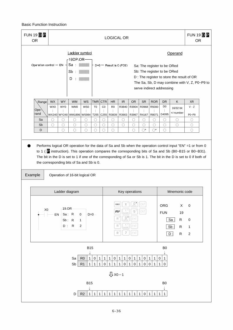
FUN 19 D P OR
LOGICAL OR FUN 19 D P
OR
Operand
Sa: The register to be ORed Sb: The register to be ORed D : The register to store the result of OR The Sa, Sb, D may combine with V, Z, P0~P9 to serve indirect addressing
Range
Ope- rand
WX WY WM WS TMR CTR HR IR OR SR ROR DR K XR WX0
∣ WX240
WY0 ∣
WY240
WM0 ∣
WM1896
WS0 ∣
WS984
T0∣
T255
C0∣
C255
R0 ∣
R3839
R3840∣
R3903
R3904∣
R3967
R3968∣
R4167
R5000∣
R8071
D0 ∣
D4095
16/32 bit
+/-number
V、Z
P0~P9
Sa ○ ○ ○ ○ ○ ○ ○ ○ ○ ○ ○ ○ ○ ○
Sb ○ ○ ○ ○ ○ ○ ○ ○ ○ ○ ○ ○ ○ ○
D ○ ○ ○ ○ ○ ○ ○ ○* ○* ○ ○
● Performs logical OR operation for the data of Sa and Sb when the operation control input "EN" =1 or from 0 to 1 ( P instruction). This operation compares the corresponding bits of Sa and Sb (B0~B15 or B0~B31). The bit in the D is set to 1 if one of the corresponding of Sa or Sb is 1. The bit in the D is set to 0 if both of the corresponding bits of Sa and Sb is 0.
Example Operation of 16-bit logical OR
Ladder diagram Key operations Mnemonic code
X0EN Sa :
Sb :
D :
R
R
R
0
1
2
19.OR
D=0
ORG
ORG X 0
FUN 19
Sa : R 0
Sb : R 1
D : R 2
B15 B0 ↓ ↓
Sa R0 1 0 1 1 1 0 1 1 0 1 1 0 1 1 0 1 Sb R1 1 1 1 0 1 1 1 0 1 0 1 0 0 1 1 0
X0=1
B15 B0 ↓ ↓
D R2 1 1 1 1 1 1 1 1 1 1 1 0 1 1 1 1
Basic Function Instruction
6-37
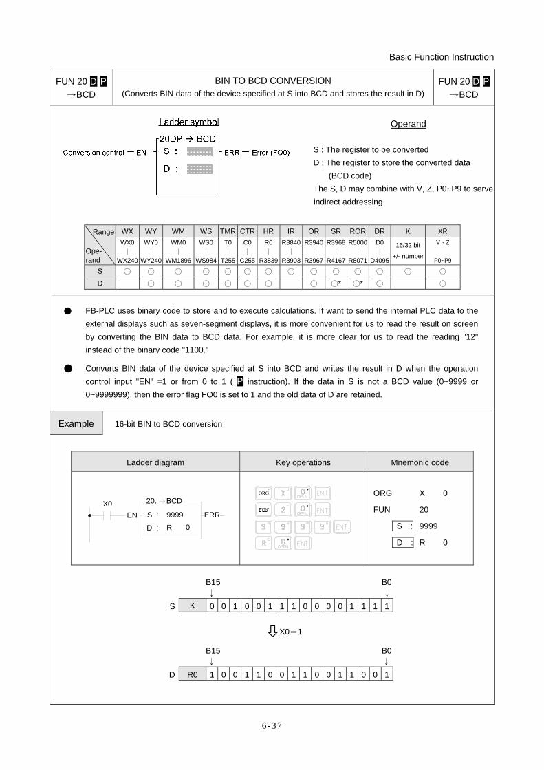
FUN 20 D P →BCD
BIN TO BCD CONVERSION (Converts BIN data of the device specified at S into BCD and stores the result in D)
FUN 20 D P→BCD
Operand
S : The register to be converted D : The register to store the converted data
(BCD code) The S, D may combine with V, Z, P0~P9 to serve indirect addressing
Range
Ope- rand
WX WY WM WS TMR CTR HR IR OR SR ROR DR K XR WX0
∣ WX240
WY0 ∣
WY240
WM0 ∣
WM1896
WS0 ∣
WS984
T0∣
T255
C0∣
C255
R0∣
R3839
R3840∣
R3903
R3940∣
R3967
R3968∣
R4167
R5000∣
R8071
D0∣
D4095
16/32 bit
+/- number
V、Z
P0~P9
S ○ ○ ○ ○ ○ ○ ○ ○ ○ ○ ○ ○ ○ ○
D ○ ○ ○ ○ ○ ○ ○ ○* ○* ○ ○
● FB-PLC uses binary code to store and to execute calculations. If want to send the internal PLC data to the external displays such as seven-segment displays, it is more convenient for us to read the result on screen by converting the BIN data to BCD data. For example, it is more clear for us to read the reading "12" instead of the binary code "1100."
● Converts BIN data of the device specified at S into BCD and writes the result in D when the operation control input "EN" =1 or from 0 to 1 ( P instruction). If the data in S is not a BCD value (0~9999 or 0~9999999), then the error flag FO0 is set to 1 and the old data of D are retained.
Example 16-bit BIN to BCD conversion
Ladder diagram Key operations Mnemonic code
X0EN S :
D : R
99990
20. BCD
ERR
ORG
ORG X 0
FUN 20
S : 9999
D : R 0
B15 B0 ↓ ↓
S K 0 0 1 0 0 1 1 1 0 0 0 0 1 1 1 1
X0=1
B15 B0 ↓ ↓
D R0 1 0 0 1 1 0 0 1 1 0 0 1 1 0 0 1
Basic Function Instruction
6-38
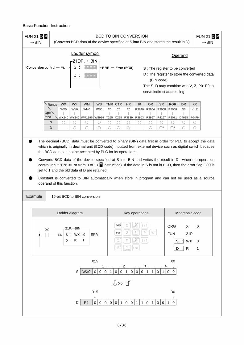
FUN 21 D P →BIN
BCD TO BIN CONVERSION (Converts BCD data of the device specified at S into BIN and stores the result in D)
FUN 21 D P→BIN
Operand
S : The register to be converted D : The register to store the converted data
(BIN code) The S, D may combine with V, Z, P0~P9 to serve indirect addressing
Range
Ope- rand
WX WY WM WS TMR CTR HR IR OR SR ROR DR XR WX0
∣ WX240
WY0 ∣
WY240
WM0 ∣
WM1896
WS0∣
WS984
T0∣
T255
C0∣
C255
R0 ∣
R3839
R3840∣
R3903
R3904∣
R3967
R3968∣
R4167
R5000 ∣
R8071
D0 ∣
D4095
V、Z
P0~P9
S ○ ○ ○ ○ ○ ○ ○ ○ ○ ○ ○ ○ ○
D ○ ○ ○ ○ ○ ○ ○ ○* ○* ○ ○
● The decimal (BCD) data must be converted to binary (BIN) data first in order for PLC to accept the data which is originally in decimal unit (BCD code) inputted from external device such as digital switch because the BCD data can not be accepted by PLC for its operations.
● Converts BCD data of the device specified at S into BIN and writes the result in D when the operation control input "EN" =1 or from 0 to 1 ( P instruction). If the data in S is not in BCD, then the error flag FO0 is set to 1 and the old data of D are retained.
● Constant is converted to BIN automatically when store in program and can not be used as a source operand of this function.
Example 16-bit BCD to BIN conversion
Ladder diagram Key operations Mnemonic code
X0S :
D : R
WX 01
21P. BIN
ERREN
ORG
ORG X 0
FUN 21P
S : WX 0
D : R 1
X15 X0 ↓ 1 2 3 4 ↓
S WX0 0 0 0 1 0 0 1 0 0 0 1 1 0 1 0 0
X0=
B15 B0 ↓ ↓
D R1 0 0 0 0 0 1 0 0 1 1 0 1 0 0 1 0