ieice technical report (reconf), january 2013
TRANSCRIPT

メッシュ接続FPGAアレーを用いた 高性能ステンシル計算機の設計と実装
2013/01/17 リコンフィギャラブルシステム研究会 FPGA計算応用 (15:15-15:40) 発表20分 + 質疑応答5分
☆小林 諒平†1 高前田(山崎) 伸也†1 †2 吉瀬 謙二†1
†1 東京工業大学 大学院情報理工学研究科
†2 日本学術振興会 特別研究員(DC1)

発表の流れ
FPGAアレーにおけるステンシル計算 ►アレー間通信の最適化
►演算ユニットのデータ処理
FPGAアレーシステムの問題点 ►クロックのばらつきの定量評価
同期機構の設計・実装
性能評価・結論
1

発表の流れ
FPGAアレーにおけるステンシル計算 ►アレー間通信の最適化
►演算ユニットのデータ処理
FPGAアレーシステムの問題点 ►クロックのばらつきの定量評価
同期機構の設計・実装
性能評価・結論
2
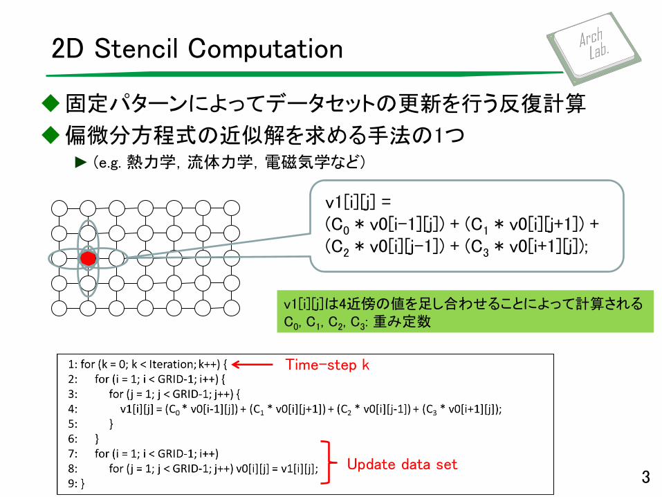
v1[i][j] = (C0 * v0[i-1][j]) + (C1 * v0[i][j+1]) + (C2 * v0[i][j-1]) + (C3 * v0[i+1][j]);
2D Stencil Computation
固定パターンによってデータセットの更新を行う反復計算
偏微分方程式の近似解を求める手法の1つ ► (e.g. 熱力学,流体力学,電磁気学など)
Time-step k
Update data set 3
v1[i][j]は4近傍の値を足し合わせることによって計算される C0, C1, C2, C3: 重み定数

FPGAアレーにおけるステンシル計算
4
:格子点 FPGA
SRAM
FPGA
SRAM
FPGA
SRAM
FPGA
SRAM
FPGA
SRAM
FPGA
SRAM
FPGA
SRAM
FPGA
SRAM
PROM PROM PROM PROM
PROM PROM PROM PROM
FPGA
SRAM
FPGA
SRAM
FPGA
SRAM
FPGA
SRAM PROM PROM PROM PROM
FPGA
SRAM
FPGA
SRAM
FPGA
SRAM
FPGA
SRAM PROM PROM PROM PROM
・データセットはFPGAの数に応じて分割され,格納される ・各FPGAは並列にステンシル計算を実行する

ScalableCore System
小容量FPGAを複数用いたタイル型アーキテクチャシミュレータ
►メニーコアプロセッサの高速シミュレータ
►このシステムのハードウェアをHPCハードウェアアクセラレータの基礎として使用
5
One FPGA node
FPGA
SRAM PROM
*Takamaeda-Yamazaki, S., (ARC 2012) (2012).

発表の流れ
FPGAアレーにおけるステンシル計算 ►アレー間通信の最適化
►演算ユニットのデータ処理
FPGAアレーシステムの問題点 ►クロックのばらつきの定量評価
同期機構の設計・実装
性能評価・結論
6
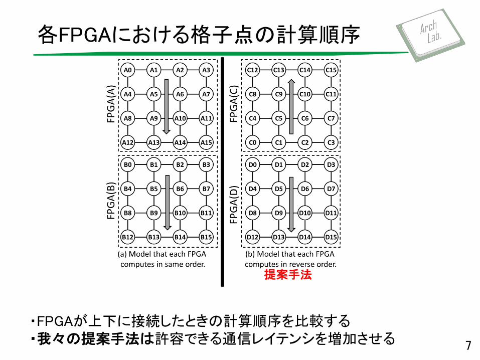
各FPGAにおける格子点の計算順序
7
提案手法
・FPGAが上下に接続したときの計算順序を比較する ・我々の提案手法は許容できる通信レイテンシを増加させる

Comparison between (a) and (b) (1/2)
8
・イテレーション : 全ての格子点を1度計算するための処理 ・簡単のため,値の更新はかかるサイクル数は1とする ・各FPGA は割り当てられた格子点16 個の値を各イテレーションごと更新する(格子点0から15への順番で更新する)
A0 A1
A4 A5
A8 A9
A12 A13
A2
A6
A10
A14
A3
A7
A11
A15
B0 B1
B4 B5
B8 B9
B12 B13
B2
B6
B10
B14
B3
B7
B11
B15
FP
GA
(A)
FP
GA
(B)
C12 C13
C8 C9
C4 C5
C0 C1
C14
C10
C6
C2
C15
C11
C7
C3
D0 D1
D4 D5
D8 D9
D12 D13
D2
D6
D10
D14
D3
D7
D11
D15
FP
GA
(C)
FP
GA
(D)
vs
(a) (b) Proposed method

Comparison between (a) and (b) (2/2)
9
A1 A0 A2 A3 A4 A5 A6 A7 A8 A9 A10 A11 A12 A13 A14 A15
B1 B0 B2 B3 B4 B5 B6 B7 B8 B9 B10 B11 B12 B13 B14 B15 B0
A0
0 16
A1
B1
…
First Iteration end A0 A1
A4 A5
A8 A9
A12 A13
A2
A6
A10
A14
A3
A7
A11
A15
B0 B1
B4 B5
B8 B9
B12 B13
B2
B6
B10
B14
B3
B7
B11
B15
FP
GA
(A)
FP
GA
(B)
C12 C13
C8 C9
C4 C5
C0 C1
C14
C10
C6
C2
C15
C11
C7
C3
D0 D1
D4 D5
D8 D9
D12 D13
D2
D6
D10
D14
D3
D7
D11
D15
FP
GA
(C)
FP
GA
(D)
(a)
(b)
Proposed method
C1 C0 C2 C3 C4 C5 C6 C7 C8 C9 C10 C11 C12 C13 C14 C15
D1 D0 D2 D3 D4 D5 D6 D7 D8 D9 D10 D11 D12 D13 D14 D15 D0
C0
0 16
C1
D1
…
First Iteration end

Comparison between (a) and (b) (2/2)
10
C12 C13
C8 C9
C4 C5
C0 C1
C14
C10
C6
C2
C15
C11
C7
C3
D0 D1
D4 D5
D8 D9
D12 D13
D2
D6
D10
D14
D3
D7
D11
D15
FP
GA
(C)
FP
GA
(D)
(b)
A1 A0 A2 A3 A4 A5 A6 A7 A8 A9 A10 A11 A12 A13 A14 A15
B1 B0 B2 B3 B4 B5 B6 B7 B8 B9 B10 B11 B12 B13 B14 B15 B0
A0
0 16
A1
B1
…
First Iteration end A0 A1
A4 A5
A8 A9
A12 A13
A2
A6
A10
A14
A3
A7
A11
A15
B0 B1
B4 B5
B8 B9
B12 B13
B2
B6
B10
B14
B3
B7
B11
B15
FP
GA
(A)
FP
GA
(B)
(a)
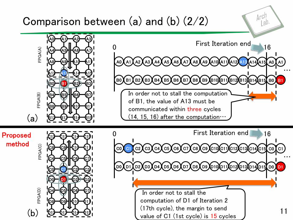
In order not to stall the computation of B1, the value of A13 must be communicated within three cycles (14, 15, 16) after the computation…
Proposed method
C1 C0 C2 C3 C4 C5 C6 C7 C8 C9 C10 C11 C12 C13 C14 C15
D1 D0 D2 D3 D4 D5 D6 D7 D8 D9 D10 D11 D12 D13 D14 D15 D0
C0
0 16
C1
D1
…
First Iteration end
Comparison between (a) and (b) (2/2)
11
A1 A0 A2 A3 A4 A5 A6 A7 A8 A9 A10 A11 A12 A13 A14 A15
B1 B0 B2 B3 B4 B5 B6 B7 B8 B9 B10 B11 B12 B13 B14 B15 B0
A0
0 16
A1
B1
…
First Iteration end A0 A1
A4 A5
A8 A9
A12 A13
A2
A6
A10
A14
A3
A7
A11
A15
B0 B1
B4 B5
B8 B9
B12 B13
B2
B6
B10
B14
B3
B7
B11
B15
FP
GA
(A)
FP
GA
(B)
C12 C13
C8 C9
C4 C5
C0 C1
C14
C10
C6
C2
C15
C11
C7
C3
D0 D1
D4 D5
D8 D9
D12 D13
D2
D6
D10
D14
D3
D7
D11
D15
FP
GA
(C)
FP
GA
(D)
C1 C0 C2 C3 C4 C5 C6 C7 C8 C9 C10 C11 C12 C13 C14 C15
D1 D0 D2 D3 D4 D5 D6 D7 D8 D9 D10 D11 D12 D13 D14 D15 D0
C0
0 16
C1
D1
…
First Iteration end
(a)
(b)
Proposed method
In order not to stall the computation of B1, the value of A13 must be communicated within three cycles (14, 15, 16) after the computation…
In order not to stall the computation of D1 of Iteration 2 (17th cycle), the margin to send value of C1 (1st cycle) is 15 cycles

Comparison between (a) and (b) (N×M grid-points)
12
FP
GA
FP
GA
If the N×M grid-points are assigned to a single FPGA, every shared value must be communicated within N–1cycles
N
M
FP
GA
FP
GA
M
N
… …
Iteration end
N-1 cycles
… …
Iteration end
N×M-1 cycles
If the N×M grid-points are assigned to a single FPGA, every shared value must be communicated within N×M–1cycles
(a)
(b)
Proposed method

Computing Order Applied Proposed Method
13
:computation order
この提案手法により約1イテレーションの許容できる通信レイテンシを確保 格子点の数が増加するほど,許容できる通信レイテンシはスケールする

発表の流れ
FPGAアレーにおけるステンシル計算 ►アレー間通信の最適化
►演算ユニットのデータ処理
FPGAアレーシステムの問題点 ►クロックのばらつきの定量評価
同期機構の設計・実装
性能評価・結論
14

System Architecture
15
Ser/Des Ser/Des
Clock
Reset
FPGASpartan-6
Configura onROMXCF04S
West East
mux mux mux mux mux mux mux mux
mux8
MADD MADD MADD MADD MADD MADD MADD MADD
mux2
Ser/Des
Ser/Des
North
South
Sync
0 1 2 3 4 5 6 7 0 1 2 3 4 5 6 7
0 1 2 3 4 5 6 7 W E
Memory unit (BlockRAMs)
Computation unit (Multiply and Adder)

Relationship between The Data Subset and BlockRAM(Memory unit)
16
BlockRAM: low-latency SRAM which each FPGA has.
The data set which assigned to each FPGA is split in the vertical direction, and is stored in each BlockRAM (0~7)
If the data set of 64×128 is assigned to one FPGA, the split data set (8×128) is stored in each BlockRAM (0~7).
FPGA array 4×4 (Data is assigned)
BlockRAMs

Relationship between MADD and BlockRAM(Memory unit)
17
・The data set stored in each BlockRAM is computed by each MADD. ・Each MADD performs the computation in parallel. ・The computed data is stored in BlockRAM.

MADD Architecture(Computation unit)
MADD ►Multiply: seven pipeline stages
►Adder: seven pipeline stages
►Both multiply and adder are single precision floating-point unit which conforms to IEEE 754.
18

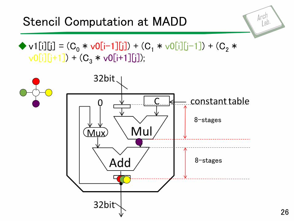
Stencil Computation at MADD
v1[i][j] = (C0 * v0[i-1][j]) + (C1 * v0[i][j-1]) + (C2 * v0[i][j+1]) + (C3 * v0[i+1][j]);
19
8-stages
8-stages

Stencil Computation at MADD
v1[i][j] = (C0 * v0[i-1][j]) + (C1 * v0[i][j-1]) + (C2 * v0[i][j+1]) + (C3 * v0[i+1][j]);
20
8-stages
8-stages
C0

Stencil Computation at MADD
v1[i][j] = (C0 * v0[i-1][j]) + (C1 * v0[i][j-1]) + (C2 * v0[i][j+1]) + (C3 * v0[i+1][j]);
21
8-stages
8-stages
Take 8 cycles
C1

Stencil Computation at MADD
v1[i][j] = (C0 * v0[i-1][j]) + (C1 * v0[i][j-1]) + (C2 * v0[i][j+1]) + (C3 * v0[i+1][j]);
22
8-stages
8-stages
C1

Stencil Computation at MADD
v1[i][j] = (C0 * v0[i-1][j]) + (C1 * v0[i][j-1]) + (C2 * v0[i][j+1]) + (C3 * v0[i+1][j]);
23
8-stages
8-stages
Take 8 cycles
Take 8 cycles
C2

Stencil Computation at MADD
v1[i][j] = (C0 * v0[i-1][j]) + (C1 * v0[i][j-1]) + (C2 * v0[i][j+1]) + (C3 * v0[i+1][j]);
24
8-stages
8-stages
C2

Stencil Computation at MADD
v1[i][j] = (C0 * v0[i-1][j]) + (C1 * v0[i][j-1]) + (C2 * v0[i][j+1]) + (C3 * v0[i+1][j]);
25
8-stages
8-stages
C3
Stencil Computation at MADD
v1[i][j] = (C0 * v0[i-1][j]) + (C1 * v0[i][j-1]) + (C2 * v0[i][j+1]) + (C3 * v0[i+1][j]);
26
8-stages
8-stages

Stencil Computation at MADD
v1[i][j] = (C0 * v0[i-1][j]) + (C1 * v0[i][j-1]) + (C2 * v0[i][j+1]) + (C3 * v0[i+1][j]);
27
8-stages
8-stages
V1[i][j]

MADD Pipeline Operation(Computation unit)
The computation of grid-points 11~18
28
Input2(adder)
Input1(adder)
8-stages
8-stages
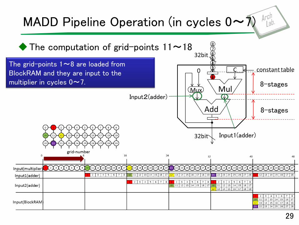
MADD Pipeline Operation (in cycles 0〜7)
The computation of grid-points 11~18
29
The grid-points 1~8 are loaded from BlockRAM and they are input to the multiplier in cycles 0~7.
1 2 3 4 5 6 7 8
Input2(adder)
Input1(adder)
8-stages
8-stages
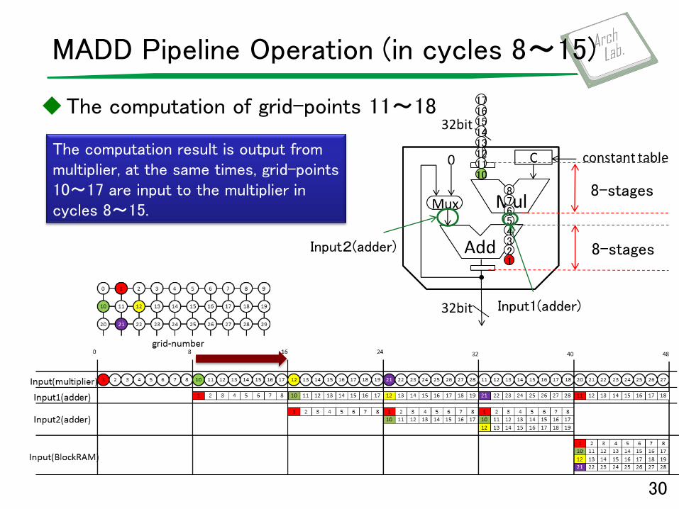
MADD Pipeline Operation (in cycles 8〜15)
The computation of grid-points 11~18
30
The computation result is output from multiplier, at the same times, grid-points 10~17 are input to the multiplier in cycles 8~15.
10 11 12 13 14 15 16 17
1 2 3 4 5 6 7 8
Input2(adder)
Input1(adder)
8-stages
8-stages
Input2(adder)
Input1(adder)
8-stages
8-stages
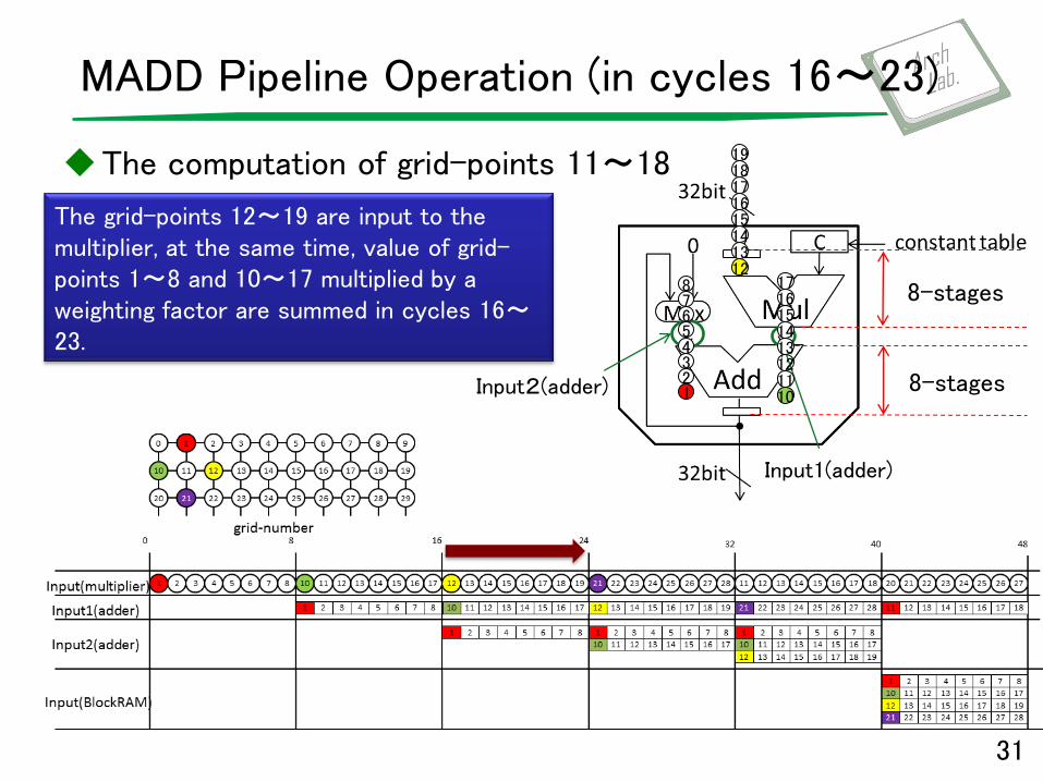
MADD Pipeline Operation (in cycles 16〜23)
The computation of grid-points 11~18
31
The grid-points 12~19 are input to the multiplier, at the same time, value of grid-points 1〜8 and 10~17 multiplied by a weighting factor are summed in cycles 16~23.
12 13 14 15 16 17 18 19
1 2 3 4 5 6 7 8
10 11 12 13 14 15 16 17
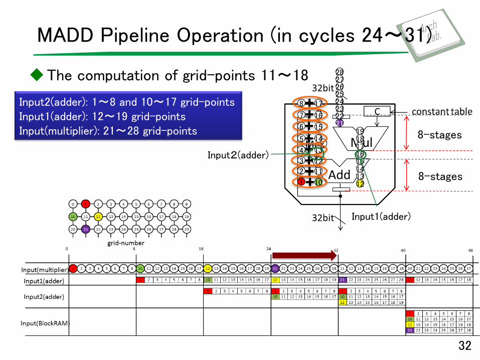
MADD Pipeline Operation (in cycles 24〜31)
The computation of grid-points 11~18
32
1
2
3
4
5
6
7
8
10
11
12
13
14
15
16
17
12 13 14 15 16 17 18 19
21 22 23 24 25 26 27 28
Input2(adder): 1~8 and 10~17 grid-points Input1(adder): 12~19 grid-points Input(multiplier): 21~28 grid-points
Input2(adder)
Input1(adder)
8-stages
8-stages

MADD Pipeline Operation (in cycles 32〜39)
The computation of grid-points 11~18
33
1
2
3
4
5
6
7
8
10
11
12
13
14
15
16
17
12
13
14
15
16
17
18
19
21 22 23 24 25 26 27 28
11 12 13 14 15 16 17 18
Input2(adder): 1~8, 10~17 and 12~19 grid-points Input1(adder): 21~28 grid-points Input(multiplier): 11~18 grid-points
Input2(adder)
Input1(adder)
8-stages
8-stages

Input2(adder)
Input1(adder)
8-stages
8-stages
MADD Pipeline Operation (in cycles 40〜48)
The computation of grid-points 11~18
34
1 2
3
4 5
6
7
8
10
11
12
13
14
15
16
17
12
13
14
15
16
17
18
19
21
22
23
24
25
26 27
28
The computation results that data of up, down, left and right gird-points are multiplied by a weighting factor and summed are output in cycles 40~48.
11 12 13 14 15 16 17 18
20 21 22 23 24 25 26 27

MADD Pipeline Operation(Computation unit)
The filing rate of the pipeline: (N-8/N)×100% (N is
cycles which taken this computation.)
► Achievement of high computation performance and the small circuit area
► This scheduling is valid only when width of computed grid is equal to the pipeline stages of multiplier and adder.
35

発表の流れ
FPGAアレーにおけるステンシル計算 ►アレー間通信の最適化
►演算ユニットのデータ処理
FPGAアレーシステムの問題点 ►クロックのばらつきの定量評価
同期機構の設計・実装
性能評価・結論
36

このFPGAアレーシステムはグローバルクロックを有していない!
►各ノードは固有のクロックドメインを持っている
クロック周期のずれを定量的に評価
計算機が長時間,安定して動作するための機構を設計・実装
FPGAアレーシステムの問題点
37
ノード数を増加させた時に,計算機の不具合を発見! 各FPGAノードのクロック周期のばらつきが原因??
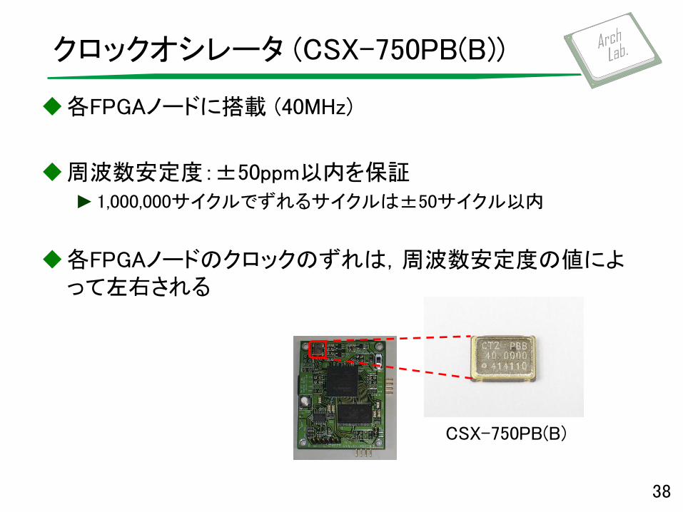
クロックオシレータ (CSX-750PB(B))
各FPGAノードに搭載 (40MHz)
周波数安定度:±50ppm以内を保証 ►1,000,000サイクルでずれるサイクルは±50サイクル以内
各FPGAノードのクロックのずれは,周波数安定度の値によって左右される
38
CSX-750PB(B)

クロックのずれの評価(1/3)
ScalableCoreシステムを利用 (8×8構成)
計測時間を変化させてクロックのずれを測定
39
Power Supply
USB Port
FPGA
SRAM
FPGA
SRAM
FPGA
SRAM
FPGA
SRAM
FPGA
SRAM
FPGA
SRAM
FPGA
SRAM
FPGA
SRAM
PROM PROM PROM PROM
PROM PROM PROM PROM
Display
FPGA
SRAM
FPGA
SRAM PROM
PROM
FPGA
SRAM
FPGA
SRAM PROM
PROM
FPGA
SRAM
FPGA
SRAM
FPGA
SRAM
FPGA
SRAM PROM PROM PROM PROM
FPGA
SRAM PROM
FPGA
SRAM PROM

クロックのずれの評価(2/3)
X軸,Y軸:各FPGAノードの座標
Z軸1,000,000サイクルあたりのクロックのずれ(ppm)
40
x=1
x=2
x=3
x=4
x=5
x=6
x=7x=8
0.00
5.00
10.00
15.00
20.00
25.00
12
34
56
78
cyclevariea
on/M
ccycle
x=1
x=2
x=3
x=4
x=5
x=6
x=7
x=8
20sec x=1
x=2
x=3
x=4
x=5
x=6
x=7x=8
-5.00
0.00
5.00
10.00
15.00
20.00
25.00
12
34
56
78
cyclevariea
on/M
ccycle
x=1
x=2
x=3
x=4
x=5
x=6
x=7
x=8
80sec x=1
x=2
x=3
x=4
x=5
x=6
x=7x=8
-5.00
0.00
5.00
10.00
15.00
20.00
25.00
12
34
56
78
cyclevariea
on/M
ccycle
x=1
x=2
x=3
x=4
x=5
x=6
x=7
x=8
320sec
測定時間:20sec 最悪のずれ:20.5ppm (x=3, y=5) クロックのばらつきの標準偏差:4.73
測定時間:80sec 最悪のずれ:20.5ppm (x=3, y=5) クロックのばらつきの標準偏差:4.73
測定時間:80sec 最悪のずれ:20.7ppm (x=3, y=5) クロックのばらつきの標準偏差:4.79
・周波数安定度±50ppmが保証されていることを確認

クロックのずれの評価(3/3)
41
・クロックのずれは,時間には依存しないことを確認 →時間軸上ではほぼ変化しないクロックのずれを考慮したシステム設計が必要
x=1
x=2
x=3
x=4
x=5
x=6
x=7
x=8
-4.00
-3.50
-3.00
-2.50
-2.00
-1.50
-1.00
-0.50
0.00
0.50
1.00
1.50
12
34
56
78
cyclevariea
on/M
ccycle
x=1
x=2
x=3
x=4
x=5
x=6
x=7
x=8
320secのクロックのずれを20secのクロックのずれで割ったグラフ
測定時間[sec] 最悪のずれ[ppm]
ずれの標準偏差
20 20.47(x=3, y=5) 4.73
40 20.47(x=3, y=5) 4.68
80 20.47(x=3, y=5) 4.73
160 20.59(x=3, y=5) 4.77
320 20.66(x=3, y=5) 4.79
各測定時間における最悪のずれとずれの標準偏差

発表の流れ
FPGAアレーにおけるステンシル計算 ►アレー間通信の最適化
►演算ユニットのデータ処理
FPGAアレーシステムの問題点 ►クロックのばらつきの定量評価
同期機構の設計・実装
性能評価・結論
42

同期機構の設計
FPGAノード(A)をMasterノードと定義
各FPGAノードはMasterノードからα +β の周期で送信される信号に同期して計算を実行
同期信号を受信するまで,Masterノード以外のノードは計算をストール
43
α A
B
C
D
stall
synchronize synchronize
α α
stall stall
β β β α :1 イテレーション間におけるステンシル計算に要するサイクル β :各FPGAノードのクロックのずれを吸収するマージン

同期機構の実装
各FPGAノードはMasterノードからα +β の周期で送信される信号に同期して計算を実行
同期信号を受信するまで,Masterノード以外のノードは計算をストール
信号を受信したFPGAノードは数サイクル待ってから,左方向と下方向に同期信号を送信し,計算を再開
44
D
B
C
A master
A
B
for anti-chattering C
D
for anti-chattering
α β
α β

同期機構の動作検証(100ノード)
45 Coming soon!!

発表の流れ
FPGAアレーにおけるステンシル計算 ►アレー間通信の最適化
►演算ユニットのデータ処理
FPGAアレーシステムの問題点 ►クロックのばらつきの定量評価
同期機構の設計・実装
性能評価・結論
46

Environment (Performance of Single FPGA Node)
FPGA:Xilinx Spartan-6 XC6SLX16
► BlockRAM: 64KB
Design tool: Xilinx ISE webpack 13.3
Hardware description language: Verilog HDL
Implementation of MADD:IP core generated by Xilinx core-generator
► Implementing single MADD expends four pieces of 32 DSP-blocks which a Spartan-6 FPGA has.
◇Therefore, the number of MADD to be able to be implemented in single FPGA is eight
47 ScalableCore board
SRAM is not used.
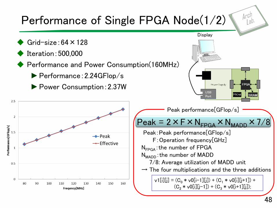
Performance of Single FPGA Node(1/2)
Grid-size:64×128
Iteration:500,000
Performance and Power Consumption(160MHz)
►Performance:2.24GFlop/s
►Power Consumption:2.37W
48
Peak = 2×F×NFPGA×NMADD×7/8 Peak:Peak performance[GFlop/s] F:Operation frequency[GHz] NFPGA:the number of FPGA NMADD:the number of MADD 7/8: Average utilization of MADD unit → The four multiplications and the three additions
Peak performance[GFlop/s]
v1[i][j] = (C0 * v0[i-1][j]) + (C1 * v0[i][j+1]) + (C2 * v0[i][j-1]) + (C3 * v0[i+1][j]);
Performance of Single FPGA Node(2/2)
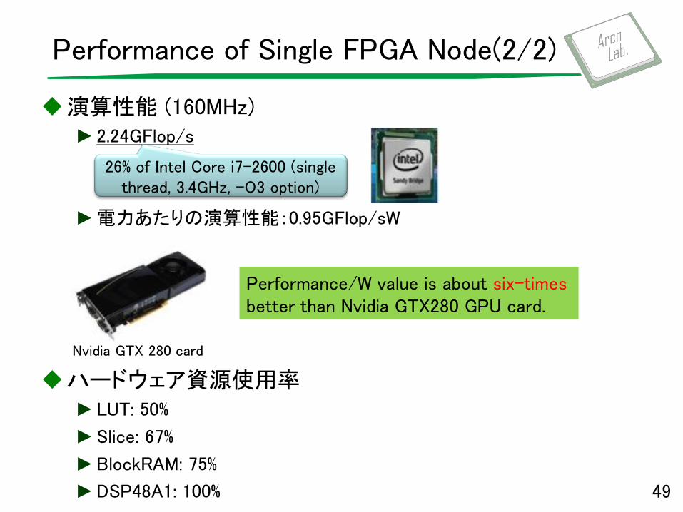
演算性能 (160MHz) ►2.24GFlop/s
►電力あたりの演算性能:0.95GFlop/sW
ハードウェア資源使用率 ►LUT: 50%
►Slice: 67%
►BlockRAM: 75%
►DSP48A1: 100% 49
26% of Intel Core i7-2600 (single thread, 3.4GHz, -O3 option)
Nvidia GTX 280 card
Performance/W value is about six-times better than Nvidia GTX280 GPU card.

Conclusion
クロックのずれを定量的に評価 ►クロックのずれは動作時間に依存しない
設計および実装 ►各FPGAノードの位置情報を取得する回路を実装
►各FPGAが同期する機構を実装
►100ノードでの動作を確認
性能評価 (One-FPGA node) ►動作周波数 160MHz (no communication)
►実行性能 2.24GFlop/s. 消費電力 2.37W.
►ハードウェア資源使用率 : Slices 67%
今後の課題 ►FPGAアレーの性能評価
►低電力に向けた実装
50