infineon-tle8209-4sa-ds-v01_02-en.pdf
TRANSCRIPT

TLE8209-4SASPI Programmable H-Br idge
Data Sheet, Rev. 1.2, July 2013
Automot ive Power

Data Sheet 2 Rev. 1.2, 2013-07-13
TLE8209-4SA
Table of Contents
1 Overview . . . . . . . . . . . . . . . . . . . . . . . . . . . . . . . . . . . . . . . . . . . . . . . . . . . . . . . . . . . . . . . . . . . . . . . 3
2 Pin Configuration . . . . . . . . . . . . . . . . . . . . . . . . . . . . . . . . . . . . . . . . . . . . . . . . . . . . . . . . . . . . . . . . 42.1 Pin Assignment . . . . . . . . . . . . . . . . . . . . . . . . . . . . . . . . . . . . . . . . . . . . . . . . . . . . . . . . . . . . . . . . . . . 42.2 Pin Definitions and Functions . . . . . . . . . . . . . . . . . . . . . . . . . . . . . . . . . . . . . . . . . . . . . . . . . . . . . . . . 42.3 Terms . . . . . . . . . . . . . . . . . . . . . . . . . . . . . . . . . . . . . . . . . . . . . . . . . . . . . . . . . . . . . . . . . . . . . . . . . . 5
3 Block Diagram . . . . . . . . . . . . . . . . . . . . . . . . . . . . . . . . . . . . . . . . . . . . . . . . . . . . . . . . . . . . . . . . . . . 6
4 General Product Characteristics . . . . . . . . . . . . . . . . . . . . . . . . . . . . . . . . . . . . . . . . . . . . . . . . . . . . 74.1 Absolute Maximum Ratings . . . . . . . . . . . . . . . . . . . . . . . . . . . . . . . . . . . . . . . . . . . . . . . . . . . . . . . . . 74.2 Operating Range . . . . . . . . . . . . . . . . . . . . . . . . . . . . . . . . . . . . . . . . . . . . . . . . . . . . . . . . . . . . . . . . . 84.3 Thermal Resistance . . . . . . . . . . . . . . . . . . . . . . . . . . . . . . . . . . . . . . . . . . . . . . . . . . . . . . . . . . . . . . . 8
5 Power Supply . . . . . . . . . . . . . . . . . . . . . . . . . . . . . . . . . . . . . . . . . . . . . . . . . . . . . . . . . . . . . . . . . . . 95.1 Basic Supply Characteristics . . . . . . . . . . . . . . . . . . . . . . . . . . . . . . . . . . . . . . . . . . . . . . . . . . . . . . . . 95.2 VDD Monitoring . . . . . . . . . . . . . . . . . . . . . . . . . . . . . . . . . . . . . . . . . . . . . . . . . . . . . . . . . . . . . . . . . . 95.3 VDDIO - Digital Output Supply and Diagnostic Mode Selection . . . . . . . . . . . . . . . . . . . . . . . . . . . . . 105.4 Electrical Characteristics Power Supply and VDD-Monitoring . . . . . . . . . . . . . . . . . . . . . . . . . . . . . . . 11
6 Logic Inputs and Outputs . . . . . . . . . . . . . . . . . . . . . . . . . . . . . . . . . . . . . . . . . . . . . . . . . . . . . . . . 12
7 Power Stages . . . . . . . . . . . . . . . . . . . . . . . . . . . . . . . . . . . . . . . . . . . . . . . . . . . . . . . . . . . . . . . . . . 147.1 Parallel or SPI Control . . . . . . . . . . . . . . . . . . . . . . . . . . . . . . . . . . . . . . . . . . . . . . . . . . . . . . . . . . . . 147.2 H-Bridge or Single Switch Usage . . . . . . . . . . . . . . . . . . . . . . . . . . . . . . . . . . . . . . . . . . . . . . . . . . . . 147.3 Electrical Characteristics Power Stages . . . . . . . . . . . . . . . . . . . . . . . . . . . . . . . . . . . . . . . . . . . . . . . 15
8 Protection and Monitoring . . . . . . . . . . . . . . . . . . . . . . . . . . . . . . . . . . . . . . . . . . . . . . . . . . . . . . . . 188.1 Diagnosis in Status Flag Mode . . . . . . . . . . . . . . . . . . . . . . . . . . . . . . . . . . . . . . . . . . . . . . . . . . . . . . 188.2 Current Limitation . . . . . . . . . . . . . . . . . . . . . . . . . . . . . . . . . . . . . . . . . . . . . . . . . . . . . . . . . . . . . . . . 188.3 Temperature Dependent Current Reduction . . . . . . . . . . . . . . . . . . . . . . . . . . . . . . . . . . . . . . . . . . . 198.4 Short Circuit to Ground . . . . . . . . . . . . . . . . . . . . . . . . . . . . . . . . . . . . . . . . . . . . . . . . . . . . . . . . . . . . 198.5 Short Circuit to Battery . . . . . . . . . . . . . . . . . . . . . . . . . . . . . . . . . . . . . . . . . . . . . . . . . . . . . . . . . . . . 208.6 Short Circuit across the Load . . . . . . . . . . . . . . . . . . . . . . . . . . . . . . . . . . . . . . . . . . . . . . . . . . . . . . . 208.7 Overtemperature . . . . . . . . . . . . . . . . . . . . . . . . . . . . . . . . . . . . . . . . . . . . . . . . . . . . . . . . . . . . . . . . . 208.8 Undervoltage Shut-Down . . . . . . . . . . . . . . . . . . . . . . . . . . . . . . . . . . . . . . . . . . . . . . . . . . . . . . . . . . 208.9 Open Load Diagnosis . . . . . . . . . . . . . . . . . . . . . . . . . . . . . . . . . . . . . . . . . . . . . . . . . . . . . . . . . . . . . 208.10 Electrical Characteristics . . . . . . . . . . . . . . . . . . . . . . . . . . . . . . . . . . . . . . . . . . . . . . . . . . . . . . . . . . 22
9 SPI Interface . . . . . . . . . . . . . . . . . . . . . . . . . . . . . . . . . . . . . . . . . . . . . . . . . . . . . . . . . . . . . . . . . . . 249.1 General SPI Characteristics . . . . . . . . . . . . . . . . . . . . . . . . . . . . . . . . . . . . . . . . . . . . . . . . . . . . . . . . 249.2 SPI Communication . . . . . . . . . . . . . . . . . . . . . . . . . . . . . . . . . . . . . . . . . . . . . . . . . . . . . . . . . . . . . . 259.3 Electrical Characteristics SPI . . . . . . . . . . . . . . . . . . . . . . . . . . . . . . . . . . . . . . . . . . . . . . . . . . . . . . . 33
10 Application Information . . . . . . . . . . . . . . . . . . . . . . . . . . . . . . . . . . . . . . . . . . . . . . . . . . . . . . . . . . 34
11 Package Outlines TLE8209-4SA . . . . . . . . . . . . . . . . . . . . . . . . . . . . . . . . . . . . . . . . . . . . . . . . . . . 36
12 Revision History . . . . . . . . . . . . . . . . . . . . . . . . . . . . . . . . . . . . . . . . . . . . . . . . . . . . . . . . . . . . . . . . 37
Table of Contents

Type Package Body Width MarkingTLE8209-4SA PG-DSO-20-65 430 mil TLE8209-4SA
PG-DSO-20-65
Data Sheet 3 Rev. 1.2, 2013-07-13
SPI Programmable H-Bridge
TLE8209-4SA
1 Overview
Features• Programmable current limitation from 1.8 to 10.6 A typ.• Full path RDSon of 240 mΩ (typ. at Tj=25°C)• Operating battery supply voltage 4.5 V to 28 V• Operating logic supply voltage 4.4 to 5.25 V• Low standby current (8 µA typ.)• Logic inputs TTL/CMOS-compatible• All I/O pins overvoltage tolerant up to 18 V• Enable and disable input• Short circuit and overtemperature protection• VS undervoltage shutdown• VDD over and undervoltage monitoring• Open load detection in off condition• Temperature dependent current reduction• Extensive diagnosis capabilities via SPI interface• Status Flag for basic diagnosis without SPI• Configurable as H-bridge or two independent half bridges• Control of power stages by parallel inputs or via SPI• Output switching frequency up to 11 kHz• Slewrate programmable through SPI• Excellent EMC performance• AEC qualified• Green product (RoHS compliant)
Functional DescriptionThe TLE8209-4SA is a SPI programmable H-bridge, designed for the control of DC motors in safety criticalautomotive applications. It features four selectable current ranges, two selectable slew rate settings and extensivediagnosis via SPI. The device monitors the digital supply voltage VDD and shuts down the output stages in case ofVDD over- or undervoltage, thus providing a safe switch off path in case of malfunction of the digital control circuitry.In order to reduce power dissipation in extreme thermal conditions the current limitation threshold is reducedlinearly for junction temperatures over 165°C. A thermal warning bit is set in the SPI. The two half bridges can also be used independently to drive two separate loads like solenoids or unidirectionalDC motors.

TLE8209-4SA
Pin Configuration
Data Sheet 4 Rev. 1.2, 2013-07-13
2 Pin Configuration
2.1 Pin Assignment
Figure 1 Pinout TLE8209-4SA
2.2 Pin Definitions and Functions
Pin Symbol Function in SPI Mode Function in Status Flag Mode1 GND Ground Ground2 SO SPI Serial Data Out no function - connect to GND3 VDDIO Supply Voltage for Logic Output Buffer Switches to SF-mode if connected to GND4 SS/SF Slave Select (low active) Status Flag (low active)5 CP Pin for external Charge Pump Capacitor Pin for external Charge Pump Capacitor6 VS Battery Supply Voltage, has to be connected to
pin 15Battery Supply Voltage, has to be connected to pin 15
7 IN1 Input 1 Input 18 OUT1 Output 1 Output 19 DIS Disable Disable10 GND Ground Ground11 GND Ground Ground12 ABE Bidirectional Enable Pin Bidirectional Enable Pin13 OUT2 Output 2 Output 214 IN2 Input 2 Input 215 VS Input battery supply voltage, has to be
connected to pin 6Input battery supply voltage, has to be connected to pin 6
16 SI SPI Serial Data Input no function - connect to GND
1
2
3
4
5
6
7
8
9
10
20
19
18
17
16
15
14
13
12
11
GNDABE
OUT2
IN2
GND
VDD
CP
OUT1
VS
SCK
VDDIO
GND
GND GND
VS
SO
SI
IN1
DIS ABE
SS/SF
21GND
Data Sheet 5 Rev. 1.2, 2013-07-13
TLE8209-4SA
Pin Configuration
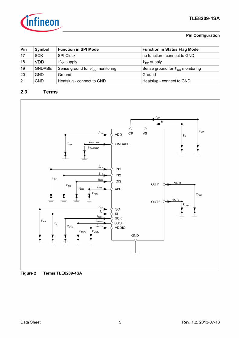
2.3 Terms
Figure 2 Terms TLE8209-4SA
17 SCK SPI Clock no function - connect to GND18 VDD VDD supply VDD supply19 GNDABE Sense ground for VDD monitoring Sense ground for VDD monitoring20 GND Ground Ground21 GND Heatslug - connect to GND Heatslug - connect to GND
Pin Symbol Function in SPI Mode Function in Status Flag Mode
VDD
ABE
GNDABE
SOSI
DIS
SCKSS/SFVDDIO
IN1
IN2
OUT1
GND
VS
OUT2
VDDIO
ISS/SF
ISCK
ISI
ISO
IDIS
IIN 2
IIN 1
IGNDABE
IABE
IDD
IDDIO
VSS/SF
VSCKVSI
VSO
VDIS
VIN2
VIN1
VGNDABE
VABE
VDD
IOUT1
IOUT2
VOUT2
VOUT1
IS
VSCP
VCP
ICP

TLE8209-4SA
Block Diagram
Data Sheet 6 Rev. 1.2, 2013-07-13
3 Block Diagram
Figure 3 Block Diagram TLE8209-4SA
VDD-Monitoring
VDD
ABE
GNDABE
SO
SI
DIS
SCK
SS/SF
VDDIO
IN1
IN2
OUT1
GND
VS
OUT2
Logic
SPI/Flag
Gate Control
VSUndervoltage
Diagnostics
internal Supply
CP

Data Sheet 7 Rev. 1.2, 2013-07-13
TLE8209-4SA
General Product Characteristics
4 General Product Characteristics
4.1 Absolute Maximum Ratings
Note: Stresses above the ones listed here may cause permanent damage to the device. Exposure to absolute maximum rating conditions for extended periods may affect device reliability.
Note: Integrated protection functions are designed to prevent IC destruction under fault conditions described in the data sheet. Fault conditions are considered as “outside” normal operating range. Protection functions are not designed for continuous repetitive operation.
Absolute Maximum Ratings 1)
Tj = -40 ⋅C to 150 ⋅C; all voltages with respect to ground, positive current flowing into pin(unless otherwise specified)
1) Not subject to production test, specified by design.
Pos. Parameter Symbol Limit Values Unit Test Conditions / CommentMin. Max.
4.1.1 Junction temperature Tj -40150
150175
°C –100h cumulative
4.1.2 Storage temperature Ts -55 150 °C –4.1.3 Ambient temperature Ta -40 125 °C –4.1.4 Battery supply voltage VS -0.5 40 V Static destruction proof
-2 40 V Dynamic destruction prooft < 0.5 s (single pulse,Tjstart < 85 °C)
4.1.5 Logic supply voltage VDD -0.5 18 V –4.1.6 Supply for logic out VDDIO -0.5 18 V –4.1.7 Voltage at logic pins
ABE, IN1, IN2, DIS, SCK, SS/SF, SI
VIN -0.5 18 V –
4.1.8 Voltage at SO VSO -0.5 VDDIO+0.3
V –
4.1.9 Voltage at CP VCP VS-0.3 VS+5.0 V 0V < VS < 40V4.1.10 Voltage at GNDABE VGNDABE VGND-0.3 VGND+0.3 VESD Susceptibility4.1.11 ESD Resistivity to GND VESD -2 2 kV HBM2)
2) ESD susceptibility HBM according to EIA/JESD22-A114-B (1.5kΩ, 100pF)
4.1.12 -8 8 kV HBM2), Pins OUT1 and OUT24.1.13 -500 500 V CDM3)
3) ESD susceptibility, Charged Device Model “CDM” EIA/JESD22-C101
4.1.14 -750 750 V CDM3), Pins 1, 10, 11, 20

TLE8209-4SA
General Product Characteristics
Data Sheet 8 Rev. 1.2, 2013-07-13
4.2 Operating Range
Note: Within the operating range the IC operates as described in the circuit description. The electrical characteristics are specified within the conditions given in the related electrical characteristics table.
4.3 Thermal Resistance
Pos. Parameter Symbol Limit Values Unit RemarkMin. Max.
4.2.1 VS supply voltage range VS 4.5 28 V –4.2.2 VDD supply voltage VDD 4.4 5.25 V –4.2.3 VDDIO supply voltage VDDIO 0 5.5 V –4.2.4 PWM frequency f – 11 kHz –4.2.5 Junction temperature TJ -40 150 °C –
Pos. Parameter Symbol Limit Values Unit RemarkMin. Typ. Max.
4.3.6 Junction to Case1)
1) Not subject to production test, specified by design.
RthJC – – 1.6 K/W –4.3.7 Junction to Ambient1) RthJA – 17 – K/W 2)
2) Simulation according to Jedec JESD51-2,-5,-7; natural convection; FR4 2s2p board 76.2 x 114.3 x 1.5 mm (2 x 70µm Cu, 2 x 35µm Cu)

Data Sheet 9 Rev. 1.2, 2013-07-13
TLE8209-4SA
Power Supply
5 Power Supply
5.1 Basic Supply CharacteristicsThe TLE8209-4SA has three different supply pins: VDD, VS and VDDIO. VDD is used to supply the internal logiccircuitry. VS connects to battery voltage and supplies the output stages. The voltage at pin VDDIO defines the highlevel output voltage at the pin SO of the SPI interface. VDDIO is also used as a mode select pin. If VDDIO isconnected to ground, the device is set to status flag mode (SPI inactive).On power up the device will enter a functional state when VDD rises above the functional reset threshold VDD_RES.In this state all output stages are inactive and internal registers are cleared. When VDD rises further above thepower on reset threshold VDD_POR the device starts operation with a delay time of tPOR.
5.2 VDD MonitoringThe logic supply voltage level at the pin VDD is monitored. If the voltage at pin VDD is out of the permissible rangeof VDD_L … VDD_H the power stages of TLE8209-4SA are switched off and pin ABE is pulled to ground. To suppressglitches in the VDD monitoring, a glitch filter is implemented.VDD is measured with reference to pin GNDABE. Thestate of VDD monitoring is stored in STATCON_REG and can be read out via SPI. The output stages can also be turned off by pulling the ABE pin to ground externally.In case of VDD failure, the output stages are switched off, even if the pin ABE should be connected to a high levelsignal because of external short circuit to VDD or battery voltage (up to 18V). OUT1 and OUT2 cannot be switchedon in over- or undervoltage condition, switching off is always possible. A power on reset (VDD < VDD_POR) switchesoff all stages without delay.Control of VDD-monitoring is possible in SPI mode only. Detailed information (differentiation of over and under-voltage detection) is only possible by SPI interface.
Behavior of VDD monitoring in SF mode:- monitoring is present with the specified values for over- and undervoltage- any test of over- and undervoltage threshold is not possible- the latch for overvoltage is disabled
VDD UndervoltageIf the VDD voltage is lower than the supply voltage supervisory lower threshold (VDD_THL), output stages are shutoff after a filtering time (tFIL_OFF) and the bi-directional pin ABE is pulled low. At the transition from undervoltage tonormal voltage the signal at pin ABE goes high and the output stages will return to normal operation after a filteringtime (tFIL_ON) has expired. For output control via SPI the bits MUX and SINx in the config register have to be re-programmed. New failures are not stored to diagnostic registers during undervoltage, register content remainsvalid, writing new information to configuration registers is possible as far as they are not reset by ABE. If VDD fallsbelow the power-on-reset supply voltage (VDD_POR) all stages are shut off and ABE is switched active low. WhenVDD is rising above the power-on-reset supply voltage threshold (VDD_POR) a power-on-reset is generated (tPOR),setting all registers to its default state.
VDD OvervoltageIf the VDD voltage is higher than the supply voltage supervisory upper threshold (VDD_THH), all output stages areshut off after a filtering time (tFIL_OFF) and the bi-directional pin ABE is pulled low. The behavior of the ABE leveland output stages on the return of VDD from overvoltage to the correct range is configured in STATCON_REG,bit CONFIG0) CONFIG0=’1’: ABE is latched and outputs remain off after overvoltage. Return to normal operation is only possiblewith power-on reset or by changing this bit via SPI.

TLE8209-4SA
Power Supply
Data Sheet 10 Rev. 1.2, 2013-07-13
CONFIG0=’0’: ABE is inactive after VDD returned to normal operating voltage and filtering time has expired.At the transition from overvoltage to normal condition, the output stages will return to normal operation. For outputcontrol via SPI the bits MUX and SINx in the config register have to be re-programmed. New failures are not storedto diagnostic registers during overvoltage, register content remains valid, writing new information to configureregisters is possible as far as they are not reset by ABE.
VDD Monitoring Test ModeTesting of VDD monitoring is possible in SPI mode only. The latch function for over voltage at VDD has to beswitched of (CONFIG0=0 in STATCON_REG)Testing upper threshold:By writing 00xxxxxxb into STATCON_REG, the overvoltage threshold is reduced to VDD_TEST_H.STATCON_REG bit 2 and 0 have to be LOW then. After writing 1xxxxxxxb to STATCON_REG, bit 2 and 0 inSTATCON_REG must be HIGH againTesting lower threshold:By writing 01xxxxxxb into STATCON_REG, the undervoltage threshold is increased to VDD_TEST_L.STATCON_REG bit 2 and 1 have to be LOW then. After writing 1xxxxxxxb to STATCON_REG, bit 2 and 1 inSTATCON_REG must be HIGH again.
5.3 VDDIO - Digital Output Supply and Diagnostic Mode SelectionThe voltage at VDDIO is used to supply the output buffer at the SO pin (serial output of SPI-interface). The VDDIOpin is also used to select SPI- or in status flag (SF) diagnostic mode. As soon as VDDIO is lower than VDDIO_L, thedevice is put into status flag mode..
Figure 4 VDDIO and SO-Pin
to internal logic (SF-mode / SPI-mode)
from internal logicSO
+ -
SF/SPI - mode threshold VDDIO_L
VDDIO

Data Sheet 11 Rev. 1.2, 2013-07-13
TLE8209-4SA
Power Supply
5.4 Electrical Characteristics Power Supply and VDD-Monitoring
Electrical Characteristics: Power Supply and VDD-MonitoringVS = 5 V to 28 V; VDD = 5.0 V, Tj = -40 ⋅C to 150 ⋅C, all voltages with respect to ground, positive current flowinginto pin (unless otherwise specified)Pos. Parameter Symbol Limit Values Unit Test Conditions
Min. Typ. Max.Supply5.4.1 Supply Current IVS – 8 20 µA IOUT = 0 A, VDD = 0V,
VS < 18 V, Tj < 125°C– 2.1 4 mA bridge disabled,
IOUT = 0 A, 5 V < VS < 18 V
– 2.5 5 mA f = 2 kHz, IOUT = 0 A, 5 V < VS < 18 V
– 4 9 mA f = 10 kHz, IOUT = 0 A, 5 V < VS < 18 V
– 4.8 13 mA f = 10 kHz, IOUT = 0 A, 5 V < VS < 28 V
5.4.2 Functional Reset Threshold VDD_RES – 1.4 2.5 V – 5.4.3 Power On Reset Threshold VDD_POR 3.5 3.75 4.0 V – 5.4.4 Power On Reset Delay
TimetPOR – 0.22 0.5 ms VDD = on --> output
stage active, no load5.4.5 VDD Input current IDD – 7 9 mA 4.5V < VDD < 5.5V5.4.6 VDDIO Input current IDDIO – 30 100 µA SPI-mode
no load at SO no SPI communication
5.4.7 SF-mode Threshold VDDIO_L – – 1.0 V – 5.4.8 SPI-mode Threshold VDDIO_H 2.0 – – V – 5.4.9 Mode selection hysteresis VDDIO_HYS 0.2 0.5 1.0 V – VDD-Monitoring5.4.10 Overvoltage threshold VDD_THH 5.25 5.4 5.5 V Voltage referred to
GNDABE5.4.11 Undervoltage threshold VDD_THL 4.2 4.3 4.4 V5.4.12 Test mode reduced
Overvoltage thresholdVDD_TEST_H 4.2 4.3 4.4 V
5.4.13 Test mode increased Undervoltage threshold
VDD_TEST_L 5.25 5.4 5.5 V
5.4.14 Filter time for glitch suppression
tFIL 60 100 135 μs –
5.4.15 Maximum Slew Rate on VDD1)
1) Not subject to production test; specified by design
VDD_slew – – 0.5 V/µs –

TLE8209-4SA
Logic Inputs and Outputs
Data Sheet 12 Rev. 1.2, 2013-07-13
6 Logic Inputs and OutputsThe threshold specifications for the logic inputs are compatible to both 5 and 3.3 V standard CMOS micro-controller ports. All inputs (except ABE) feature internal pull-up current sources. The logic output SO is suppliedby VDDIO. VDDIO can be supplied with either 5 or 3.3 V, so the output thresholds of SO can be configured to therequired I/O voltage.Electrical Characteristics: Control InputsVS = 5 V to 28 V; VDD = 5.0 V; Tj = -40 ⋅C to 150 ⋅C, all voltages with respect to ground, positive current flowinginto pin (unless otherwise specified)Pos. Parameter Symbol Limit Values Unit Test Conditions
Min. Typ. Max.IN1, IN26.0.1 Low level VINx_L -0.3 – 1.0 V – 6.0.2 High level VINx_H 2.0 – VDD+0.3 V – 6.0.3 Hysteresis VINx_HYS 0.2 – 1.0 V – 6.0.4 Input Current (Pull Up)
IINx -30 -20 -10 µA 0 V < VINx < 2.1 V
6.0.5 0 2 5 µA VINx > 3.0 V
6.0.6 Input Capacity1) CINx – – 20 pF 2)
DIS6.0.7 Low level VDIS_L -0.3 – 1.0 V – 6.0.8 High level VDIS_H 2.0 – VDD+0.3 V – 6.0.9 Hysteresis VDIS_HYS 0.2 – 1.0 V – 6.0.10 Input Current (Pull Up) IDIS -200 -125 -50 µA 0 V < VDIS< 2.1 V6.0.11 0 2 5 µA VDIS > 3.0 V
6.0.12 Input Capacity1) CDIS – – 20 pF 2)
6.0.13 Minimum Pulse Width1) tDIS 0.4 0.8 1.5 µs – ABE 6.0.14 Output low-level voltage VABE_OUTL – – 1.2 V VDD_THH < VDD < 18 V
IABE < 5 mA6.0.15 – – 1.0 V 2.5 V < VDD < VDD_THL
IABE < 1 mA6.0.16 Input threshold high VABE_INH 0.7*VDD – – V – 6.0.17 Input threshold low VABE_INL – – 0.3*VDD V – 6.0.18 Hysteresis VABE_INHY 0.2 – 1.0 V – 6.0.19 Minimum pulse width1) tABE 0.4 0.8 1.5 µs – 6.0.20 ABE Input current (Pull
Down)-IABE_L 20 40 120 μA 1.5 V < VABE < 18 V
6.0.21 0 – 60 μA 0 V < VABE < 1.5 VSI6.0.22 Low level VSI_L -0.3 – 1.0 V – 6.0.23 High level VSI_H 2.0 – VDD+0.3 V – 6.0.24 Hysteresis VSI_HYS 0.2 – 1.0 V – 6.0.25 Input Current (Pull Up) ISI -30 -20 -10 µA 0 V < VSI < 2.1 V6.0.26 Input Capacity1) CSI 14 pF 2)

Data Sheet 13 Rev. 1.2, 2013-07-13
TLE8209-4SA
Logic Inputs and Outputs
SCK6.0.27 Low level VSCK_L -0.3 – 1.0 V – 6.0.28 High level VSCK_H 2.0 – VDD+0.3 V – 6.0.29 Hysteresis VSCK_HYS 0.2 – 1.0 V – 6.0.30 Input Current (Pull Up) ISCK -30 -20 -10 µA 0 V < VSCK < 2.1 V6.0.31 Input Capacity1) CSCK – – 14 pF 2)
SS/SF6.0.32 Low level VSS_L -0.3 – 1.0 V – 6.0.33 High level VSS_H 2.0 – VDD+0.3 V – 6.0.34 Hysteresis VSS_HYS 0.2 – 1.0 V – 6.0.35 Input Current in SPI
mode (Pull Up)ISS -30 -20 -10 µA 0 V < VSS < 2.1 V
6.0.36 -30 – 5 µA 2.1 V < VSS < 3.0 V6.0.37 0 2 5 µA VSS > 3.0 V6.0.38 Input Current in SF
mode (Open Drain)ISF 0 2 5 µA VSF = 5.0 V, SF inactive
6.0.39 300 – – µA VSF = 1.0 V, SF active6.0.40 Input Capacity1) CSS – – 15 pF 2)
SO6.0.41 Low level VSO_L 0.0 – 0.4 V ISO = 2 mA6.0.42 High level VSO_H VDDIO-0.75 – VDDIO V ISO = -2 mA
2.9 V < VDDIO < 5.5 V6.0.43 Output capacitance1) CSO – – 19 pF In tristate2)
6.0.44 Leakage current ISO -2 – 2 μA In tristate0 < VSO < VDDIO
1) Not subject to production test; specified by design2) Vbias = 2 V; Vtest = 20 mVpp; f = 1 MHz
Electrical Characteristics: Control Inputs (cont’d)VS = 5 V to 28 V; VDD = 5.0 V; Tj = -40 ⋅C to 150 ⋅C, all voltages with respect to ground, positive current flowinginto pin (unless otherwise specified)Pos. Parameter Symbol Limit Values Unit Test Conditions
Min. Typ. Max.

TLE8209-4SA
Power Stages
Data Sheet 14 Rev. 1.2, 2013-07-13
7 Power StagesThe TLE8209-4SA contains four n-channel power-DMOS transistors that can be used in an H-bridge or in dualhalf bridge configuration. Integrated circuits protect the outputs against overcurrent and over-temperature, in case of short-circuit to ground,to the supply voltage or across the load. Positive and negative voltage spikes, which occur when switchinginductive loads, are limited by integrated freewheeling diodes (body diodes of power-DMOS).
7.1 Parallel or SPI ControlBy default the setting of the power switches is controlled by the Inputs IN1, IN2 (parallel control). The outputsOUT1 and OUT2 are set to High (high-side switch ON, low-side switch OFF) or Low (high-side switch OFF, low-side switch ON) by the parallel inputs IN1 and IN2, respectively. In SPI mode there is also the option to control theoutputs via the SPI bits SIN1 and SIN2 of the SPI configuration register. To switch to SPI control the bit MUX hasto be set to ’0’.In addition, the outputs can be disabled (set to tristate, high- and low-side switch OFF) by the disable input DISand the bidirectional reset pin ABE. Disabling sets the device to parallel control
Table 1 shows the different options for the output control.
7.2 H-Bridge or Single Switch UsageThe IC can be set to H-bridge mode or single-switch mode by SPI. This setting changes the behavior of the devicein the following features:• current limiting• overcurrent shut-down• open load diagnosis
Table 1 Functional Truth TablePos. DIS ABE IN1 IN2 SPI
MUXSPISIN1
SPISIN2
OUT1 OUT2
Forward, parallel ctrl. L H H L 1 X X H LReverse, parallel ctrl. L H L H 1 X X L HFree-wheeling low, parallel ctrl. L H L L 1 X X L LFree-wheeling high, parallel ctrl. L H H H 1 X X H HForward, SPI ctrl. L H X X 0 1 0 H LReverse, SPI ctrl. L H X X 0 0 1 L HFree-wheeling low, SPI ctrl. L H X X 0 0 0 L LFree-wheeling high, SPI ctrl. L H X X 0 1 1 H HDisabled by DIS H X X X X X X Z ZDisabled by ABE X L X X X X X Z Z
Table 2 OUT StatesOUT High-Side DMOS Low-Side DMOSH ON OFFL OFF ONZ OFF OFF
Data Sheet 15 Rev. 1.2, 2013-07-13
TLE8209-4SA
Power Stages
7.3 Electrical Characteristics Power Stages
Electrical Characteristics: Power StageVS = 5 V to 28 V; VDD = 5.0 V, Tj = -40 ⋅C to 150 ⋅C, all voltages with respect to ground, positive current flowinginto pin (unless otherwise specified)Pos. Parameter Symbol Limit Values Unit Test Conditions
Min. Typ. Max.Power Outputs OUT1, OUT27.3.1 Switch on resistance low
side
ROUT1LROUT2L
– 125 – mΩ IOUTx = 3 A; Tj = 25°C– 215 250 IOUTx = 3 A; Tj = 150°C
7.3.2 Switch on resistance high side
ROUT1HROUT2H
– 115 – mΩ IOUTx = 3 A; Tj = 25°C– 200 240 IOUTx = 3 A; Tj = 150°C
7.3.3 Leakage current IOUT1(off)IOUT2(off)
-200 – 200 μA Output stage switched offVS = 13 V
7.3.4 Free-wheel diode forward voltage
UD – 0.9 1.1 V ID = 3 A
7.3.5 Free-wheel diode reverse recovery time1)
trr – – 100 ns –
Output Switching Times - Fast Slew Rate7.3.6 Rise time HS tr (HS) 3.5 6.0 10 μs SPI bit SL=’0’
VS = 8..18 V; IOUT = 3 A 7.3.7 Fall time HS tf (HS) 3.5 6.0 107.3.8 Rise time LS tr (LS) 3.5 6.0 8.57.3.9 Fall time LS tf (LS) 3.5 6.0 8.5Output Switching Times - Slow Slew Rate7.3.10 Rise time HS tr (HS) 15 30 48 μs SPI bit SL=’1’
VS = 8..18 V; IOUT = 3 A7.3.11 Fall time HS tf (HS) 15 30 487.3.12 Rise time LS tr (LS) 18 30 487.3.13 Fall time LS tf (LS) 18 30 48Output Delay - Parallel Control, Fast Slew Rate7.3.14 Output on-delay tdon – – 12 μs VS = 8..18 V; IOUT = 3 A7.3.15 Output off-delay tdoff – – 7 μsOutput Delay - SPI Control, Fast Slew Rate7.3.16 Output on-delay tdon – – 13 μs VS = 8..18 V; IOUT = 3 A7.3.17 Output off-delay tdoff – – 12Output Delay - Parallel Control, Slow Slew Rate7.3.18 Output on-delay tdon – – 41 μs VS = 8..18 V; IOUT = 3 A7.3.19 Output off-delay tdoff – – 25Output Delay - SPI Control, Slow Slew Rate7.3.20 Output on-delay tdon – – 42 μs VS = 8..18 V; IOUT = 3 A7.3.21 Output off-delay tdoff – – 26

TLE8209-4SA
Power Stages
Data Sheet 16 Rev. 1.2, 2013-07-13
Figure 5 Output Switching Time
Figure 6 Output Delay Time – Low-Side FETs
Enable and Disable Delay Times7.3.22 Disable delay time, fast
slew rate tddis – 8 20 μs VS = 8..18 V; IOUT = 3 A
7.3.23 Disable delay time, slow slew rate
tddis – 38 75
7.3.24 Enable delay time, fast slew rate
tdel – 8 20
7.3.25 Enable delay time, slow slew rate
tdel – 38 75
7.3.26 Power on delay time tdel – 0.1 0.4 ms VS = on --> output stage active, no load
1) Not subject to production test - specified by design
Electrical Characteristics: Power StageVS = 5 V to 28 V; VDD = 5.0 V, Tj = -40 ⋅C to 150 ⋅C, all voltages with respect to ground, positive current flowinginto pin (unless otherwise specified)Pos. Parameter Symbol Limit Values Unit Test Conditions
Min. Typ. Max.
90%
10%
tRISE tFALL
OUTx
10%
90%
90%
10%
tdon
30% 30%
tdoff
OUTx
INx
0
5
V

Data Sheet 17 Rev. 1.2, 2013-07-13
TLE8209-4SA
Power Stages
Figure 7 ABE pin - Enable and Disable Delay Time
Figure 8 DIS pin - Enable and Disable Delay Time
10%
90%
tddis
50% 50%
tden
IOUT
ABE
0
5
V
3A
0t
t
10%
90%
tddis
30% 30%
tden
IOUT
DIS
0
5
V
3A
0t
t
TLE8209-4SA
Protection and Monitoring
Data Sheet 18 Rev. 1.2, 2013-07-13
8 Protection and MonitoringBoth output stages of the TLE8209-4SA are equipped with fault diagnostic functions:• Short to battery voltage (SCB). Can be detected when low side-switches are turned on• Short to ground (SCG). Can be detected when high side-switches are turned on• Open load (OL). Can be detected in inactive mode• Over-temperature (OT). Can be detected in active and inactive mode• VDD over- and under voltage (Chapter 5.2)• Battery under voltage detection. Can be detected in active and inactive modeIndividual detection for each output in single switch operation mode (SCB, SCG, OL) is possible. Thecorresponding diagnostics bits for each failure will be set in the SPI according to Table 8 “Failure Encoding” onPage 29.
8.1 Diagnosis in Status Flag ModeInstead of using the SPI interface for control and diagnosis of the TLE8209-4SA, the device can also be set intostatus flag mode by connecting pin VDDIO to GND as described in Chapter 5.3.In status flag mode the pin SF will be pulled low in the following cases:• undervoltage at VS• bridge disabled by ABE or DIS• bridge disabled by VDD monitoring• bridge disabled by short circuit detection• overtemperature shut downSF will not be pulled low if VDD is below the power on reset threshold (VDD_POR).
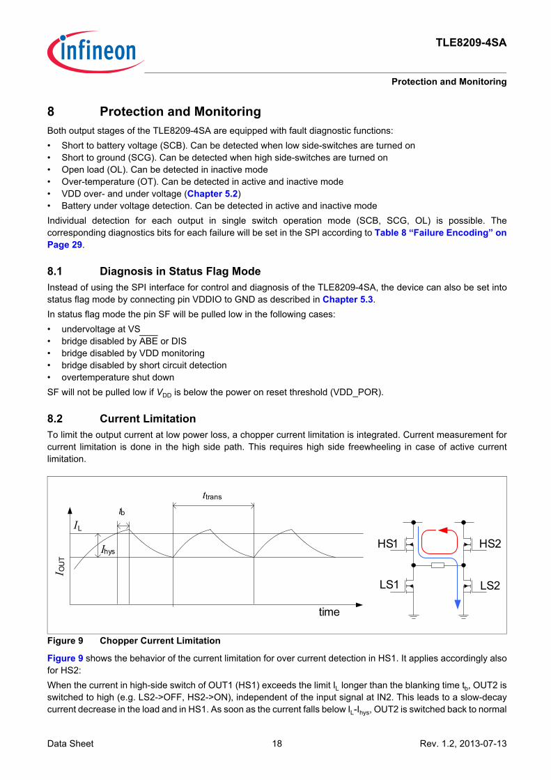
8.2 Current LimitationTo limit the output current at low power loss, a chopper current limitation is integrated. Current measurement forcurrent limitation is done in the high side path. This requires high side freewheeling in case of active currentlimitation.
Figure 9 Chopper Current Limitation
Figure 9 shows the behavior of the current limitation for over current detection in HS1. It applies accordingly alsofor HS2:When the current in high-side switch of OUT1 (HS1) exceeds the limit IL longer than the blanking time tb, OUT2 isswitched to high (e.g. LS2->OFF, HS2->ON), independent of the input signal at IN2. This leads to a slow-decaycurrent decrease in the load and in HS1. As soon as the current falls below IL-Ihys, OUT2 is switched back to normal
I OU
T
time
IL
ttrans
LS2
HS2
tb
IhysHS1
LS1

Data Sheet 19 Rev. 1.2, 2013-07-13
TLE8209-4SA
Protection and Monitoring
operation, i.e. the outputs follow the inputs according to the truth table. The current limit IL can be programmed tofour different values by setting the SPI bits CL1 and CL2 in the SPI configuration register. To avoid high chopperfrequencies the time between two transients ttrans is limited.
Current limitation is available in H-bridge operation mode, not in single switch operation mode. This means, thatthe current limit, current limit hysteresis and blanking time has no effect in single switch operation mode.
8.3 Temperature Dependent Current ReductionFor TILR < Tj < TSD the current limit decreases from IL as set by the SPI to IL_TSD = 2.5 A typ. as shown inFigure 10.
Figure 10 Temperature Dependent Current Reduction
8.4 Short Circuit to Ground
Figure 11 Short to Ground Detection
A
Tj [°C]TILR(typ. 165°C)
tolerance of temperature dependent current
reduction
range of over-temperature shut-down
TSD(min. 175°C)
IL
IL_TSD(typ. 2.5A)
IOUT
IL
time
tb
IOUK
IN1
tDF_H
t<tb
OUT1
curre
nt
short circuit detected
current tracking
output off
Ihys
current limitation active
tDF_OFF
Short
IN2tristate
OUT2 tristate

TLE8209-4SA
Protection and Monitoring
Data Sheet 20 Rev. 1.2, 2013-07-13
The short circuit to ground detection is activated when the current through one of the high side switches rises overthe threshold IOUK and remains higher than IOUK for at least the filter time tDF_H within the blanking time tb. The output stage in which the short circuit was detected will be switched off within tDF_OFF. In H-bridge mode also the other output will be switched off after a short delay of tDF_del . In single switch mode only the affected output will be switched off.
8.5 Short Circuit to Battery
A short circuit to battery is detected in the same way as a short circuit to ground, only in the low side switch instead of the high side switch.
8.6 Short Circuit across the LoadShort circuit over load is indicated by two failures - short circuit to ground on one output and short circuit to batteryon the other output. Both failure bits will be set in the SPI diagnostics register. Both output stages will be turned off.
8.7 OvertemperatureIn case of high DC-currents, insufficient cooling or high ambient temperature, the chip temperature may rise abovethe thermal shut-down temperature TSD (see Figure 10). In that case, all output transistors are turned off.
8.8 Undervoltage Shut-DownIf the supply voltage at the VS pins falls below the undervoltage detection threshold VUV_OFF, the outputs switchesare turned off. As soon as VS rises above VUV_ON again, the device is returning to normal operation.
8.9 Open Load DiagnosisOpen load diagnosis is only possible if outputs are switched off by DIS or ABE. The diagnostic current sources aredeactivated in status flag mode. Diagnostic current sources are disconnected if outputs are active. That meansthat the diagnostic current sources are also disconnected if the outputs are deactivated due to short circuit. Theopen load detection in H-bridge mode is different from the open load detection in single switch mode.
Open Load Detection in H-Bridge mode
Figure 12 Open Load Detection in H-Bridge Mode
VDD
+-
Vref_L
OUT1
OUT1_L +-
Vref_L
OUT2
OUT2_L

Data Sheet 21 Rev. 1.2, 2013-07-13
TLE8209-4SA
Protection and Monitoring
Open Load Detection in Single Switch Mode
Figure 13 Open Load Detection in Single Switch Mode
Table 3 Open Load Detection in H-Bridge ModeVOUT1 OUT1_L VOUT2 OUT2_L Diagnostic Comment< Vref_L H < Vref_L H Load o.k. pull down current is stronger< Vref_L H > Vref_L L Load o.k. transient area> Vref_L L < Vref_L H Open Load> Vref_L L > Vref_L L Load o.k. transient area
Table 4 Open Load Detection in Single Switch ModeVOUTx (OFF State) OUTx_H OUTx_L Diagnostic CommentVOUTx < Vref_L L H o.k. Load to groundVref_L <VOUTx < Vref_H L L Open Load Output openVOUTx > Vref_H H L o.k. Load to VS
VDD
Vref_H
Vref_M
Vref_L-+
VDDVref_M
+-Vref_H
+-
Vref_L
OUTx
OUTx_H
OUTx_L

TLE8209-4SA
Protection and Monitoring
Data Sheet 22 Rev. 1.2, 2013-07-13
8.10 Electrical Characteristics
Electrical Characteristics: Protection and MonitoringVS = 5 V to 28 V; VDD = 5.0 V, Tj = -40 ⋅C to 150 ⋅C, all voltages with respect to ground, positive current flowinginto pin (unless otherwise specified)Pos. Parameter Symbol Limit Values Unit Test Conditions
Min. Typ. Max.Chopper Current Limitation8.10.1 Current Limit |IL1| 1.0 1.8 2.7 A -40 °C < Tj < TILR
Dependent on SPI setting; Default = IL3
8.10.2 |IL2| 3.3 4.8 5.78.10.3 |IL3| 6.0 7.8 9.28.10.4 |IL4| 9.0 10.6 12.38.10.5 Current Limit Hysteresis Ihys 0.0 0.3 0.4 A -40 °C < Tj < TILR
8.10.6 Blanking time tb 8 11 15 μs –
8.10.7 Time between transients ttrans 90 – 130 μs – Temperature Dependent Current Limitation1)
8.10.8 Current Limit at TSD IL_TSD 1.4 2.5 3.6 A – 8.10.9 Start of current limit
reductionTILR 150 165 – °C –
8.10.10 Thermal shut-down TSD 175 – – °C – 8.10.11 Range of temperature
dependent current reduction
TSD - TILR 20 25 30 °C –
Short Circuit Detection to GND8.10.12 Short circuit detection
current (HS)|IOUKH1| 2.5 6.3 7.5 A -40 °C < Tj < TILR
Dependent on SPI-setting for |IL|; Default = IOUKH3
8.10.13 |IOUKH2| 5.5 9.0 11.08.10.14 |IOUKH3| 8.5 11.7 13.58.10.15 |IOUKH4| 10.5 14.2 17.48.10.16 Current tracking |IOUKH1| - |IL1| 1.5 4.4 5.5 A8.10.17 |IOUKH2| - |IL2| 2.0 4.2 5.58.10.18 |IOUKH3| - |IL3| 2.0 3.9 5.08.10.19 |IOUKH4| - |IL4| 1.5 3.7 5.0Short Circuit Detection to VS8.10.20 Short circuit detection
current (LS)|IOUKL1| 2.5 4.6 6.5 A -40 °C < Tj < TILR
Dependent on SPI-setting for |IL|; Default = IOUKL3
8.10.21 |IOUKL2| 5.0 8.1 10.08.10.22 |IOUKL3| 7.5 10.0 11.58.10.23 |IOUKL4| 10.5 14 17.48.10.24 Current tracking |IOUKL1| - |IL1| 1.0 2.8 5.0 A8.10.25 |IOUKL2| - |IL2| 1.0 3.3 5.58.10.26 |IOUKL3| - |IL3| 0.5 2.2 5.58.10.27 |IOUKL4| - |IL4| 0.3 3.4 7.0

Data Sheet 23 Rev. 1.2, 2013-07-13
TLE8209-4SA
Protection and Monitoring
Short Circuit Detection Timing8.10.28 Delay time for fault
detectiontDF_H, tDF_L 1 2 5 µs –
8.10.29 Time from detected fault to high impedance of output1)
tDF_OFF – – 4 µs –
8.10.30 Delay time between switching off of the output stages in short circuit
tDF_del 5 17 40 µs –
Open Load 8.10.31 Open Load Diagnostic
Filter Time1)tOL_DIAG 60 – 135 µs –
8.10.32 Low Diagnosis Threshold Vref_L 0.4 * VDD - 0.2
0.4 * VDD
0.4 * VDD + 0.2
V –
8.10.33 High Diagnosis Threshold Vref_H 0.8 * VDD - 0.2
0.8 * VDD
0.8 * VDD + 0.2
V –
8.10.34 Diagnosis Bias Voltage Vref_M 0.6 * VDD - 0.2
0.6 * VDD
0.6 * VDD + 0.2
V –
8.10.35 Positive Diagnostic Current (pull down current source)
IDIA_P 300 620 980 µA VOUTx = 14 V8.10.36 270 610 980 µA VOUTx = Vref_H
8.10.37 Negative Diagnostic Current
IDIA_N -350 -240 -100 µA VOUTx = 0 V8.10.38 -350 -210 -80 µA VOUTx = Vref_L
8.10.39 Ratio of current sources (Pos/Neg)
RatioI_DIA 2 2.9 4 – –
Undervoltage 8.10.40 Undervoltage at VS VUV OFF 3.1 3.7 4.4 V Switch off threshold
VUV ON 3.3 3.9 4.6 V Switch on thresholdVUV HY 100 200 400 mV Hysteresis
8.10.41 VS Undervoltage Detection Filter Time1)
tUV – – 1.5 µs
1) Not subject to production test; specified by design.
Electrical Characteristics: Protection and MonitoringVS = 5 V to 28 V; VDD = 5.0 V, Tj = -40 ⋅C to 150 ⋅C, all voltages with respect to ground, positive current flowinginto pin (unless otherwise specified)Pos. Parameter Symbol Limit Values Unit Test Conditions
Min. Typ. Max.

TLE8209-4SA
SPI Interface
Data Sheet 24 Rev. 1.2, 2013-07-13
9 SPI InterfaceThe serial SPI interface establishes a communication link between TLE8209-4SA and the systemsmicrocontroller. The TLE8209-4SA always operates in slave mode whereas the controller provides the masterfunction. The maximum baud rate is 2 MBaud.By applying an active slave select signal at SS the TLE8209-4SA is selected by the SPI-master. SI is the datainput (Slave In), SO the data output (Slave Out). Via SCK (Serial Clock Input) the SPI-clock is provided by themaster. In case of inactive slave select signal (High) the data output SO goes into tristate.The first two bits of an instruction may be used to establish an extended device-addressing. This gives theopportunity to operate up to 4 Slave-devices sharing one common SS signal from the Master-Unit (see Figure 16).
Figure 14 SPI Block Diagram
9.1 General SPI Characteristics
1. During active reset conditions the SPI is driven into its default state. The output SO is set to high impedance(tristate). When reset becomes inactive, the state machine enters into a wait state for the next instruction.
2. If the slave select signal at SS is inactive (high), the state machine is forced to wait for the following instruction. 3. During active (low) state of the select signal SS the falling edge of the serial clock signal SCK will be used to
latch the input data at SI. Output data at SO are driven with the rising edge of SCK. Further processing of thedata according to the instruction (i.e. modification of internal registers) will be triggered by the rising edge ofthe SS signal.
4. In order to establish the option of extended addressing the upper two bits of the instruction byte (i.e. the firsttwo SI bits of a frame) are reserved to send a chip address. To avoid a bus conflict the output SO will remaintristate during the addressing phase of a frame (i.e. until the address bits are recognized as a valid chip
SS
SCK
SI
SOshift-register
SPI-Control:
-> state machine-> clock counter-> instruction recognition
DIA_REGDiagnostics
8
8
ORABE
DISReset

Data Sheet 25 Rev. 1.2, 2013-07-13
TLE8209-4SA
SPI Interface
address). If the chip address does not match, the according frame will be ignored and SO remains tristate forthe complete frame.
5. Verification byte: Simultaneously to the receipt of an SPI instruction the TLE8209-4SA transmits a verificationbyte via the output SO to the controller. This byte indicates regular or irregular operation of the SPI. It containsan initial bit pattern and a flag indicating an invalid instruction of the previous access.
6. On a read access the data bits at the SPI input SI are rejected. During a valid write access the SPI will transmitthe data byte "00hex" at the output SO after having sent the verification byte.
7. An instruction is invalid if one of the following conditions is fulfilled:- an unused instruction code is detected (see tables with SPI instructions).- the previous transmission is not completed in terms of internal data processing.- the number of SPI clock pulses (falling edge) counted during active SS differs from exactly 16 clock pulses.If an unused instruction code occurres, the data byte “FFhex” (no error) will be transmitted after having sent the verification byte. This transmission takes place within the same SPI-frame that contained the unused instruction byte. If an invalid instruction is detected, bit TRANS_F in the following verification byte (next SPI-transmission) is set to HIGH. The TRANS_F bit must not be cleared before it has been sent to the microcontroller.
9.2 SPI CommunicationThe 16 input bits consist of the SPI instruction byte and an input data byte. The 16 output bits consist of theverification byte and the output data byte (see also Figure 15). The definition of these bytes is given in thesubsequent sections. The access mode of the registers is described in the column “Type” (r = read, w = write).
Figure 15 SPI Communication
9.2.1 Instruction ByteThe upper 2 bit of the instruction byte contain the chip address. The chip address of the TLE8209-4SA is ’00’.During read access, the output data according to the register requested in the instruction byte are applied to SOwithin the same SPI frame. That means, the output data corresponding to an instruction byte sent during one SPIframe are transmitted to SO during the same SPI-frame
07 6 5 4 3 2 1 0 7 6 5 4 3 2 1
SI
SCK
SS
SO
SPI Instruction input data-byteMSB LSB
Verification byte output data-byteMSB LSB MSB LSB

TLE8209-4SA
SPI Interface
Data Sheet 26 Rev. 1.2, 2013-07-13
Figure 16 Bus Arbitration by Chip Address
Table 5 SPI Instruction Format
7 6 5 4 3 2 1 0
CPAD1 CPAD0 INSTR5 INSTR4 INSTR3 INSTR2 INSTR1 INSTR0
Field Bits Type DescriptionCPAD1:0 7:6 w Chip Address (00B)INSTR5:0 5:0 w SPI Instruction (encoding)
Z
07 6 5 4 3 2 1 0 7 6 5 4 3 2 1
7 12345670123456 0SI
SCK
SS
1234567012345SO 0
Address sent bymaster is "00B"
SO remains tristatedafter SS active
Correct addres is recognized,data transmitted to SO
Z
07 6 5 4 3 2 1 0 7 6 5 4 3 2 1
7 12345670123456 0SI
SCK
SS
SO
Address sent by masteris different from "00 B"
SO remains tristatedafter SS active
Correct addres is not recognized, SOremains tristated and SI data are ignored

Data Sheet 27 Rev. 1.2, 2013-07-13
TLE8209-4SA
SPI Interface
9.2.2 Verification Byte
9.2.3 Device Identifier and RevisionThe IC’s identifier (device ID) and revision number are used for production test purposes and features plug & playfunctionality depending on the systems software release. The two numbers are read-only accessible via the SPI-instructions RD_ID and RD_REV as described in Section 9.2.1. The device ID is defined to allow identification ofdifferent IC-types by software and is fixed for the TLE8209-4SA.The revision number may be utilized to distinguish different states of hardware and is updated with each redesignof the TLE8209-4SA. It is divided into an upper 4 bit field reserved to define revisions (SWR) corresponding tospecific software releases and a lower 4 bit field utilized to identify the actual mask set revision (MSR).
Table 6 SPI Instruction SetCommand SPI Instruction Byte DescriptionRD_ID 0000 0000 Read identifierRD_REV 0000 0011 Read versionRD_DIA 0000 1001 Read diagnostics registerRD_CONFIG 0011 0000 Read power stage configurationRD_STATCON 0011 1100 Read VDD monitoring statusWR_CONFIG 0010 1000 Write power stage configurationWR_STATCON 0001 1000 Write VDD monitoring statusall other instructions 00xx xxxx Unused - TRANS_F is set to high, ff_hex is sent as data bit.all other chip addr. xxxx xxxx Invalid address - SO remains tristate during entire SPI-frame.
Table 7 Verification Byte Format
7 6 5 4 3 2 1 0
VER6 VER5 VER4 VER3 VER2 VER1 VER0 TRANS_F
Field Bits Type DescriptionVER6 7 r Fixed to tristate (Z)VER5 6 r Fixed to tristate (Z)VER4 5 r Fixed to high (1)VER3 4 r Fixed to low (0)VER2 3 r Fixed to high (1)VER1 2 r Fixed to low (0)VER0 1 r Fixed to high (1)TRANS_F 0 r Transfer failure:
1B Error detected during previous transfer0B Previous transfer was recognized as valid
TLE8209-4SA
SPI Interface
Data Sheet 28 Rev. 1.2, 2013-07-13
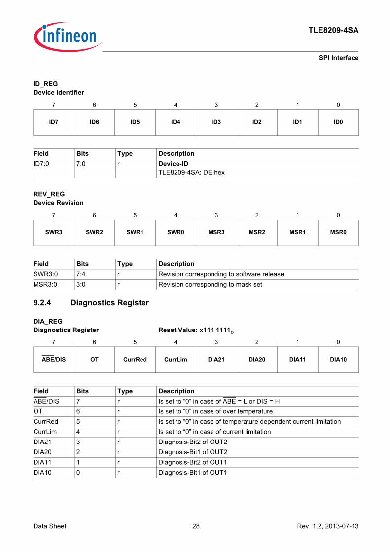
9.2.4 Diagnostics Register
ID_REGDevice Identifier
7 6 5 4 3 2 1 0
ID7 ID6 ID5 ID4 ID3 ID2 ID1 ID0
Field Bits Type DescriptionID7:0 7:0 r Device-ID
TLE8209-4SA: DE hex
REV_REGDevice Revision
7 6 5 4 3 2 1 0
SWR3 SWR2 SWR1 SWR0 MSR3 MSR2 MSR1 MSR0
Field Bits Type DescriptionSWR3:0 7:4 r Revision corresponding to software releaseMSR3:0 3:0 r Revision corresponding to mask set
DIA_REGDiagnostics Register Reset Value: x111 1111B
7 6 5 4 3 2 1 0
ABE/DIS OT CurrRed CurrLim DIA21 DIA20 DIA11 DIA10
Field Bits Type DescriptionABE/DIS 7 r Is set to “0” in case of ABE = L or DIS = HOT 6 r Is set to “0” in case of over temperatureCurrRed 5 r Is set to “0” in case of temperature dependent current limitationCurrLim 4 r Is set to “0” in case of current limitationDIA21 3 r Diagnosis-Bit2 of OUT2DIA20 2 r Diagnosis-Bit1 of OUT2DIA11 1 r Diagnosis-Bit2 of OUT1DIA10 0 r Diagnosis-Bit1 of OUT1

Data Sheet 29 Rev. 1.2, 2013-07-13
TLE8209-4SA
SPI Interface
Note:The bit ABE/DIS shows directly the status of inputs ABE and DIS. It is set to ‘0’ if the power stages are disabledby ABE or DIS.The bits OT, CurrRed and CurrLim are latched. They will be reset with each read access. If the failure condition isstill present the according bits are set again. Undervoltage at VS is reported and the outputs are switched off as long as the undervoltage condition is present.The previous setting of the DIAx bits is masked but not reset. Once the supply voltage is back in the operatingrange the diagnostic bits DIAxx will return to their setting before VS undervoltage. The outputs will return to normaloperation.Detection of short circuit will switch of the output stages. In single half bridge operation only the affected output isswitched off. In H-Bridge mode both outputs are shut down. The outputs remain off until the failure condition isremoved and the diagnosis register is reset.A short across the load may also be reported as SCG at one output and SCB at the other.
The diagnostic information DIAxx in the SPI interface is reset in the following cases:• Read out of DIA_REG: only bit 4, 5 and 6 will be reset• Enabling or disabling of the bridge via ABE or DIS• Undervoltage at VDD• Reset command via SPI
Table 8 Failure EncodingABE/DIS DIA21 DIA20 DIA11 DIA10 Description Comment
X 1 1 1 1 no failure1 X X 0 1 short circuit to battery at OUT1 (SCB1) latched1 X X 1 0 short circuit to ground at OUT1 (SCG1) latched1 X X 1 1 no error detected at OUT11 0 1 X X short circuit to battery at OUT2 (SCB2) latched1 1 0 X X short circuit to ground at OUT2 (SCG2) latched1 1 1 X X no error detected at OUT21 0 1 1 0 short circuit accross load (HS1+LS2 active) latched1 1 0 0 1 short circuit accross load (HS2+LS1 active) latchedX 0 0 0 0 Undervoltage at pin VS not latched0 1 1 0 0 open load (H-Bridge) latched0 1 1 X 0 open load at OUT1 (single switch operation) latched0 1 1 0 X open load at OUT2 (single switch operation) latched

TLE8209-4SA
SPI Interface
Data Sheet 30 Rev. 1.2, 2013-07-13
9.2.5 Configuration Register
9.2.6 STATCON Register
CONFIG_REGConfiguration Register Reset Value: 1111 1010B
7 6 5 4 3 2 1 0
MODE MUX SIN1 SIN2 CL1 CL2 RESET SL
Field Bits Type DescriptionMODE 7 wr ’1’: H-bridge mode
’0’: single output stages (for current levels 1 to 3 only)MUX 6 wr ’1’: control by parallel inputs IN1 and IN2
’0’: control by SPI bits SIN1 and SIN2SIN1 5 wr control of OUT1 if MUX=’0’SIN2 4 wr control of OUT2 if MUX=’0’CL1 3 wr current limitation level (see table below)CL2 2 wr current limitation level (see table below)RESET 1 wr ’0’: reset of digital logicSL 0 wr slew rate setting
’1’: slow ’0’: fast
Table 9 Current Limitation LevelsCL1 CL2 Current Level Typical Current
0 0 1 1.8 A0 1 2 4.8 A1 0 3 (default) 7.8 A1 1 4 10.6 A
STATCON_REGSTATCON Register Reset Value: 1101 1xxxB
7 6 5 4 3 2 1 0
CONFIG2 CONFIG1 CONFIG0 DIACLR2 DIACLR1 STATUS2 STATUS1 STATUS0
Field Bits Type DescriptionCONFIG2 7 wr VDD threshold test mode
’1’: VDD monitoring in normal operation’0’: VDD thresholds are changed according to CONFIG1

Data Sheet 31 Rev. 1.2, 2013-07-13
TLE8209-4SA
SPI Interface
CONFIG1 6 wr changes thresholds in VDD threshold test mode (CONFIG2=’0’)’1’: increase lower threshold of VDD monitoring to test switch off path’0’: decrease upper threshold of VDD monitoring to test switch off path
CONFIG0 5 wr latch function for overvoltage at VDD’1’: overvoltage at VDD latched’0’: overvoltage at VDD not latched
DIACLR2 4 wr ’0’: clears diagnosis of OUT2always returns ’1’ at read access
DIACLR1 3 wr ’0’: clears diagnosis of OUT1always returns ’1’ at read access
STATUS2 2 r returns level at ABESTATUS1 1 r ’0’: under voltage at VDD
’1’: VDD voltage above lower limitSTATUS0 0 r 0’: over voltage at VDD
’1’: VDD voltage below upper limit
Field Bits Type Description

TLE8209-4SA
SPI Interface
Data Sheet 32 Rev. 1.2, 2013-07-13
9.2.7 Contents of the SPI registers after a reset condition
Note: The registers for device identifier and revision (ID_REG and REV_REG) are not affected by reset.
POR: Reset due to VDD power upSPIR: Reset via SPI by writing 0 into the RESET of CONFIG_REGABE/DISR: Reset due to enabling or disabling the power stages via DIS or ABE (edge triggered)DISR: Reset due to a disabled power stage by DIS or ABE (level triggered)RDR: Reset due to a read access to DIA_REGDIACLR1: Reset via SPI by writing 0 into the DIACLR1 of STATCON_REGDIACLR2: Reset via SPI by writing 0 into the DIACLR2 of STATCON_REGSFMODE: Reset by setting the TLE8209-4SA into the Status Flag Mode (VDDIO = 0V)
x: No change
Note: If a reset condition is not listed for a particular register it has no effect on the contents of this register.
DIA_REG7 6 5 4 3 2 1 0
ABE/DIS OT CurrRed CurLim DIA21 DIA20 DIA11 DIA10POR x 1 1 1 1 1 1 1SPIR x 1 1 1 1 1 1 1ABE/DISR x 1 1 1 1 1 1 1RDR x 1 1 1 x x x xDIACLR1 x x x x x x 1 1DIACLR2 x x x x 1 1 x x
CONFIG_REG7 6 5 4 3 2 1 0
MODE MUX SIN1 SIN2 CL1 CL2 RESET SLPOR 1 1 1 1 1 0 1 0SPIR 1 1 1 1 1 0 1 0DISR x 1 1 1 x x 1 xSFMODE 1 1 1 1 1 0 1 0
STATCON_REG7 6 5 4 3 2 1 0
CONFIG2 CONFIG1 CONFIG0 DIACLR2 DIACLR1 STATUS2 STATUS1 STATUS0POR 1 1 0 1 1 x x xSPIR 1 1 0 1 1 x x xSFMODE 1 1 0 1 1 x x x

Data Sheet 33 Rev. 1.2, 2013-07-13
TLE8209-4SA
SPI Interface
9.3 Electrical Characteristics SPI
Figure 17 SPI Timing
Electrical Characteristics: SPI InterfaceVS = 5 V to 28 V; VDD = 5.0 V; VDDIO = 2.9 V to 5.5 V, Tj = -40 ⋅C to 150 ⋅C, all voltages with respect to ground,positive current flowing into pin (unless otherwise specified)Pos. Parameter Symbol Limit Values Unit Test Conditions
Min. Typ. Max.SPI-Timing (see Figure 17)1)
1) All timing parameters specified by design - not subject to production test
9.3.1 Cycle-time (1) tcyc 490 – – ns referred to master9.3.2 Enable Lead Time (2) tlead 50 – – ns referred to master9.3.3 Enable Lag Time (3) tlag 150 – – ns referred to master9.3.4 Data Valid (4)
H->L: VSCK=2V -> VSO=0.2 VDDIOL->H: VSCK=2V -> VSO=0.8 VDDIOif VDDIO < 4.5V:L->H: VSCK=2V -> VSO=0.7 VDDIO
tv ––
––
150230
ns CL = 200 pFCL = 350 pFreferred to TLE8209-4
9.3.5 Data Setup Time (5) tsu 40 – – ns referred to master9.3.6 Data Hold Time (6) th 40 – – ns referred to master9.3.7 Disable Time (7) tdis – – 100 ns referred to TLE8209-49.3.8 Transfer Delay (8) tdt 250 – – ns referred to master9.3.9 Disable Lead Time (9) tdld 250 – – ns referred to master9.3.10 Disable Lag Time (10) tdlg 250 – – ns referred to master9.3.11 Access time (11) tacc 8.35 – – μs referred to master
SS
SO
SI
SCK
1 2 3
4
5 6
7
8 9
10
11
tristate Bit (n-3) Bit (n-4)…1 Bit 0; LSB
MSB IN Bit (n-2) Bit (n-3) Bit (n-4)…1 LSB IN
n=16
TLE8209-4SA
Application Information
Data Sheet 34 Rev. 1.2, 2013-07-13
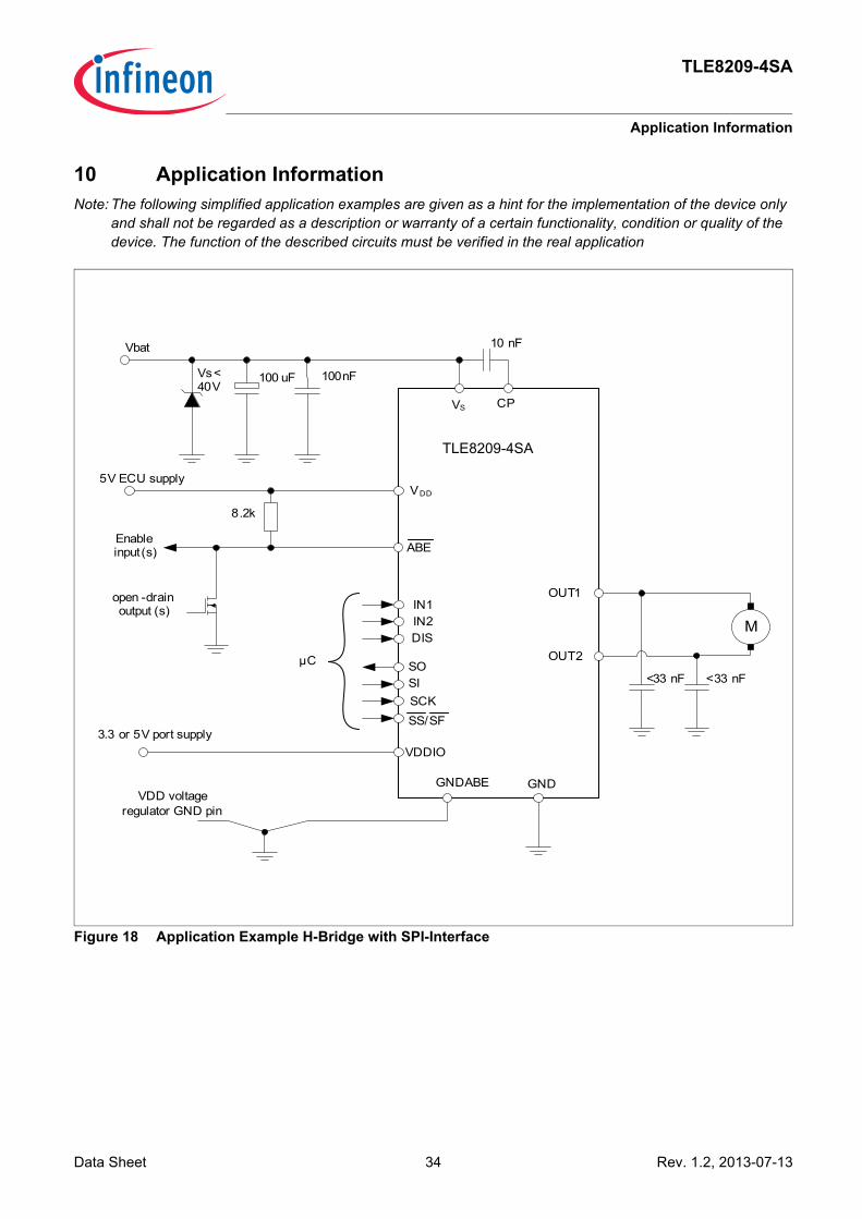
10 Application InformationNote: The following simplified application examples are given as a hint for the implementation of the device only
and shall not be regarded as a description or warranty of a certain functionality, condition or quality of the device. The function of the described circuits must be verified in the real application
Figure 18 Application Example H-Bridge with SPI-Interface
VDD
ABE
GNDABE
SOSI
DIS
SCKSS/SF
VDDIO
IN1IN2
OUT1
GND
VS
OUT2
M
CP
10 nFVbat
5V ECU supply
Enable input(s)
open -drain output (s)
3.3 or 5V port supply
<33 nF<33 nFµC
100nF100 uFVs<40V
8.2k
VDD voltage regulator GND pin
TLE8209-4SA

Data Sheet 35 Rev. 1.2, 2013-07-13
TLE8209-4SA
Application Information
Figure 19 Application Example with Status Flag
Figure 20 Application Examples for Overvoltage and Reverse-Voltage Protection
VDD
ABE
GNDABE
DIS
VDDIO
IN1IN2
OUT1
GND
VS
OUT2
M
CP
10 nFVbat
5V ECU supply
Enable input (s)
open -drain output (s)
<33 nF<33 nF
uC
100 nF100 uFVs<40V
47k
SOSISCK
SS/SF
8.2k3.3 or 5V port supply
VDD voltage regulator GND pin
TLE8209-4SA
100 nF100µFmain relay
ignition switch
VS
battery
Vs <
40V
Reverse polarity protection via main relay

TLE8209-4SA
Package Outlines TLE8209-4SA
Data Sheet 36 Rev. 1.2, 2013-07-13
11 Package Outlines TLE8209-4SA
Figure 21 PG-DSO-20-65 (Plastic Dual Small Outline Package)
Green Product (RoHS compliant)To meet the world-wide customer requirements for environmentally friendly products and to be compliant withgovernment regulations the device is available as a green product. Green products are RoHS-Compliant (i.ePb-free finish on leads and suitable for Pb-free soldering according to IPC/JEDEC J-STD-020).
Heatslug1101 10
Index Marking
Does not include plastic or metal protrusion of 0.15 max. per side
1 x 45˚
(Mold)15.9 1)±0.15
A
-0.2
(Metal)
13.7
0+0
.1+0.130.4
20 11
0.25 M A
1.27
1.1±0.1
(Heatslug)15.74 ±0.1
(Met
al)
0.25
Heatslug(Mold)
20x
11
3.2
14.2 ±0.3
20 ±0.1
0.95
3.25
3.5
MA
X.
0.1
1.3
±0.1
-0.0
2+0
.07
6.3
0.25
±0.15
2.8
11 1)
B
(Met
al)
5.9
B
±0.1
±0.15
5˚±3
˚
1)
Bottom View
1.27
1.83
9 x 1.27 = 11.43
13.4
8
0.68
GPS05791
Footprint:
hlg09550
You can find all of our packages, sorts of packing and others in ourInfineon Internet Page: http://www.infineon.com/packages Dimensions in mm
Data Sheet 37 Rev. 1.2, 2013-07-13
TLE8209-4SA
Revision History
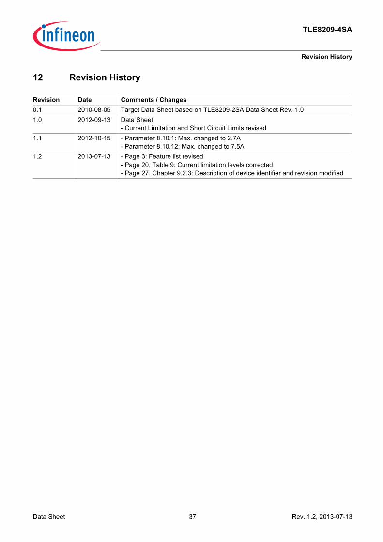
12 Revision History
Revision Date Comments / Changes0.1 2010-08-05 Target Data Sheet based on TLE8209-2SA Data Sheet Rev. 1.01.0 2012-09-13 Data Sheet
- Current Limitation and Short Circuit Limits revised1.1 2012-10-15 - Parameter 8.10.1: Max. changed to 2.7A
- Parameter 8.10.12: Max. changed to 7.5A1.2 2013-07-13 - Page 3: Feature list revised
- Page 20, Table 9: Current limitation levels corrected- Page 27, Chapter 9.2.3: Description of device identifier and revision modified

Edition 2013-07-13Published byInfineon Technologies AG81726 Munich, Germany© 2013 Infineon Technologies AGAll Rights Reserved.
Legal DisclaimerThe information given in this document shall in no event be regarded as a guarantee of conditions or characteristics. With respect to any examples or hints given herein, any typical values stated herein and/or any information regarding the application of the device, Infineon Technologies hereby disclaims any and all warranties and liabilities of any kind, including without limitation, warranties of non-infringement of intellectual property rights of any third party.
InformationFor further information on technology, delivery terms and conditions and prices, please contact the nearest Infineon Technologies Office (www.infineon.com).
WarningsDue to technical requirements, components may contain dangerous substances. For information on the types in question, please contact the nearest Infineon Technologies Office.Infineon Technologies components may be used in life-support devices or systems only with the express written approval of Infineon Technologies, if a failure of such components can reasonably be expected to cause the failure of that life-support device or system or to affect the safety or effectiveness of that device or system. Life support devices or systems are intended to be implanted in the human body or to support and/or maintain and sustain and/or protect human life. If they fail, it is reasonable to assume that the health of the user or other persons may be endangered.