lab 2: amplifier project - carleton universitysdemtche/elec3509/documents/lab2_2011.pdfelec 3509...
TRANSCRIPT

ELEC 3509 Electronics II Lab 2
Lab 2: Amplifier Project Schedule for This Lab: Day 1: Single‐transistor and 2‐transistor amplifiers Day 2: Cascode Amplifier Design and Development Day 3: Continuation of week 2. Your amplifier should be working by the start of this period Milestones: Day 1: Transistor amplifier results witnessed Day 2: Design calculations presented orally to teaching assistants and witnessed Day 3: Demonstration of working amplifier showing satisfactory performance and understanding
The report should discuss all of the material you do including the material in Day 1. You must discuss your design and show the complete process, from calculating your required specifications to a detailed plot of measurements.
Purpose:
The purpose of this laboratory is to investigate the use of BJTs as amplifier circuit elements. First, the three basic configurations (CE, CC and CB) are observed. Then, by proper combinations and permutations, 2‐transistor amplifier configurations can be studied for improved gain‐bandwidth performance. Finally, a specific configuration is required to be designed to meet or exceed a prescribed set of specifications.
Although in all likelihood you will probably never need to design discrete transistor amplifiers, the steps that you will follow to design, build and test your circuit are common to many engineering problems in real life.
Introduction:
Before starting this project, read Sedra and Smith, "Micro‐Electronic Circuits", SS4 pp. 276‐295, 602‐635 and 641‐644 (SS5 pp. 436‐442, 460‐485, 491‐503, 588‐648). Also, read the relevant class notes, and the sections of this laboratory outline dealing with design approaches.
Day 1: Single Transistor amplifiers and Two‐Transistor Amplifiers In this part, you will be constructing and making measurements of 3 types of single amplifier
configurations and by doing so, identify the strengths and weaknesses of each one. Afterwards you will be combining them in pairs and again make measurements of 3 pairs and again identify the strengths and weaknesses of each one. This will give you some experience when you design your own amplifier the next day, and will give you some background to discuss the design.
Part 1: Circuit Construction and D.C. Measurements For this day, you will need to construct the circuit shown in Figure 2.1. This circuit contains 3 amplifiers
(you need to build all 3 at the same time on the same board). As you will be making high frequency measurements, you should keep your circuits neat and clean with as short wires as possible. Note that building this circuit in advance on your given breadboard will save you a lot of time.

ELEC 3509 Electronics II Lab 2
Figure 2.1 Schematic showing the 3 single transistor amplifiers
The component values are as follows (i.e. R1.1=R1.2=R1.3=100kOhm):
Component (CC) Component (CE) Component (CB) Component value
R1.1 R1.2 R1.3 100 kOhm
R2.1 R2.2 R2.3 39 kOhm
RC1 RC2 RC3 5.6 kOhm
RE1 RE2 RE3 3.3 hOhm
CE2 100 uF
CB3 1uF
Note: RC1 is to be present when verifying the DC operating point. However, when performing your AC measurements, it is to be shorted out. Prelab:
Why does RC1 need to be made 0 when testing the amplifier? Why do you need to have it when checking the DC operating point? Could we instead use a capacitor like we do for the CE and CB amplifiers? Why do we need CE2 and CB3? Why can’t we just short those nodes to ground as we did for the CC amplifier? Experiment:
Build the D.C. bias network on your circuit board. Your layout of the circuit should be neat and compact such that access to the three terminals (E, B and C) of each and every transistor can be made easily. Measure all resistors before connecting the circuit to the bench supply.
For each and every transistor, take D.C. measurements of all relevant voltages (VB, VE, VC and VCC). Determine the terminal currents from the following relationships:
ELEC 3509 Electronics II Lab 2
Note that IB is calculating by subtracting two large values that are very similar, and so the error will be
large if you are not accurate. Check if IE ≈ I B + IC and determine the DC value of β by calculating
Define the "AC ground" node of the three transistors as follows: o The first transistor is to be connected as a common‐collector amplifier. Thus, the collector should
be by‐passed to ground either by a capacitor, or, by replacing RC1 with a short‐circuit to VCC which is equivalent to an AC ground.
o The second transistor is to be connected as a common‐emitter amplifier by connecting a large value (say 100µF) capacitor CE2 from E2 to ground.
o The third transistor is to be connected as a common‐base amplifier by connecting a capacitor CB3 (CB3 ≥ 1 µF) from B3 to ground.
Report: Briefly summarize the results you have obtained here. As this is just preparatory work for the next section, there probably won’t be much you can discuss.
Part 2: AC Measurements for Single‐Transistor Amplifiers
Pre‐lab: Using the formulas in the notes/textbook, identify the expected gain, input and output impedance, and
high/low frequency cut‐off points of each amplifier. For component parameters, use the values you measured in lab 1, or make reasonable assumptions.
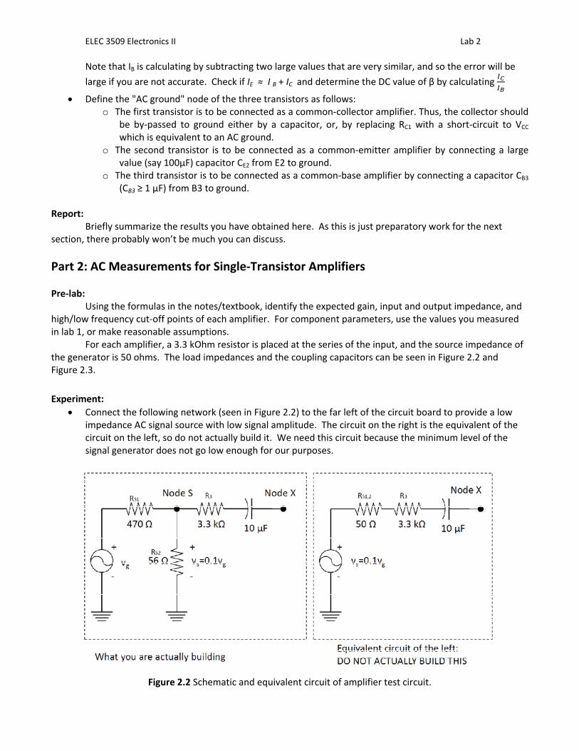
For each amplifier, a 3.3 kOhm resistor is placed at the series of the input, and the source impedance of the generator is 50 ohms. The load impedances and the coupling capacitors can be seen in Figure 2.2 and Figure 2.3.
Experiment:
Connect the following network (seen in Figure 2.2) to the far left of the circuit board to provide a low impedance AC signal source with low signal amplitude. The circuit on the right is the equivalent of the circuit on the left, so do not actually build it. We need this circuit because the minimum level of the signal generator does not go low enough for our purposes.
Figure 2.2 Schematic and equivalent circuit of amplifier test circuit.
ELEC 3509 Electronics II Lab 2
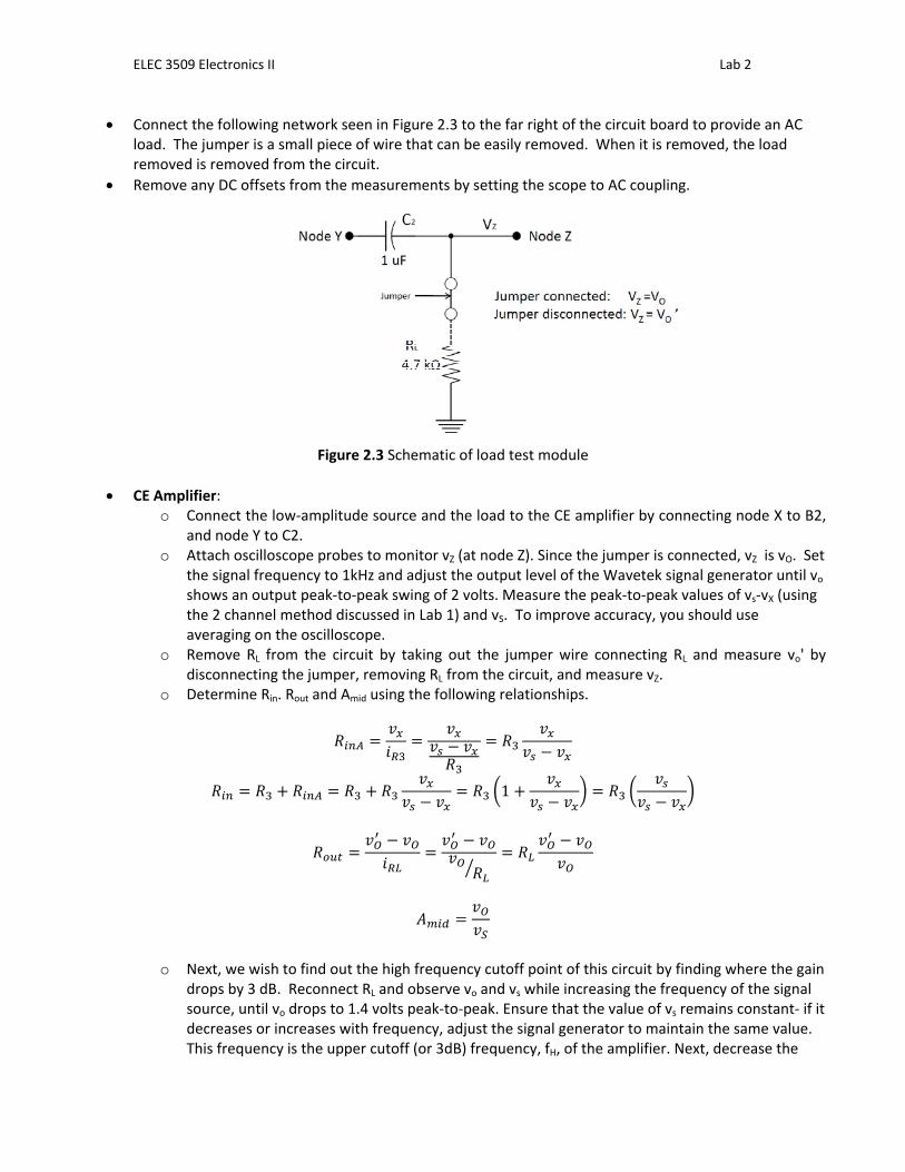
Connect the following network seen in Figure 2.3 to the far right of the circuit board to provide an AC load. The jumper is a small piece of wire that can be easily removed. When it is removed, the load removed is removed from the circuit.
Remove any DC offsets from the measurements by setting the scope to AC coupling.
Figure 2.3 Schematic of load test module
CE Amplifier: o Connect the low‐amplitude source and the load to the CE amplifier by connecting node X to B2,
and node Y to C2. o Attach oscilloscope probes to monitor vZ (at node Z). Since the jumper is connected, vZ is vO. Set
the signal frequency to 1kHz and adjust the output level of the Wavetek signal generator until vo shows an output peak‐to‐peak swing of 2 volts. Measure the peak‐to‐peak values of vs‐vX (using the 2 channel method discussed in Lab 1) and vS. To improve accuracy, you should use averaging on the oscilloscope.
o Remove RL from the circuit by taking out the jumper wire connecting RL and measure vo' by disconnecting the jumper, removing RL from the circuit, and measure vZ.
o Determine Rin. Rout and Amid using the following relationships.
1
o Next, we wish to find out the high frequency cutoff point of this circuit by finding where the gain
drops by 3 dB. Reconnect RL and observe vo and vs while increasing the frequency of the signal source, until vo drops to 1.4 volts peak‐to‐peak. Ensure that the value of vs remains constant‐ if it decreases or increases with frequency, adjust the signal generator to maintain the same value. This frequency is the upper cutoff (or 3dB) frequency, fH, of the amplifier. Next, decrease the

ELEC 3509 Electronics II Lab 2
frequency of the signal source until, again, vo drops to 1.4 volts peak‐to‐peak (again keeping vs constant) to obtain the lower cutoff frequency, fL, of the amplifier.
CC Amplifier o Connect node X to B1, and, node Y to E1. Also, connect the Wavetek output directly to node S
instead of through the 470 Ohm resistor. Again, you are aiming for a 2 V p‐p signal at the output. You may have to use the HI output of the Wavetek generator.
o Repeat the previous steps to get Rin, Rout, Amid, fH and fL of the CC amplifier.
CB Amplifier o Connect node X to E3, and, node Y to C3. Keep the Wavetek output connection to node S. Again,
you are aiming for a 2 V p‐p signal at the output. You may have to use the HI output of the Wavetek generator.
o Repeat the previous steps to get Rin, Rout, Amid, fH and fL of the CB amplifier.
Report:
For your report, show a complete table showing the values of calculated and measured of Rin, Rout, Amid, fH and fL for all 3 amplifiers. Comment on any differences you see between measured and calculated values. Explain any differences you see‐ don’t just ascribe it to a nebulous term such as “measurement error”‐ try to be as specific as possible. As a hint, recall that some of the AC measurements you made were probably not very accurate‐ identify those as a starting point.
Comment on the differences between all 3 amplifiers. Mathematically explain any differences you see: for instance if one amplifier has a higher gain, explain why that is so. Which ones are better for which tasks and why?

ELEC 3509 Electronics II Lab 2
Part 3: 2‐transistor Amplifiers In addition to the input signal coupling network and the output loading network, you will need an AC
coupling capacitor to connect from the first transistor to the second one. Since the large value capacitor is usually of the polarized type (electrolytic), make sure that you observe the polarity of the capacitor when connecting it to the circuit. Pre‐lab:
For each of the 3 2‐transistor amplifiers you will test in the section below, calculate Rin, Amid, fH and fL Experiment:
CE‐CB Amplifier Connect vi (node X) to B2, C2 to the plus side of the coupling capacitor (≥22µF), minus side of the coupling capacitor to E3, and, C3 to node Y. Now repeat all AC measurements to get the amplifier's parameters to get to get Rin, Amid, fH and fL (skip Rout).
CC‐CB Amplifier Connect vi (node X) to B1, E1 through a coupling capacitor (≥22µF) to E3, and keep the C3 to node Y connection. Repeat all measurements to get to get Rin, Amid, fH and fL (skip Rout).
CC‐CE Amplifier Keep vi connected to B1. Connect E1 to the minus side of the coupling capacitor, the plus side of the coupling capacitor to B2, and, C2 to node Y. Repeat all measurements to get to get Rin, Amid, fH and fL (skip Rout).
Report: For your report, show a complete table showing the values of measured of Rin, Amid, fH and fL for all 3 2‐
transistor amplifiers. On the same table, show the calculated values of these. Like with the 1 transistor amplifiers, explain any differences between the two set of values.
Comment on the differences between all 3 2‐transistor amplifiers. Like you did for the previous section, explain any differences in performance. Which ones are better for which tasks and why?
In weeks 2‐3 you will be designing a cascade amplifier, a variation on the CE‐CB amplifier. Identify what advantages this has over any of the single transistor amplifiers you tested. What are the advantages and disadvantages of using the cascade topology over any of the 2‐transistor topologies you just tested?

ELEC 3509 Electronics II Lab 2
Design Project for Days 2 and 3 During the remaining two weeks of the lab period you are expected to design the Cascode amplifier
similar to the bottom circuit on page 43, or right circuit on page 44 of your course notes (section 5). Of course you need to add RS and RL to the input and output of the circuit.
WEEK 2: Cascode Amplifier Design Review During this lab period students will present completed design calculations to a teaching assistant in the
lab, as well as to do preliminary tests on the amplifier itself. The purpose of this lab period is to try to catch design errors early, however, the onus for correctness must rest with the students themselves.
WEEK 3: Cascode Amplifier Demonstration
During this lab period students will present their final working amplifiers and demonstrate that they meet all of the stated requirements. Students are reminded to have their circuits working before they come to the lab in order that the teaching assistants may check out all students before the end of the period. Cascode Amplifier Requirements: You will need to design a cascode amplifier, which should be built and tested to meet the following requirements: 1. Magnitude of the voltage gain = SQRT(xxxxxx/50):± 10%, where xxxxxx represents your student number
modulo 500000. 2. RL = xxxxxx/25 ohms, rounded up to the nearest standard value stocked in the lab, i.e., decade multiples
of 1.0, 1.2, 1.5, 1.8, 2.2, 2.7, 3.3, 3.9, 4.7, 5.6, 6.8, and 8.2 k ohm. RL is to be the value of the load resistance driven by the circuit.
3. The high frequency cutoff fH is to be maximized. It must exceed 1 MHz. 4. The output voltage should be able to get to 2 V peak‐peak without appreciable distortion. We won’t
bother with numerical expressions so when designing this, use the guidelines outlined in the notes. Distortion is to be minimized by keeping the ac base voltage low. Again, use the guidelines in the notes.
5. No DC current may flow in RL and not DC current may flow into or out of the signal generator. 6. The low frequency fL must be less than 200 Hz and greater than 60 Hz. 7. The input and output impedances are left to the discretion of the designer, but their magnitudes at 1
kHz are to be determined by calculation and then measured. 8. Total circuit power is not to exceed 50 mW. 9. The transistors are all to be 2N3904 and/or 2N3906. 10. Collector currents in the transistors are to be 1.0 mA ±20%. 11. Power‐supply voltages are to be limited to +5 volts and/or +15 volts and/or ‐15 volts. 12. No adjustable components, e.g. trim‐pots, will be allowed. 13. The choice of all other components is left up to the designer. Design Approach‐ to be done by days 2‐3:
There is no unique solution to the amplifier design problem that has been laid out. The reason for this lack of uniqueness is the fact that there are more variables in the circuit than there are design parameters that have to be met. Consequently, a design solution requires the judicious fixing of some of the unspecified degrees of freedom in the circuit in order to begin to solve the problem. In almost all cases the solution requires iteration because the choices made to optimize one design parameter will often impact negatively on the other parameters.
In the next section an example design approach is presented for a single‐stage common‐emitter amplifier, along with many of the assumptions and approximations that are usually made in making the problem
ELEC 3509 Electronics II Lab 2
tractable. Much of what will be presented will provide insight into the design of the project amplifier, and indeed, much of it can be directly applied, or modified to suit. Example Design Approach for a Classical Common‐Emitter Amplifier:
As an example design approach we will consider the classical common‐emitter voltage amplifier with a four‐resistor bias network, as shown in Figure 2.4.
In designing such a circuit, it is generally first necessary to establish the DC bias conditions in the circuit. This action fixes many of the free variables thus making the subsequent design choices simpler. Unfortunately, at this point, the establishment of the DC bias conditions must be done with only a qualitative understanding of their implications on the other design parameters, likely making the solution sub‐optimal. However, it does provide the most efficient starting point for the design.
Following the establishment of the DC bias conditions, the AC characteristics can be set. If this first design proves to be inadequate, the process can be repeated, under different assumptions, and the circuit improved. This iterative approach may have to be repeated several times before a satisfactory solution is generated.
The approach proceeds as follows:
1. Choose ICQ: Setting ICQ (or IEQ) is often the most reasonable starting point as it is fairly simply related to many design parameters that are often specified. The collector current itself, or the output current of the circuit, or the power dissipated in the circuit, may be specified. In addition, if a wide‐bandwidth or high‐frequency amplifier is called for, it may be necessary to optimize ICQ in order to maximize fT of the transistor. Trade‐offs exist between these considerations in determining ICQ.
2. Choose Power‐Supply Voltage(s): In making this choice, consideration must be given to any restrictions that may exist on the choice, such as power dissipation in the circuit elements, what voltages are available, and the magnitude of the output voltage swing that is required.
3. Choose VEQ: This choice involves a direct trade‐off between bias stability, with respect to variations between individual transistors, variations in temperature etc., and the magnitude of the required output voltage swing. Figure 2.5 shows this trade‐off in a graphical form. Typically, VEQ is chosen to be between 0.1 VCC and 0.3 VCC.
4. RE is now defined by:
, 1
∴
Choose the nearest standard resistor value, and recalculate VEQ based on this real value. 5. IBQ is now defined by:
As βdc can take on a range of values, consult the manufacturer's specification of βdc. This choice will guarantee that the subsequent design will provide enough base current for the transistor, regardless of what actual transistor is put into the circuit, which is a valuable advantage in production.

ELEC 3509 Electronics II Lab 2
Figure 2.4 The Classical Common‐Emitter Amplifier
Figure 2.5 Graph of VC, VCQ, VBQ, VEQ versus RE Showing the Available Output Voltage Swing
and Stability Trade‐Off
6. Choose the Base Bias Resistors, R1 and R2: In the circuit, the base bias resistors fix the base voltage and provide the base bias current to the transistor. The process of choosing the resistors is best broken down, as follows:
(i) The base bias circuit is analyzed. Figure 2.6 shows the base bias circuit removed from the rest of the amplifier.

ELEC 3509 Electronics II Lab 2
Figure 2.6 Base Bias Circuit.
Different transistors with different values of β will require different values of IBQ from the bias circuit. To minimize the effect that these different current demands will have on VBQ, the bias network currents, I1 and I2, should be much larger than IBQ. On the other hand, to get large values of bias network currents may cost valuable power, and/or imply such small resistor values that the circuit's input impedance may be unacceptably low.
As a very practical and easy‐to‐work‐with compromise, I2 is usually made to be about 10 IBQ. Thus set: I2 = 10 IBQ; I1 = l0 IBQ + IBQ = 11 IBQ
(ii) VBQ is defined by choices already made to be: VBQ = VEQ + 0.7 volts (iii) R1 and R2 are now defined by the circuit conditions:
11
10
Choose the nearest standard resistor values that keep VBQ nearest the level determined at step 6(ii) and use the new value of VBQ in subsequent steps.
(iv) The new IBQ value is determined by
0.7
1
Thus
Consequently, VEQ should be recalculated using: VEQ = VBQ ‐ 0.7 volts and so should IEQ, using:
and finally ICQ, using: ICQ ~ IEQ
ELEC 3509 Electronics II Lab 2
7. Choose RC: RC primarily determines VCQ, the maximum vc signal swing, and the maximum gain. Usually, the signal swing is maximized, and the small compromise that this places on the gain is accepted. To maximize the signal swing, VCQ is placed at the midpoint between VBQ and VCC. Consequently,
2
Choose the nearest standard resistor value, and recalculate VCQ and the vc signal swing.
This then concludes the D.C. biasing for the transistor. Next, the ac circuit parameters will be set
8. Choose R3: This resistor is determined by the gain that is required of the circuit. Generally, the value used for the gain in the calculation is set high by about 10% in an attempt to compensate for unaccounted circuit losses. Any resulting extra gain usually can be tolerated, as opposed to a deficit which cannot. If necessary, the extra gain can be removed by increasing the resistance value of R3. Analysis of the circuit will determine the required value for R3. Choose the nearest lower standard resistance value in order to maintain the gain. (N.B. For maximum bandwidth R3 should really be zero.)
9. ‐12. Determine (9) the Bandwidth, (10) the Magnitude of the Input Impedance, (11) the Magnitude of the Output Impedance, and (12) the Loaded Output Signal Swing: These parameters can all be determined by analyses of the circuit under the assumption that all external capacitor values are infinite.
13. ‐15.Choose C1, C2, and CE: These capacitors determine the lower band‐limit of the amplifier by introducing
poles into its response. Analyses of the circuit will yield equations for each pole frequency. Using equations SS4 (7.43) ‐ (7.46) (SS5 5.178, 5.180, 5.182) and the argument presented on p. 610 of SS4 (pp. 502‐503 of SS5), the values for the capacitors in the circuit can be determined.
16. Iterate Solution: With the completion of this last step, the amplifier design procedure will have finished
its first iteration. If nowhere along the way were one or more of the specifications not met, then the design could be considered to be complete. If, however, one or more of the specifications were not met, then it will be necessary to iterate the solution, with the knowledge that certain parameters of the design must be improved, and with the insight into how best to improve them that consideration of the first solution can give.
Following the example design approach just given, a common‐emitter amplifier was designed to meet the
following specifications: Gain: 35 ± 20% RL: 4.7 kOhm Bandwidth: unimportant Vout: 2 volts peak‐to‐peak
Distortion: "low" IC: 1.0 mA ± 20% fL: <200 Hz
The highlights of the design procedure, along with results, without the details of analysis, are presented below.

ELEC 3509 Electronics II Lab 2
CE DESIGN CALCULATIONS: 1. ICQ = 1.0 mA (spec.) 2. Let VCC = 15 volts (available, and should easily allow 2 volt p‐p output swing) 3. Let VEQ = 0.2 VCC = 3 volts (moderate stability)
4. ∴RE = 3 kOhm, use RE = 3.3 kOhm
∴New VEQ = 3.3 volts
5. IBQ = 2.5 to 10µA (since β = 100 to 400) Use IBQ = 10µA 6. (i) I1 = I2 = 10IBQ = 100µA (very approx.)
(ii) ∴VBQ = 4.0 volts
(iii) ∴R1 = 100kOhm and R2 = 40 kOhm. Use 39 kOhm. New IBQ = 9.7µA
∴New VBQ = 3.94 volts New VEQ = 3.24 volts
New IEQ = 0.98 mA New ICQ = 0.98 mA
7. Let .
9.47
∴RC = 5.53kOhm .
Use RC = 5.6 kOhm (to give max. signal swing, but Vbe will exceed 20mV pp causing distortion before either cut‐off or saturation occur; see (step 12)
8. R3: Following Sedra and Smith p. 609, Fig. 7.14
where we take RS = R3 and include it in the amplifier to limit the gain with gm = 0.04 A/V (measured)
ro = 100 kOhm (measured) (actual value is large) RB = 100 kOhm || 39 kOhm =28.1 kOhm rx = 20 Ohm (measured) (actual value is small) r� = 2.5 kOhm (measured) (actual value has large range) and AM + 10% = 38.5
R3 = 3.65 kOhm. Use R3 = 3.3 kOhm New AM = 40.9 v/v
9. fH Not required. 10. Analysis of Fig. 7.14 yields |Zin| = 5.6 KOhm 11. Analysis of Fig. 7.14 yields |Zout| = 5.3 KOhm 12. Setting Vπ = 20 mV peak to peak, Vout (low distortion) = 2.0 volts 13. From Sedra and Smith SS4 equations (7.43) ‐ (7.46) (SS5 5.178, 5.180, 5.182) we have
ωL=2π×200=400π rad/sec. 1
0.11
0.1 400 56001.42μF → 2.2μF
14.
10.1
10.1 400 10000
0.796μF → 1μF

ELEC 3509 Electronics II Lab 2
15 1
0.81
0.8 400 1376.5μF → 100μF
(βmax = 400 for W.C. value)
∴fL <200Hz 16. Some increase in R3 to remove excessive gain may have to be undertaken, say R3 = 3.9 kOhms. ADDITIONAL DESIGN PRACTICES FOR TWO‐TRANSISTOR AMPLIFIERS:
The following short list of practices is intended to give a starting point for setting some of the additional parameters found in two‐transistor amplifiers. 1. Set the collector currents of the two transistors to the same value unless there is good reason not to. 2. Where a single base‐bias network is to provide the base current for two transistors, as in the cascade
configuration, then set the bias network current to be about 10 times the total of the two transistor's base currents.
3. For the cascode configuration, it is reasonable to initially allot 0.1 to 0.3 of the VCC supply voltage to RE, 2 to 3 volts to the VCEQ of the lower transistor (to make sure that it is in the active mode yet still leave ample signal swing for the output), and to allot the remaining supply voltage to the upper transistor and RC.
4. In all high‐bandwidth circuits it is MANDATORY to shunt the power supply with a bypass capacitor, typically 0.l µF, as close to the circuit as possible, and to keep all lead lengths within the circuit as short as possible.
Pre‐lab:
By the start of Day 2, you must have the complete set of calculations for your design of the cascode amplifier. If you wait until the lab period to start, you will run out of time. Experiment:
You will be repeating the measurements you performed in Day 1 to obtain Rin, Rout, Amid, fH and fL. It is not uncommon for your initial circuit to fail at one or all of these, so be prepared to iterate. Note that iterations are always MUCH faster if you understand the circuit and can identify which component can be adjusted to change a certain performance metric. This is especially true with fH. As mentioned earlier, you will have problems with interference and circuit oscillation if your wires are too long. Keep your wires short and neat. We reserve the right not to help anyone who has a rat’s nest of wiring. In order to demonstrate the amount of distortion your amplifier has as the signal amplitude increases, you will need to make a series of measurements:
Measure the input and output peak‐peak voltage swings at a low input signal amplitude. Gradually increase the input signal and again measure the peak‐peak voltage swing of both the
input and the output. Keep this up past 2 V peak‐peak output and go to at least 3 V if you can. To demonstrate the frequency response of your circuit, you will need make a plot of gain vs frequency,
so you will need to make measurements not just around the mid‐frequency but around it all the way to fH and beyond, and all the way to fL and beyond. You need at least 15 points. You must prove your circuit meets each one of the specifications mentioned at the beginning of this section by making measurements when appropriate.
ELEC 3509 Electronics II Lab 2
Results: As with all labs, you must show your pre‐lab work and calculations for both parts of the lab. You need to show several plots and tables in order to clearly demonstrate that your circuit meets
specifications. For Rin and Rout, show a table comparing measured and calculated results. Explain any significant differences.
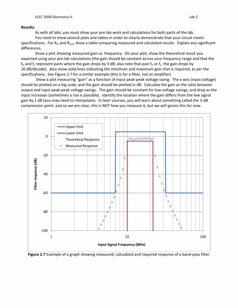
Show a plot showing measured gain vs. frequency. On your plot, show the theoretical result you expected using your pre‐lab calculations (the gain should be constant across your frequency range and that the fH and fL represent parts where the gain drops by 3 dB; also note that past fH or fL, the gain drops by 20 dB/decade). Also show solid lines indicating the minimum and maximum gain that is required, as per the specifications. See Figure 2.7 for a similar example (this is for a filter, not an amplifier)
Show a plot measuring “gain” as a function of input peak‐peak voltage swing. The x‐axis (input voltage) should be plotted on a log scale, and the gain should be plotted in dB. Calculate the gain as the ratio between output and input peak‐peak voltage swings. The gain should be constant for low voltage swings, and drop as the input increases (sometimes a rise is possible). Identify the location where the gain differs from the low signal gain by 1 dB (you may need to interpolate). In later courses, you will learn about something called the 1‐dB compression point‐ just so we are clear, this is NOT how you measure it, but we will ignore this for now.
Figure 2.7 Example of a graph showing measured, calculated and required response of a band‐pass filter.
‐100
‐80
‐60
‐40
‐20
0
20
1 10 100
Filter response (dB)
Input Signal Frequency (MHz)
Upper limit
Lower limit
Theoretical Response
Measured Response