mechanical strain and process strain applied to semiconductor device...
DESCRIPTION
Mechanical Strain and Process strain Applied to Semiconductor Device 應用於半導體元件之機械應變及製程應變 研究生: 詹孫戎 指導教授: 劉致為 博士. Outline. Publication List Mechanically Strained-Si NMOSFETs PMOSFETs Mechanically Strained Si/SiGe HBTs Multi-Plane Reflector of RTP Wafer Bonding - PowerPoint PPT PresentationTRANSCRIPT
Project Title
Mechanical Strain and Process strain Applied to Semiconductor Device
應用於半導體元件之機械應變及製程應變
研究生 : 詹孫戎指導教授 : 劉致為 博士

Project Title
Outline
Publication List Mechanically Strained-Si
NMOSFETs PMOSFETs
Mechanically Strained Si/SiGe HBTs Multi-Plane Reflector of RTP Wafer Bonding Process (Local) Strained-Silicon Simulation Conclusions

Project Title
Publication List
Mechanically strained strained-Si NMOSFETs S. Maikap, C.-Y. Yu, S.-R. Jan, M. H. Lee, and C. W. Liu EDL, VOL. 25, NO. 1, JANUARY 2004
Mechanically strained Si/SiGe HBTs F. Yuan, S.-R. Jan, S. Maikap, Y.-H. Liu, C.-S. Liang, and C. W. Liu To be published in IEEE EDL, July, 2004
Comprehensive study of mechanically strained strained-Si PMOSFETs To be submitted to IEEE Trans. ED

Project Title
Mechanically Strained-Si
Low cost Package strain
(a) Schematic diagram of the externally applied mechanical stress on the wafer
(b) the channel is parallel to the azimuthal direction (Θ ) on the Y axis devices and the channel is parallel to the radial direction ( r ) on the X axis devices.

Project Title
Bender design
底座立體圖01
底座立體圖02
墊片立體圖
上蓋立體圖
Project Title
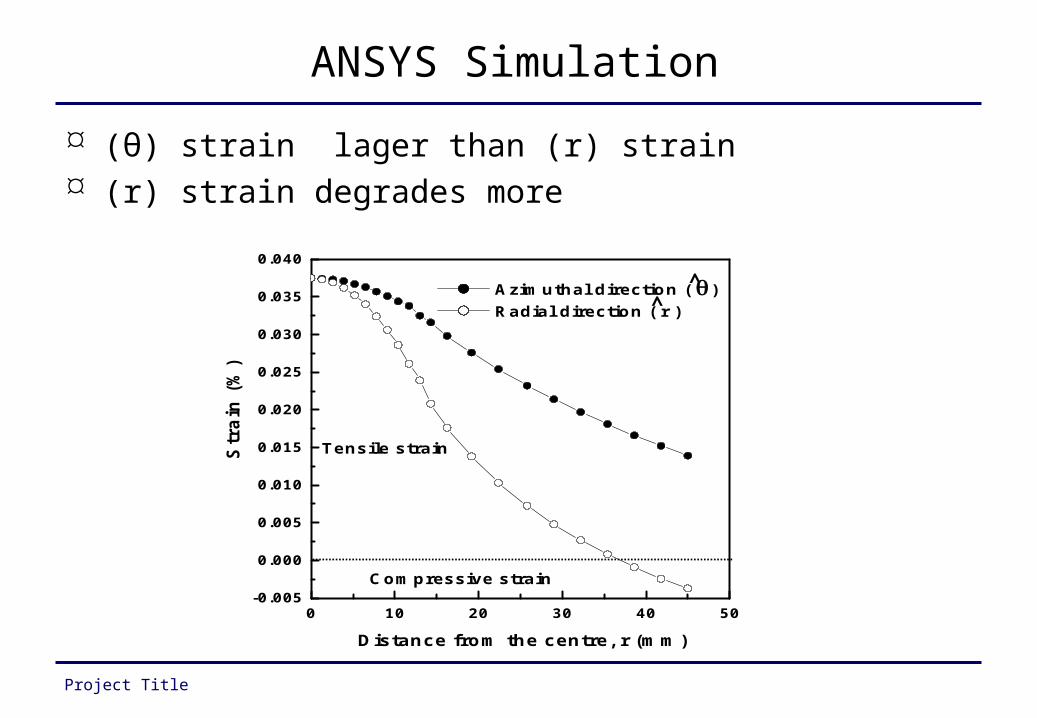
ANSYS Simulation
(θ) strain lager than (r) strain (r) strain degrades more
^^
0 10 20 30 40 50-0.005
0.000
0.005
0.010
0.015
0.020
0.025
0.030
0.035
0.040
Azimuthal direction ( ) Radial direction ( r )
Tensile strain
Compressive strain
Str
ain
(%
)
Distance from the centre, r (mm)

Project Title
Mechanically Strained-Silicon NMOSFETs
• Drain current vs. drain voltages for (a) control Si and strained-Si devices (WxL=25x25 m2) with and without mechanical strain.
0 1 2 30.0
1.0x10⁻⁴
2.0x10⁻⁴
3.0x10⁻⁴
4.0x10⁻⁴
5.0x10⁻⁴
6.0x10⁻⁴
7.0x10⁻⁴
8.0x10⁻⁴
Drain voltage (V)
Dra
in c
urr
ent
(A)
Vgs
-Vt=0 V
Vgs
-Vt=1 V
Vgs
-Vt=2 V
Vgs
-Vt=3 V
w/o stress with stress
(b) Strained-Si

Project Title
Mechanically Strained-Silicon NMOSFETs
Drain current enhancement with the distance from the centre of the wafer for the mechanically strained strained-Si and control Si devices.
0 5 10 15 20 25 30 350
1
2
3
4
5
6
7
Strained-Si
Vgs
-Vt=3.0 V
Vds
=1.0 V
Channel along Channel along r
Control Si
D
rain
cu
rren
t en
han
cem
ent
(%)
Distance from centre (mm)
^^

Project Title
Mechanically Strained-Si PMOSFETs
Drain current vs. drain voltage characteristics of (a) a control Si and (b) a strained-Si PMOSFET devices (WxL=25x0.6 m2) with and without mechanical strain of ~0.087%. The compressive and tensile strains are perpendicular to the channel using the one-end-bending method.
0 -1 -2 -30.0
-3.0x10⁻⁴
-6.0x10⁻⁴
-9.0x10⁻⁴
-1.2x10⁻³
-1.5x10⁻³
-1.8x10⁻³ (a) control Si w/o stress compressive strain (~0.097%) tensile strain (~0.097%)
Vgs
-Vt=-1 V
Vgs
-Vt=-2 V
Vgs
-Vt=-3 V
Dra
in c
urr
ent
(A)
Drain voltage (V)
0 -1 -2 -3
(b) strained-Si compressive strain (~0.097%) tensile strain (~0.097%) w/o stress
Vgs
-Vt=-1 V
Vgs
-Vt=-2 V
Vgs
-Vt=-3 V

Project Title
Effective Mess of Hole
Effective mass (meff) vs. uni-axial and bi-axial strain. Initially it is
assumed that the heavy hole (mhh) = 0.54mo and light hole (mlh) =
0.5mo, where mo = 9.11x10⁻³¹ kg.
-0.10 -0.05 0.00 0.05 0.10-40
-30
-20
-10
0
10
20
30
40assume the initial m
eff of
heavy hole (mhh
)=0.54mo
light hole (mlh)=0.5m
o
mt
mt
ml
tensile compressive
ml
bi-axial
bi-axial
effe
ctiv
e m
ass,
mef
f (%
)
strain(%)

Project Title
Mechanically Strained Si/SiGe HBTs
The Gummel plot of the SiGe HBT device without and with mechanical stress (strain ~0.028%). The base-collector bias is zero volts. (a) is the collector current and (b) is the base current.
(V)
(A) IC-V
BE
0.751x10⁻⁴
3x10⁻⁴
4x10⁻⁴
5x10⁻⁴
w/o stress compressive tensile
0.8
2x10⁻⁴
(A)
(V)
1x10⁻⁶
0.75
2x10⁻⁶
w/o stress compressive tensile
0.8
3x10⁻⁶
5x10⁻⁷
IB-V
BE
13mm from the center(θ) strain ~0.033%( r ) strain ~0.028%Average biaxial strain 0.028%

Project Title
Experiment
The common emitter output characteristics with the constant base current. The SiGe HBT device with compressive mechanical stress has larger output IC than that without mechanical stress.
0.0 0.5 1.0 1.50.0
0.1
0.2
0.3
0.4
0.5
0.6
0.7
0.8
0.9
IB = 2, 4 A
SiGe HBT w/o stress compressive strain (~0.028%) tensile strain (~0.028%)
VCE
(V)
I C (
mA
)

Project Title
Multi-Plane Reflector of RTP
Arrangement of multi-plane reflector, lamp, and wafer. High reflection on the side of reflector to compensate the radiation
loss at the edge.180mm
60mm (ll2)
2mm
4" wafer
lamp
multi-plane reflector
h
h_low_reflectorh_high_reflector

Project Title
Multi-Plane Reflector Simulation
Increase the bonder temperature uniformity for 4 in full wafer bonding
32.542828
1.948212
tot x( )
dir x( )
ref x( )
tot1x( )
32020 x50 0 50 100 150 200 250 300 350
0
5
10
15
20
25
30
35
ψdir(x)
ψtot(x)
ψref(x)
ψdir(x) is the irradiation intensity from the lamps.ψref(x) is the irradiation intensity from the reflector.ψtot(x) is total irradiation intensity [ =ψdir(x) + ψref(x) ]

Project Title
Multi-Plane Reflector design
factors in simulation
2-dimension drafting of multi-plane reflector
Factorsreflector length
ll2 h w h_low_reflector h_high_reflector
Unit (mm) 180 60 40 20 6 8

Project Title
Multi-Plane Reflector design
3-dimension drafting of multi-plane reflector

Project Title
Wafer Bonding design
Spacer
Pressure device
Alignment device
3-dimension drafting of bonder

Project Title
Wafer Bonding Process
(a) Wafer alignment.
(b) Set pressure device.
(c) Apply pressure.
(d) Remove spacer.
•To have one initial contact and have only one bonding wave
•Bonding on full wafer without defects are possible

Project Title
IR-Viwer
IR-viewer Home made: 0.2 M NT Commercial: 1M NT
IR-Viwer IR-bulb

Project Title
Experiment
SOI, GOI applications
Wafer 1
Wafer 2
Defects due to clean room particle
Project Title
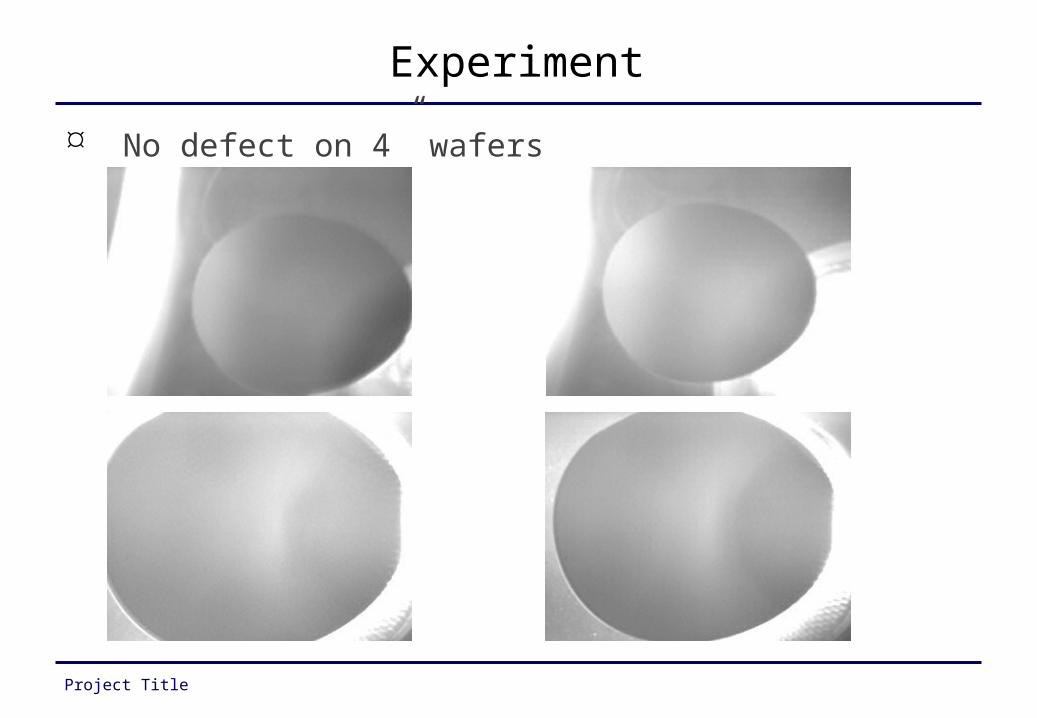
Experiment
No defect on 4” wafers

Project Title
Process (Local) Strained-Silicon Simulation
Introduction Why use strained-Si
because of physical size shrinking limitation Need higher mobility μ
Strained-Si Substrate (global) strained-Si Process (Local) strained-Si
oxt T / )V-(V
charge mobility I
Project Title
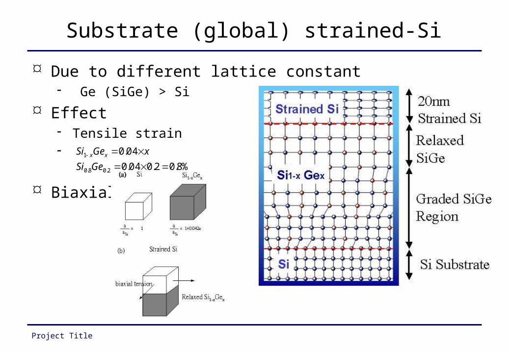
Substrate (global) strained-Si
Due to different lattice constant Ge (SiGe) > Si
Effect Tensile strain
Biaxial
%8.02.004.0
04.0
2.08.0
1
GeSi
xGeSi xx

Project Title
Process (Local) strained-Si
Strain effect
Schematic view of 3D process-induced strain components.
εx is strain in the x directionεy is strain in the y directionεz is strain in the z direction
Direction of Strain Change
CMOS Performance Impact
NMOS PMOS
X Improve Degrade
Y Improve Improve
Z Degrade Improve
•Impact of 3D Strain Effects on CMOS Performance.•Strain change = Increased tensile or decreased compressive strain

Project Title
Process (Local) strained-Si ( Intel’s prescot CPU)
Cap-Layer: Ni4Si3 cap
STI: shallow trench insulator Source/Drain: silicide ; CoSi2 ; TiSi2 ; SiGe
Intel 2003 IEDM Intel 2003 IEDMTSMC 2003 IEDM

Project Title
Simulation
Model Thermal expansion ?
Ni4Si3 Si SiO2
thermal expansion coefficient 4E -6 2.6E -6 0.55E -6Young's modulus ( Pa ; Nt/m2 ) 310G 150G 73GPoisson ratio 0.27 0.28 0.17
MOS structure simulated by ANSY
x

Project Title
ANSYS Simulation
stress is too small εx 0.04%≒ Process strain → 0.4%
Enlarged figure of Fig. 5-2 .The origin of x axis is at the right edge of oxide.
x 0
0 10 20 30 40 50-0.01
0.00
0.01
0.02
0.03
0.04
0.05
0.06
0.07
0.08
stra
in in
the
x d
ire
ctio
n (
%)
X (nm)
y=0.1 nm (below gate oxide) nitride

Project Title
Initial Stress
P-SiN: Plasma-CVD Silicon Nitride
=> compress stress T-SiN: Thermal-CVD Silicon Nitride
=> tensile stress

Project Title
ISE Simulation
Model .25μm MOS Initial stress: 1G
Intel 2003 IEDM
Source Drain
Gate
Nitride
•MOS structure simulated by ISE. •Channel length = 0.25 μm.
Project Title
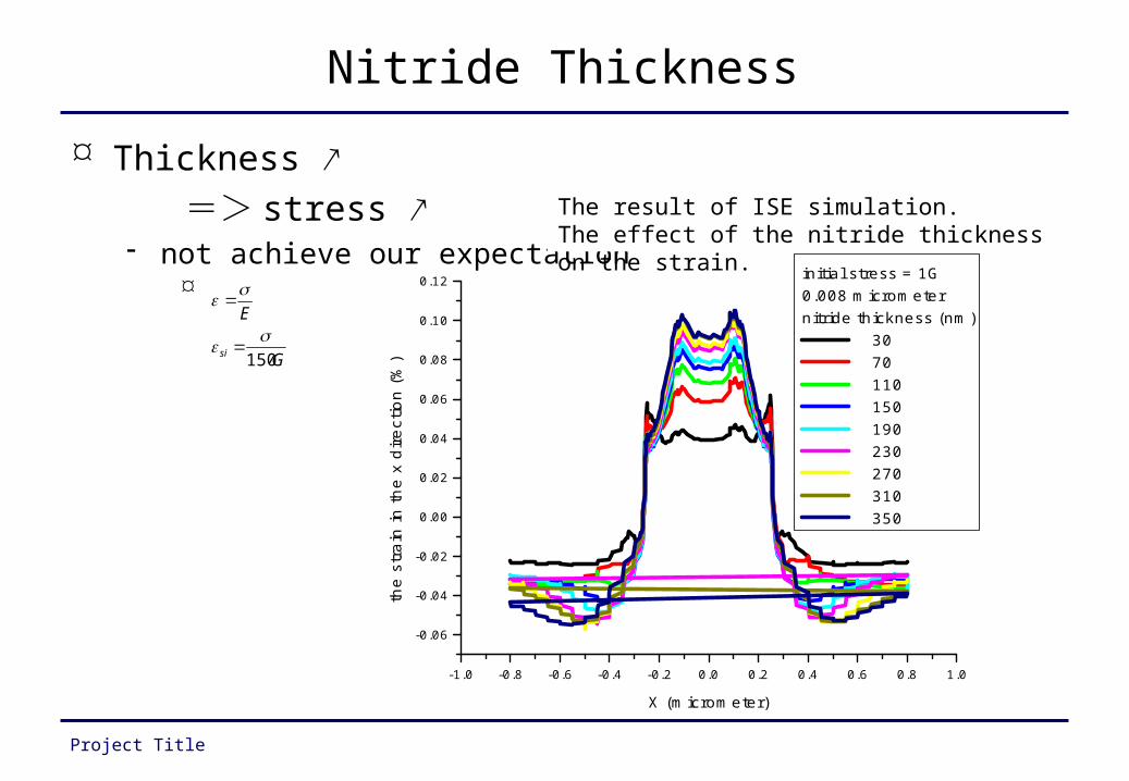
Nitride Thickness
Thickness ↗
=> stress ↗ not achieve our expectation
G
E
si 150
-1.0 -0.8 -0.6 -0.4 -0.2 0.0 0.2 0.4 0.6 0.8 1.0
-0.06
-0.04
-0.02
0.00
0.02
0.04
0.06
0.08
0.10
0.12
the
stra
in in
the
x d
irec
tion
(%)
X (micrometer)
initial stress = 1G0.008 micrometernitride thickness (nm)
30 70 110 150 190 230 270 310 350
The result of ISE simulation.The effect of the nitride thickness on the strain.

Project Title
Nitride Thickness
250nm→0.1% 70nm→0.038%
0 50 100 150 200 250 300 350 400
0.04
0.05
0.06
0.07
0.08
0.09
0.10
the
str
ain
in th
e m
iddl
e o
f th
e ch
an
nel(
%)
the thickness of nitride (nm)
initial stress = 1G
•The result of ISE simulation.•The effect of the nitride thickness on the strain in the middle of channel.

Project Title
Spacer
Intel spacer : sandwich
Enlarged figure of Fig. 5-5.The nitride spacer no sandwich structure.Channel length = 0.25 μm.
Source Drain
Gate
Nitride
(μ m)
Spacer with sandwich structure.Channel length = 0.25 μm.
Source Drain
Gate
Nitride
Oxide
(μ m)

Project Title
The result of ISE simulation.The effect of the sandwich spacer structure on the strain. s channel : the stress of sandwich spacer in the channel.s nitride : the stress of sandwich spacer in the nitride cap.c channel : the stress of control spacer in the channel.c nitride : the stress of control spacer in the nitride cap.
Spacer
Lager stress Sandwich:0.046% Control:0.038%
-0.4 -0.2 0.0 0.2 0.4
-8.00E+007
-6.00E+007
-4.00E+007
-2.00E+007
0.00E+000
2.00E+007
4.00E+007
6.00E+007
8.00E+007
1.00E+008
1.20E+008
1.40E+008
1.60E+008
1.80E+008
stre
ss in
the
x d
ire
ctio
n (
Pa
)
X Axis (micrometer)
s channel s nitride c channel c nitride

Project Title
shrink
.25μm → 50nm Larger stress
50nm ε 0.08%≒
50nm sandwich ε 0.17%≒
MOS structure simulated by ISE.Spacer with sandwich structure.Channel length = 50 nm.
Source Drain
Gate
Nitride
(μ m)
Oxide

Project Title
The result of ISE simulation.The effect of the shrinking dimension on the strain.
shrink
Larger stress 50nm
ε 0.08%≒
50nm sandwich ε 0.17%≒
-0.4 -0.2 0.0 0.2 0.4-1.00E+008
-5.00E+007
0.00E+000
5.00E+007
1.00E+008
1.50E+008
2.00E+008
2.50E+008
stre
ss in
the
x d
ire
ctio
n (
Pa
)
X (micrometer)
channel length 50nm stress in the channel sandwich spacer 50nm stress in the nitride sandwich spacer .25 micrometer stress in the channel .25 micrometer stress in the nitride 50nm stress in the channel 50nm stress in the nitride

Project Title
Conclusions
Mechanically Strained-Si
Multi-Plane Reflector designed and experiment Wafer Bonding : No defect on 4” wafers Process (Local) strained-Si
Initial stress P-SiN: Plasma-CVD Silicon Nitride => compress stress T-SiN: Thermal-CVD Silicon Nitride => tensile stress
Nitride thickness ; sandwich spacer ; size shrink Result lager stress
Tensile strain NMOS PMOS
Parallel Improve Degrade
Perpendicular Improve Improve