按按 下以編輯母片標一下以編輯母片標 void … thermal aging ... factor analysis...
TRANSCRIPT

IEEE Components, Packaging and Manufacturing Technology, SCV Chapter
9/24/2015
www.cpmt.org/scv/1
按一下以編輯母片標Void Formation Void Formation 按 下以編輯母片標題樣式
按一下以編輯母片副標題樣式
Void Formation During SolderingVoid Formation
During Soldering
IEEE/CPMT Lunch MeetingIEEE/CPMT Lunch MeetingSeptember 24, 2015September 24, 2015
Watson Watson TsengTsengGeneral ManagerGeneral Manager
SHENMAO SHENMAO America IncAmerica [email protected][email protected]
OverviewOverview
Two Main Issues in Assembly
Something About Voids
Industrial Standards
Factor Analysis for Void Formation* Surface Finish
* Voids from PCB Design
* Voids from Component
* Voids from Solder Paste
* V id f P
SHENMAOSHENMAOYour Ultimate Choice for Solder
* Voids from Process
Voids in Bumping Process
Conclusion

IEEE Components, Packaging and Manufacturing Technology, SCV Chapter
9/24/2015
www.cpmt.org/scv/2
1. HoP (Head-on-Pillow) and NWO (Non-Wetting Open)
Two Main Issues in AssemblyTwo Main Issues in Assembly
2. Voids in solder joints (not only BGA)
HoP
SHENMAOSHENMAOYour Ultimate Choice for Solder
Types of Voids Description
Macrovoids Voids were formed as volatile ingredients of the fluxes within thesolder paste, usually found everywhere in solder joint.
Planar Voids generated by anomalies in surface finish applicationll l t d i l d f d t th ld t
Something about VoidsSomething about Voids
Microvoids process, generally located in one plane and found at the solder-to-land interface.
Shrinkage Voids Caused by the solidification of SAC solders, formed as linearcracks with rough edges from the surface of the solder joints.
Micro-via Voids Caused by microvias in lands.
Pinhole Voids Voids generated by excursions in the copper plating process atboard supplier.
SHENMAOSHENMAOYour Ultimate Choice for Solder
R. Aspandiar, SMTA Northwest Chapter Meeting (2005)

IEEE Components, Packaging and Manufacturing Technology, SCV Chapter
9/24/2015
www.cpmt.org/scv/3
Something about VoidsSomething about Voids
Kirkendall Voids
During thermal aging (including temp. cycling), rapid diffusion of one material into another could cause crystal vacancies to form in the bulk material, that then leads to risks for reliability failures of solder joints. y j
SAC
Cu Cu
SAC
Cu3Sn
Cu6Sn5
Cu
SAC
Cu3Sn
Cu6Sn5
Kirdendall voids were formed in the Cu3Sn because
SHENMAOSHENMAOYour Ultimate Choice for Solder
3
the Sn and Cu atoms diffused.
During high temperature storage, two IMCs Cu6Sn5
and Cu3Sn continued to grow and a certain amount of solder matrix was the different composition between the voids and neighbor IMCs.
Luhua Xu et al. / Electronics Packaging Technology Conference, IEEE(2005)863–867
Zequn Mei et al. / Electronic Components and Technology Conference, IEEE(2005)415–420
Poor Heat Transfer Rate
Poor Current Carrying Capability
Something about VoidsSomething about Voids
Why don’t we like void?
Long-term Reliability Concern
Squeezed Short
Bump Height Uniformity
SHENMAOSHENMAOYour Ultimate Choice for Solder

IEEE Components, Packaging and Manufacturing Technology, SCV Chapter
9/24/2015
www.cpmt.org/scv/4
Inspection methods of VoidsInspection methods of Voids
Cross-sectionX-Ray CT Scan
Modern 2D/3D X-Ray inspection systems are powerful tools for finding defects in BGA,
2D/3D X-ray CT Scan Cross Section
Resolution
Preparation time
SHENMAOSHENMAOYour Ultimate Choice for Solder
finding defects in BGA, QFN and 3D packages. Analysis time
Automation
Void Location
Accuracy
Cost
Best
Worst
Moderate
Inspection methods of VoidsInspection methods of Voids
SMT System Wafer Bumping System
Voiding Inspection Systems in SHENMAO Lab
Wafer printerPrinter
Dage 7600NT
SHENMAOSHENMAOYour Ultimate Choice for Solder
Reflow oven
X‐ray inspection
Reflow oven

IEEE Components, Packaging and Manufacturing Technology, SCV Chapter
9/24/2015
www.cpmt.org/scv/5
Industrial Standards for VoidsIndustrial Standards for Voids
Component Criteria Standard
Solder Balls of BGA components < 15% JESD 217(Pre‐SMT)
Surface Mount Area Array (Post‐SMT)
< 25% IPC‐A‐610
QFN, MOSFET, Components with Bottom Thermal Plane Terminations
No industrial standard but often target at < 25%
‐
SHENMAOSHENMAOYour Ultimate Choice for Solder
(Post‐SMT)g
Occurrence Rate of VoidsOccurrence Rate of Voids
12% 88%2009
SHENMAO Customer Service Case Studies
40%
30%
13%
35%
25%
13%
20%
25%
45%
74%
80%
2013
2012
2011
2010
SHENMAOSHENMAOYour Ultimate Choice for Solder
30% 50% 20%
0% 20% 40% 60% 80% 100%
2014
MOSFET QFN BGA

IEEE Components, Packaging and Manufacturing Technology, SCV Chapter
9/24/2015
www.cpmt.org/scv/6
Factor Analysis Factor Analysis of Void Formationof Void Formation
C t i ti
Surface Finish
ComponentSolder paste
Contamination
Cleanness
Powder Size
Printing
Void
Surface Finish
DesignActivator
Powder Oxidation
SHENMAOSHENMAOYour Ultimate Choice for Solder
PCB
Reflow Profile
Process
Pad Design Reflow Atmosphere
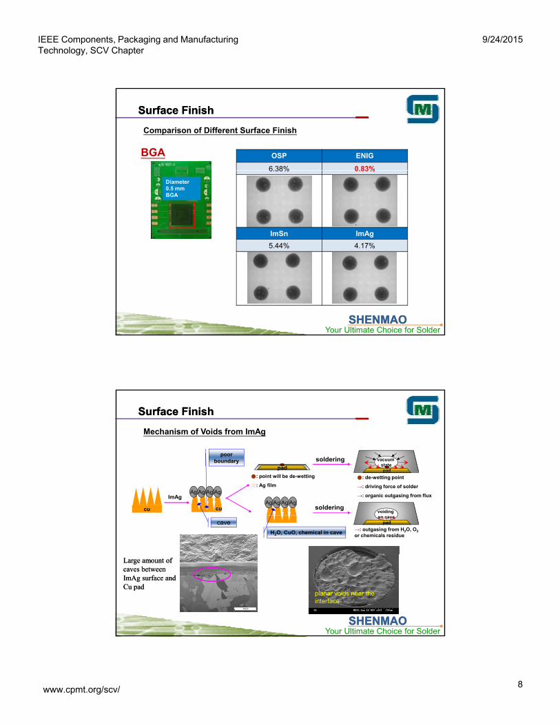
Test Conditions Surface treatment:
OSP / ENIG / ImAg / ImSn
Surface FinishSurface Finish
Pitch 0 4 mm
0603 Chip
RSS profile
OSP / ENIG / ImAg / ImSn
Printer:Panasonic SP18P-L
Stencil thickness:0.12 mm
# of reflow zones:12
Atmosphere:
SHENMAOSHENMAOYour Ultimate Choice for Solder
0.4 mm QFP
Diameter 0.5 mm BGA
air
Heating profile:RSS
Observation Apparatus:MSX2000 X-ray detector

IEEE Components, Packaging and Manufacturing Technology, SCV Chapter
9/24/2015
www.cpmt.org/scv/7
OSP ENIG
2.92% 0.83%
QFP
Comparison of Different Surface Finish
Surface FinishSurface Finish
2.92% 0.83%
ImSn ImAg
2.72% 1.20%
Pitch 0.4 mm QFP
SHENMAOSHENMAOYour Ultimate Choice for Solder
0603 Chip
0603 Chip
OSP ENIG
5.58% 1.54%
Comparison of Different Surface Finish
Surface FinishSurface Finish
0603 Chip 5.58% 1.54%
ImSn ImAg
5.16% 3.37%
SHENMAOSHENMAOYour Ultimate Choice for Solder
IEEE Components, Packaging and Manufacturing Technology, SCV Chapter
9/24/2015
www.cpmt.org/scv/8
BGA OSP ENIG
6.38% 0.83%
Comparison of Different Surface Finish
Surface FinishSurface Finish
Diameter 0.5 mm BGA
6.38% 0.83%
ImSn ImAg
5.44% 4.17%
SHENMAOSHENMAOYour Ultimate Choice for Solder
Mechanism of Voids from ImAg
pad
solderingpoor
boundary vacuum statepad
Surface FinishSurface Finish
●: point will be de-wetting
■: Ag film
AgAgAgAg
H2O, CuO, chemical in cave
cu cu
AgAgAgAg
cave
ImAg
pad
●: de-wetting point
→: driving force of solder
→: organic outgasing from flux
voiding on cave
pad
→: outgasing from H2O, O2
or chemicals residue
soldering
SHENMAOSHENMAOYour Ultimate Choice for Solder
Large amount of Large amount of caves between caves between ImAgImAg surface and surface and Cu padCu pad
planar voids near the interface

IEEE Components, Packaging and Manufacturing Technology, SCV Chapter
9/24/2015
www.cpmt.org/scv/9
Key Factors of Voids from ImSn
DiscolorationLow tin thickness Ionic / organic
Surface FinishSurface Finish
contaminationNG
*Oxidation on ImSn surface
*Transform to IMC layer Dewetting
*De-wetting
De-wetting pointIMC is not good IMC is not good i i h ldi i h ld
SHENMAOSHENMAOYour Ultimate Choice for Solder
Sn
Cu6Sn5
Cu3Sn
Cu
g pwetting with solderwetting with solder
Surface FinishSurface Finish
Cracks from Planar Voids
SHENMAOSHENMAOYour Ultimate Choice for Solder

IEEE Components, Packaging and Manufacturing Technology, SCV Chapter
9/24/2015
www.cpmt.org/scv/10
Poor filling from stencil printing Risk of residue from electroplating
Voids from PCB DesignVoids from PCB Design
Via Hole
Typical Microvia Void
SHENMAOSHENMAOYour Ultimate Choice for Solder
Traces of flying pin test
Voids from ComponentVoids from Component
Contaminations
A very large void in center of the BGA ball
SHENMAOSHENMAOYour Ultimate Choice for Solder
y g
“Balloon effect“ to form large void
gas expansionfrom the pin hole

IEEE Components, Packaging and Manufacturing Technology, SCV Chapter
9/24/2015
www.cpmt.org/scv/11
Two voiding types can be found in MOS, LGA, or any component with larger soldering area
MOS
0. Ideal
Voids from ComponentVoids from Component
1. Gas
MOS
Substrate/PCB
MOS
Substrate/PCB
MOS
Substrate/PCB
MOS
Substrate/PCB
The outer area of the paste will melt firstand then block the inner gas to escape
SHENMAOSHENMAOYour Ultimate Choice for Solder
MOS
Substrate/PCB
2. Non-wettingMOS
Substrate/PCB
Substrate/PCBSubstrate/PCB
MOS
Substrate/PCBThe minimal soldering with the component is caused by non-wetting.
Combination of 2 effects
Two types of voids can be found in MOS or LGA, larger soldering area
1. Gas
Voids from ComponentVoids from Component
2. Non-wetting
SHENMAOSHENMAOYour Ultimate Choice for Solder
Irregular Shape

IEEE Components, Packaging and Manufacturing Technology, SCV Chapter
9/24/2015
www.cpmt.org/scv/12
Take QFN for example
Ground Pad: Ground Pad: Ground Pad:
Voids from ComponentVoids from Component
Stencil Design
Ground Pad:Four-grid
Ground Pad:Nine-grid
Ground Pad:Minus 20% Area
SHENMAOSHENMAOYour Ultimate Choice for Solder
Good: “Window paning” creates vents that results in smaller voids.Bad: Vent channels resulted in additional “open” areas that reduced solder
joint continuity. However, it can’t eliminate voids completely due to the surface finish wetting issues.
large void size small void size minimized void size
Voids from Solder PasteVoids from Solder Paste
Solder paste plays an important role in contribution of void.
High volume of flux High volume of gas generated
Large surface area from solder powder Large surface area from solder powder
Rapid chemical reaction in reflow
Water soluble solder pastes tend to cause larger void than no-clean
ones.
Different chemical compound in flux
SHENMAOSHENMAOYour Ultimate Choice for Solder
Different chemical compound in flux
Moisture absorption

IEEE Components, Packaging and Manufacturing Technology, SCV Chapter
9/24/2015
www.cpmt.org/scv/13
Reflow SimulatorReflow Simulator
Camera 1 (top view) Customized Reflow Profile
Customized Atmosphere (Air/N2)
Monitors what is happening during
C 2 ( id i )
Monitors what is happening during
reflow.
Displays two images at the same time
by connecting two sets of CCD cameras.
Measures the warp caused by thermal
stress Bumping
SHENMAOSHENMAOYour Ultimate Choice for Solder
Reflow chamberCamera 2 (side view)
BGA-1 BGA-2
Flux cleans oxide (gas 1)and activator (gas 2) and
solvent (gas 3) to generate void
Gas may be trapped because of the surface tension
of flux and solder
Mechanism of Void Formation in Reflow
Voids from Solder PasteVoids from Solder Paste
Flux clean tin oxide
SnO2
Flux
Substrate/PCB
VoidSubstrate/PCB
Void
Acid B
Acid CHalide
Acid A
SHENMAOSHENMAOYour Ultimate Choice for Solder
Substrate/PCB
MOMO + R-COOH→ (R-COO-)M + H2O(g)
Flux cleans oxide (gas 1)
R-COOH + R’OH→ R’-COOR + H2O(g)Activator (gas 2)

IEEE Components, Packaging and Manufacturing Technology, SCV Chapter
9/24/2015
www.cpmt.org/scv/14
Ave. 0.19%Max. 1.20%
Powder Size Effect
Voids from Solder PasteVoids from Solder Paste
Substrate
Type 5(15-25μm)
Smaller Surface AreaLess Flux Reaction
Less Gas Generation
L S f A
Ave. 9.64%Max. 13.20%
SHENMAOSHENMAOYour Ultimate Choice for Solder
SubstrateType 7
(2-12μm)
Larger Surface AreaMore Flux Reaction
More Gas Generation
Sample Oxygen content A
Powder Oxidation Effect oxide↓
Ave. 0.92%Max. 2.70%
Voids from Solder PasteVoids from Solder Paste
According to the reaction, the more oxidation on the surface, th H O f ti
A 334 ppm
B 507 ppm
oxide↓
B
SnOx + RCOOH→ (RCOO)ySn + H2O(g)
Ave. 1.86%Max. 4.90%
SHENMAOSHENMAOYour Ultimate Choice for Solder
the more H2O gas formation, resulting in higher voiding.
Yellowish
IEEE Components, Packaging and Manufacturing Technology, SCV Chapter
9/24/2015
www.cpmt.org/scv/15
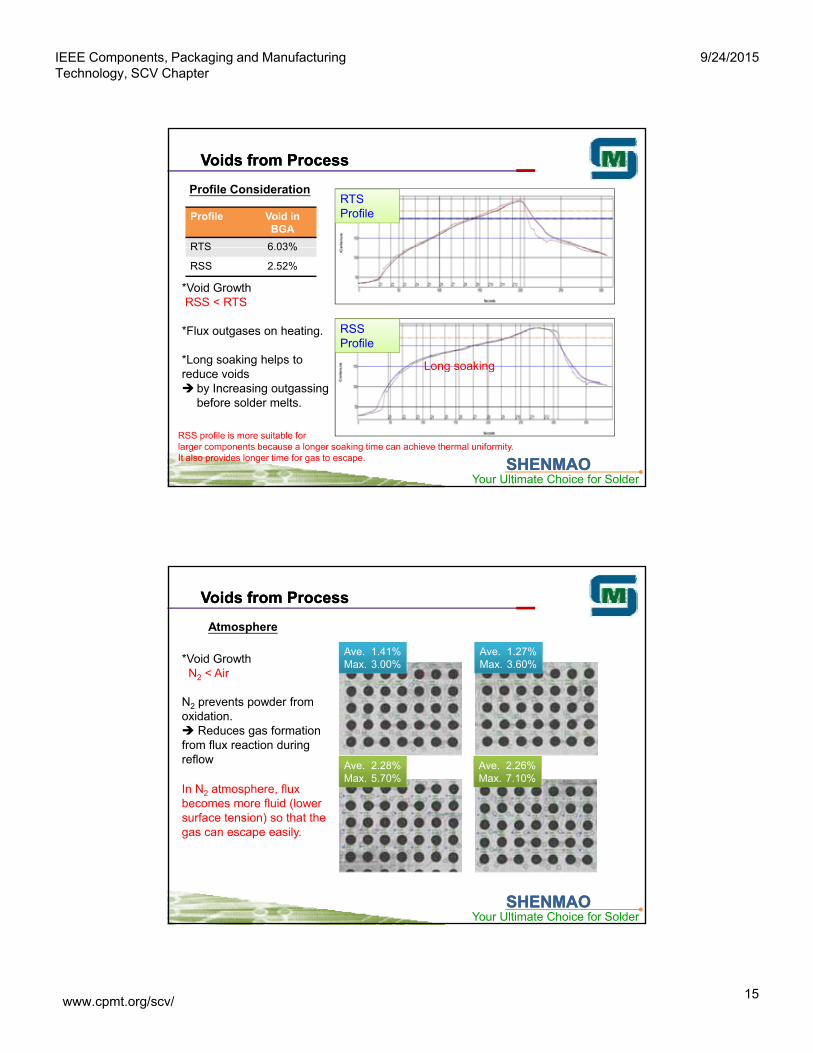
RTS Profile
Voids from ProcessVoids from Process
Profile Consideration
Profile Void in BGA
RTS 6 03%
RSS Profile
Long soaking
*Void GrowthRSS < RTS
*Flux outgases on heating.
*Long soaking helps to
RTS 6.03%
RSS 2.52%
SHENMAOSHENMAOYour Ultimate Choice for Solder
Long soakingreduce voids by Increasing outgassing
before solder melts.
RSS profile is more suitable for larger components because a longer soaking time can achieve thermal uniformity.It also provides longer time for gas to escape.
*Void GrowthN2 < Air
Ave. 1.41%Max. 3.00%
Ave. 1.27%Max. 3.60%
Voids from ProcessVoids from Process
Atmosphere
N2 prevents powder from oxidation. Reduces gas formation from flux reaction during reflow Ave. 2.28%
Max. 5.70%Ave. 2.26%Max. 7.10%
In N2 atmosphere, fluxbecomes more fluid (lower
SHENMAOSHENMAOYour Ultimate Choice for Solder
becomes more fluid (lower surface tension) so that the gas can escape easily.

IEEE Components, Packaging and Manufacturing Technology, SCV Chapter
9/24/2015
www.cpmt.org/scv/16
Vacuum Reflow
Gas evacuates from molten solder easily
Cycle time is 30-60 sec or longer (in-line reflow oven)
Voids from ProcessVoids from Process
Costs much more than conventional reflow oven
Minor risk of splash of flux and solder ball
Minor risk of small sized component shift
Fluxless Reflow (in Formic Acid Atmosphere)
No Flux ≈ No Gas Generation
SHENMAOSHENMAOYour Ultimate Choice for Solder
No Flux ≈ No Gas Generation
Cycle time
Limited cleaning and reduction ability
Solder balls need to be fixed in (ball attach / bumping / pre-solder) process
Voids in Bumping ProcessVoids in Bumping Process
Flux spray
Bumping Solder Paste 2nd reflow Flux Flux clean solvent
Bumping Process
Dry Film
Opening definition Paste deposition
Dry
Film
1st reflow & Dry film removal Flux dispensing 2nd reflow
Flip ChipWafer Bumping
Flip Chip Tacky Flux Substrate Bumping
SHENMAOSHENMAOYour Ultimate Choice for Solder
基板Substrate
PCB
BGA Flux
SMT Solder Paste

IEEE Components, Packaging and Manufacturing Technology, SCV Chapter
9/24/2015
www.cpmt.org/scv/17
Voids in Bumping ProcessVoids in Bumping Process
Voids are big challenges for bumping process
Problem from Production Process
Problem from Wafer/Substrate
Bad printing
condition
reflow condition
Plating liquid
residue
Poor wetting
and oxidation on pad
Shape design of dry film
SHENMAOSHENMAOYour Ultimate Choice for Solder
Excess (high) melting
temperature and meting
time
Excess (high) speed heating in secondary heating zone
Thick printingMoisture
Voids in Bumping ProcessVoids in Bumping Process
Solder Paste Design
Flux Conventional New Formula
Rosin 20~50% R1 R1
Activator 0~10% A1+A2 A1+A2+A3 activity in fluxHalide 0~5% H1 H2
Thixotropic 0~10% T1 T2
Solvent 10~25% S1+S2 S2+S3
ConventionalAve. 3.04%Max. 7.40%
y
thixotropic property
viscosity
In-house testing results (piece wafer)
SHENMAOSHENMAOYour Ultimate Choice for Solder
New FormulaAve. 1.03%Max. 3.90%

IEEE Components, Packaging and Manufacturing Technology, SCV Chapter
9/24/2015
www.cpmt.org/scv/18
Voids in Bumping ProcessVoids in Bumping Process
Wafer Type Dummy Dummy
Solder Paste Design
In-Line Testing Results (Full Wafer)
Paste Conventional New Formula
Dry Film Opening (μm) 150 150
FV bump id (%)
Sample Size 7500 7500
> 30 1 0
26-30 8 4
21-25 31 10
16-20 56 16
SHENMAOSHENMAOYour Ultimate Choice for Solder
void (%)16 20 56 16
11-15 113 9
Amount Void 209 39
Void Rate (%) 2.78 0.52
Max Void Size 31% 30%
Voids in Bumping ProcessVoids in Bumping Process
1 2 3 4 5
Solder Paste Design
New Formula
650
700
750
800
gth
(m
N) New
Conventional
Shear Strength
Shear strength of solder bump increased because of low voiding from new solder paste formula
SHENMAOSHENMAOYour Ultimate Choice for Solder
400
450
500
550
600
0 1 2 3
Sh
ea
r S
tre
ng
Reflow
Shear strengths dropped after multiple reflow.
from new solder paste formula.

IEEE Components, Packaging and Manufacturing Technology, SCV Chapter
9/24/2015
www.cpmt.org/scv/19
ConclusionConclusion
Design
1. Select a suitable surface finish.
2. Choose right solder powder size.g p
3. Avoid microvia.
4. Design stencil aperture properly for large ground pad.
Process
1. Control the quality of incoming component and PCB. Low cost is
not always the best!
SHENMAOSHENMAOYour Ultimate Choice for Solder
2. Discuss with solder paste manufacturer for best reflow profile. Or
try different soldering paste.
3. Use Nitrogen reflow or Vacuum reflow if possible.
Thank you!Thank you!
SHENMAOSHENMAOYour Ultimate Choice for Solder