10.1.1.62.5808
TRANSCRIPT

8/7/2019 10.1.1.62.5808
http://slidepdf.com/reader/full/1011625808 1/20
A Scalable and Unified Multiplier Architecture
for Finite Fields GF (p) and GF (2
m
)
∗†‡
E. Savas, A. F. Tenca, and C. K. KocElectrical & Computer Engineering
Oregon State UniversityCorvallis, Oregon 97331
Abstract
We describe a scalable and unified architecture for a Montgomery multiplication module
which operates in both types of finite fields GF (p) and GF (2m
). The unified architecture re-quires only slightly more area than that of the multiplier architecture for the field GF (p). Themultiplier is scalable, which means that a fixed-area multiplication module can handle operandsof any size, and also, the wordsize can be selected based on the area and performance require-ments. We utilize the concurrency in the Montgomery multiplication operation by employing apipelining design methodology. We also describe a scalable and unified adder module to carryout concomitant operations in our implementation of the Montgomery multiplication. The up-per limit on the precision of the scalable and unified Montgomery multiplier is dictated only bythe available memory to store the operands and internal results, and the module is capable of performing infinite-precision Montgomery multiplication in both types of finite fields.
Key Words: Prime fields, binary extension fields, multiplication, Montgomery multiplication,scalability, hardware implementation.
1 Introduction
The basic arithmetic operations (i.e., addition, multiplication, and inversion) in prime and binaryextension fields, GF (p) and GF (2m), have several applications in cryptography, such as decipher-ment operation of RSA algorithm [18], Diffie-Hellman key exchange algorithm [3], elliptic curvecryptography [7, 12], and the Digital Signature Standard including the Elliptic Curve DigitalSignature Algorithm [15]. The most important of these three arithmetic operations is the fieldmultiplication operation since it is the core operation in many cryptographic functions.
The Montgomery multiplication algorithm [13] is an efficient method for doing modular mul-tiplication with an odd modulus. The Montgomery multiplication algorithm is a very useful for
obtaining fast software implementations of the multiplication operation in prime fields GF (p). Thealgorithm replaces division operation with simple shifts, which are particularly suitable for im-plementation on general-purpose computers. The Montgomery multiplication operation has been
∗Cryptographic Hardware and Embedded Systems - CHES 2000 , C. K. Koc and C. Paar, editors, Lecture Notes
in Computer Science No. 1965, pages 281-296, Springer Verlag, Berlin, Germany, 2000.†The reader should note that Oregon State University has filed US and International patent applications for
inventions described in this paper.‡This work is supported by Secured Information Technology, Inc.
1

8/7/2019 10.1.1.62.5808
http://slidepdf.com/reader/full/1011625808 2/20
extended to the finite field GF (2k) in [9]. Efficient software implementations of the multiplica-tion operation in GF (2k) can be obtained using this algorithm, particularly when the irreduciblepolynomial generating the field is chosen arbitrarily. The main idea of the architecture proposedin this paper is based on the observation that the Montgomery multiplication algorithm for bothfields GF (p) and GF (2k) are essentially the same algorithm. The proposed unified architecture
performs the Montgomery multiplication in the field GF (p) generated by an arbitrary prime p andin the field GF (2m) generated by an arbitrary irreducible polynomial p(x). We show that a unifiedmultiplier performing the Montgomery multiplication operation in the fields GF (p) and GF (2k)can be designed at a cost only slightly higher than the multiplier for the field GF (p), providingsignificant savings when both types of multipliers are needed.
Several variants of the Montgomery multiplication algorithm [17, 10, 2] have been proposedto obtain more efficient software implementations on specific processors. Various hardware im-plementations of the Montgomery multiplication algorithm for limited precision operands are alsoreported [2, 17, 4]. On the other hand, implementations utilizing high-radix modular multipliershave also been proposed [17, 11, 19]. Advantages and disadvantages of using high-radix repre-sentation have been discussed in [22, 21]. Because high-radix Montgomery multiplication designsintroduce longer critical paths and more complex circuitry, these designs are less attractive forhardware implementations.
A scalable Montgomery multiplier design methodology for GF (p) was introduced in [21] in orderto obtain hardware implementations. This design methodology allows to use a fixed-area modularmultiplication circuit for performing multiplication of unlimited precision operands. The designtradeoffs for best performance in a limited chip area were also analyzed in [21]. We use the designapproach as in [21] to obtain a scalable hardware module. Furthermore, the scalable multiplierdescribed in this paper is capable of performing multiplication in both types finite fields GF (p)and GF (2k), i.e., it is a scalable and unified multiplier.
The main contributions of this paper are summarized below.
• We show that a unified architecture for multiplication module which operates both in GF (p)
and GF (2m
) can be designed easily without compromising scalability, time and area efficiency.
• We analyze the design considerations such as the effect of word length, the number of thepipeline stages, and the chip area, etc., by supplying implementation results obtained byMentor graphics synthesis tools.
• We describe the design of a dual-field, scalable adder circuit which is suitable for the pipelineorganization of the multiplier. This adder is necessary for the final reduction step in theMontgomery algorithm and in the final addition for converting the result of the multiplicationoperation (which is in the Carry-Save form) to the nonredundant form. Naturally, the adderoperates both in GF (p) and GF (2m). We give an analysis of the time and area cost of theadder circuit.
We start with a short discussion of scalability in §2 and explain the main idea behind theunified multiplier architecture in §3. We then present the methodology to perform the Montgomerymultiplication operation in both types of finite fields using the unified architecture. We give theoriginal and modified definitions of Montgomery algorithm for GF (p) and GF (2m) in §4. We discussconcurrency in the Montgomery multiplication and show the methodology to design a pipelinemodule utilizing the concurrency in §5. We present the processing unit and the modifications neededto make the unit operate in prime and binary extension fields in §6. We then provide a multi-purpose
2

8/7/2019 10.1.1.62.5808
http://slidepdf.com/reader/full/1011625808 3/20
word adder/subtractor module in §7, which can be integrated into the main Montgomery multipliermodule in order to perform the field addition and subtraction operations. In §8, we discuss thearea/time tradeoffs and suitable choices for word lengths, the number of pipeline stages, and typicalchip area requirements. Finally, we summarize our conclusions in §9.
2 Scalable Multiplier Architecture
An arithmetic unit is called scalable if it can be reused or replicated in order to generate long-precision results independently of the data path precision for which the unit was originally designed.To speed up the multiplication operation, various dedicated multiplier modules were developed in[19, 1, 14]. These designs operate over a fixed finite field. For example, the multiplier designed for155 bits [1] cannot be used for any other field of higher degree. When a need for a multiplicationof larger precision arises, a new multiplier must be designed. Another way to avoid redesigningthe module is to use software implementations and fixed precision multipliers. However, softwareimplementations are inefficient in utilizing inherent concurrency of the multiplication because of the inconvenient pipeline structure of the microprocessors being used. Furthermore, software im-
plementations on fixed digit multipliers are more complex and require excessive amount of effortin coding. Therefore, a scalable hardware module specifically tailored to take advantage of theconcurrency of the Montgomery multiplication algorithm becomes extremely attractive.
3 Unified Multiplier Architecture
Even though prime and binary extension fields, GF (p) and GF (2m), have dissimilar properties, theelements of either field are represented using almost the same data structures inside the computer.In addition, the algorithms for basic arithmetic operations in both fields have structural similar-ities allowing a unified module design methodology. For example, the steps of the Montgomerymultiplication algorithm for binary extension field GF (2m) given in [9] only slightly differs from
those of the integer Montgomery multiplication algorithm [13, 10]. Therefore, a scalable arithmeticmodule, which can be adjusted to operate in both types of fields, is feasible, provided that thisextra functionality does not lead to an excessive increase in area or a dramatic decrease in speed.In addition, designing such a module must require only a small amount of extra effort and no majormodification in control logic of the circuit.
Considering the amount of time, money and effort that must be invested in designing a multipliermodule or more generally speaking a cryptographic coprocessor, a scalable and unified architecturewhich can perform arithmetic in two commonly used algebraic fields is definitely beneficial. In thispaper, we show the method to design a Montgomery multiplier that can be used for both typesof fields following the design methodology presented in [21]. The proposed unified architecture isobtained from the scalable architecture given in [21] after minor modifications. The propagationtime is unaffected and the increase in chip area is insignificant.
4 Montgomery Multiplication
Given two integers A and B, and the prime modulus p, the Montgomery multiplication algorithmcomputes
C = MonMul(A, B) = A · B · R−1 (mod p) , (1)
3

8/7/2019 10.1.1.62.5808
http://slidepdf.com/reader/full/1011625808 4/20
where R = 2m and A, B < p < R, and p is an m-bit number. The original algorithm works forany modulus n provided that gcd(n, R) = 1. In this paper, we assume that the modulus is a primenumber, thus, we perform multiplication in the field defined by this prime number. This issue isalso relevant when the algorithm is defined for the binary extension fields.
The Montgomery multiplication algorithm relies on a different representation of the finite field
elements. The field element A ∈ GF (p) is transformed into another element¯
A ∈ GF (p) using theformula A = A · R (mod p). The number A is called Montgomery image of the element, or A issaid to be in the Montgomery domain. Given two elements in the Montgomery domain A and B,the Montgomery multiplication computes
C = A · B · R−1 (mod p) = (A · R) · (B · R) · R−1 (mod p) = C · R (mod p) , (2)
where C is again in the Montgomery domain. The transformation operations between the twodomains can also be performed using the MonMul function as
A = MonMul(A, R2) = A · R2 · R−1 = A · R (mod p) ,
B = MonMul(B, R2) = B · R2 · R−1 = B · R (mod p) ,
C = MonMul(C, 1) = C · R · R−1 = C (mod p) .
Provided that R2 (mod p) is precomputed and saved, we need only a single MonMul operation tocarry out each of these transformations. However, because of these transformation operations, per-forming a single modular multiplication using MonMul might not be advantageous, however, thereis a method to make it efficient for a few modular multiplications by eliminating the need for thesetransformations [16]. The advantage of the Montgomery multiplication becomes much more ap-parent in applications requiring multiplication-intensive calculations, e.g., modular exponentiationor elliptic curve point operations. In order to exploit this advantage, all arithmetic operations areperformed in the Montgomery domain, including the inversion operation [6, 20]. Furthermore, it isalso possible to design cryptosystems in which all calculations are performed in the Montgomery
domain eliminating the transformation operations permanently.Below, we give bitwise Montgomery multiplication algorithm for obtaining C := ABR−1
(mod p), where A = (am−1, . . . , a1, a0), B = (bm−1, . . . , b1, b0), and C = (cm−1, . . . , c1, c0).
Input: A, B ∈ GF (p) and m = log2 pOutput: C ∈ GF (p)Step 1: C := 0Step 2: for i = 0 to m − 1Step 3: C := C + aiBStep 4: C := C + c0pStep 5: C := C/2Step 6: if C ≥ p then C := C − p
Step 7: return C
In the case of GF (2m), the definitions and the algorithms are slightly different since we use poly-nomials of degree at most m − 1 with coefficients from the binary field GF (2) to represent the fieldelements. Given two polynomials
A(x) = am−1xm−1 + am−2xm−2 + · · · + a1x + a0
B(x) = bm−1xm−1 + bm−2xm−2 + · · · + b1x + b0 ,
4

8/7/2019 10.1.1.62.5808
http://slidepdf.com/reader/full/1011625808 5/20
and the irreducible monic degree-m polynomial
p(x) = xm + pm−1xm−1 + pm−2xm−2 + · · · + p1x + p0
generating the field GF (2m), the Montgomery multiplication of A(x) and B(x) is defined as thefield element C (x) which is given as
C (x) = A(x) · B(x) · R(x)−m (mod p(x)) . (3)
We note that, as compared to Equation (1), R(x) = xm replaces R = 2m. The representation of xm
in the computer is exactly the same as the representation of 2m, i.e., a single 1 followed by 2m zeros.Furthermore, the elements of GF (p) and GF (2m) are represented using the same data structures.For example, the elements of GF (7) for p = 7 and the elements of GF (23) for p(x) = x3 + x + 1are represented in the computer as follows:
GF (7) = {000, 001, 010, 011, 100, 101, 110} ,
GF (23) = {000, 001, 010, 011, 100, 101, 110, 111} .
Only the arithmetic operations acting on the field elements differ. The Montgomery image of apolynomial A(x) is given as A(x) = A(x) · xm (mod p(x)). Similarly, before performing Mont-gomery multiplication, the operands must be transformed into the Montgomery domain and theresult must be transformed back. These transformations are accomplished using the precomputedvariable R2(x) = x2m (mod p(x)) as follows:
A(x) = MonMul(A, R2) = A(x) · R2(x) · R−1(x) = A(x) · R(x) (mod p(x)) ,
B(x) = MonMul(B, R2) = B(x) · R2(x) · R−1(x) = B(x) · R(x) (mod p(x)) ,
C (x) = MonMul(C, 1) = C (x) · R(x) · R−1(x) = C (x) (mod p(x)) .
The bit-level Montgomery multiplication algorithm for the field GF (2m) is given below:
Input: A(x), B(x) ∈ GF (2m), p(x), and m
Output: C (x)Step 1: C (x) := 0Step 2: for i = 0 to m − 1Step 3: C (x) := C (x) + aiB(x)Step 4: C (x) := C (x) + c0p(x)Step 5: C (x) := C (x)/xStep 6: return C (x)
We note that the extra subtraction operation in Step 6 of the previous algorithm is not required inthe case of GF (2m), as proven in [9]. Also, the addition operations are different. While additionin binary field is just bitwise mod 2 addition, the addition in GF (p) requires carry propagation.
Our basic observation is that it is possible to design a unified Montgomery multiplier which canperform multiplication in both types of fields if an adder module, equipped with the property of performing addition with or without carry, is available. The design of an adder with this propertyis provided in the following sections.
The algorithms presented in this section require that the operations be performed using fullprecision arithmetic modules, thus, limiting the designs to a fixed degree. In order to design ascalable architecture, we need modules with the scalability property. The scalable algorithms areword-level algorithms, which we give in the following sections.
5

8/7/2019 10.1.1.62.5808
http://slidepdf.com/reader/full/1011625808 6/20
4.1 The Multiple-Word Montgomery Multiplication Algorithm for GF (p)
The use of fixed precision words alleviates the broadcast problem in the circuit implementation.Furthermore, a word-oriented algorithm allows design of a scalable unit. For a modulus of m-bitprecision, e = m/w words (each of which is w bits) are required. The algorithm proposed in [21]scans the operand B (multiplicand) word-by-word, and the operand A (multiplier) bit-by-bit. The
vectors involved in multiplication operations are expressed as
B = (B(e−1), . . . , B(1), B(0)) ,
A = (am−1, . . . , a1, a0) ,
p = (p(e−1), . . . , p(1), p(0)) ,
where the words are marked with superscripts and the bits are marked with subscripts. For example,
the ith bit of the kth word of B is represented as B(k)i . A particular range of bits in a vector B
from position i to j where j > i is represented as Bj..i. Finally, 0m represents an all-zero vector of m bits. The algorithm is given below:
Input: A, B ∈ GF (p) and p
Output: C ∈ GF (p)Step 1: (T C , T S ) := (0m, 0m)Step 2: (Carry0,Carry1) := (0, 0)Step 3: for i = 0 to m − 1
Step 4: (T C (0), T S (0)) := ai · B(0) + T C (0) + T S (0)
Step 5: Carry0 := T C (0)w−1
Step 6: T C (0) := (T C (0)w−2..0|0)
Step 7: parity := T S 00Step 8: (T C (0), T S (0)) := parity · p(0) + T C (0) + T S (0)
Step 9: T S (0)w−2..0 := T S
(0)w−1..1
Step 10: for j = 1 to e − 1
Step 11: (T C (j), T S (j)) := ai · B(j) + T C (j) + T S (j)
Step 12: Carry1 := T C (j)w−1
Step 13: T C (j)w−1..1 := T C
(j)w−2..0
Step 14: T C (j)0 := Carry0
Step 15: Carry0 := Carry1
Step 16: (T C (j), T S (j)) := parity · p(j) + T C (j) + T S (j)
Step 17: T S (j−1)w−1 := T S
(j)0
Step 18: T S (j)w−2..0 := T S
(j)w−1..1
Step 19: end for
Step 20: T S (e−1)w−1 := 0
Step 21: end forStep 22: C := T C + T S Step 23: if C > p thenStep 24: C := C − pStep 25: return C
As suggested in [21], we use the Carry-Save form in order to represent the intermediate resultsin the algorithm. The result of an addition is stored in two variables ( T C (j), T S (j)), thus, they can
6

8/7/2019 10.1.1.62.5808
http://slidepdf.com/reader/full/1011625808 7/20
grow as large as 2m+1 + 2m − 3 which is exactly equal to the result of the addition of three numbersat the right hand side of equations in Steps 4, 8, 11, and 16. Recall that T C (j) and T S (j) are m-bitnumbers, but T C (j) must be seen as a number multiplied by 2 since it represents the carry vectorin the Carry-Save notation. At the end of Step 21, we obtain the result in the Carry-Save formwhich needs an extra addition to get the final result in the nonredundant form. If the final result
is greater than the modulus p, one subtraction operation must be performed as shown in Step 24.
4.2 Multiple-Word Montgomery Multiplication Algorithm for GF (2m)
The Montgomery multiplication algorithm for GF (2m) is given below. Since there is no carrycomputation in GF (2m) arithmetic, the intermediate addition operations are replaced by bitwiseXOR operations, which are represented below using the symbol ⊕.
Input: A, B ∈ GF (2m) and p(x)Output: C ∈ GF (2m)Step 1: T S := 0m
Step 2: for i = 0 to m
Step 3: T S (0) := aiB(0) ⊕ T S (0)Step 4: parity := T S
(0)0
Step 5: T S (0) := parity · p(0) ⊕ T S (0)
Step 6: T S (0)w−2..0 := T S
(0)w−1..1
Step 7: for j = 1 to e − 1
Step 8: T S (j) := aiB(j) ⊕ T S (j)
Step 9: T S (j) := parity · p(j) ⊕ T S (j)
Step 10: T S (j−1)w−1 := T S
(j)0
Step 11: T S (j)w−2..0 := T S
(j)w−1..1
Step 12: end for
Step 13: T S
(e−1)
w−1 := 0Step 14: end for
Step 15: C := T S Step 15: return C
Notice that in the outer loop the index i runs from 0 to m. Since (m + 1) bits are requiredto represent irreducible polynomial of GF (2m), we prefer to allocate (m + 1) bits to express thefield elements. We can also modify the algorithm for GF (p) accordingly for sake of uniformity.Therefore, the formula for the number of words to represent a field element for both cases is givenas e = (m + 1)/w where w is the selected wordsize.
5 Concurrency in Montgomery MultiplicationIn this section, we analyze the concurrency in Montgomery multiplication algorithms as given inthe subsections §4.1 and §4.2. In order to accomplish this task, we need to determine the inherentdata dependencies in the algorithm and describe a scheme to allow the Montgomery multiplicationto be computed on an array of processing units organized in a pipeline.
We prefer to accomplish concurrent computation of the Montgomery multiplication by exploit-ing the parallelism among the instructions across the different iterations of i-loop of the algorithms,
7

8/7/2019 10.1.1.62.5808
http://slidepdf.com/reader/full/1011625808 8/20
as proposed in [21]. We scan the multiplier one bit at a time, and after the first words of the in-termediate variables (T C , T S ) are fully determined, which takes two clock cycles, the computationfor the second bit of A can start. In other words, after the inner loop finishes the execution forj = 0 and j = 1 in ith iteration of the outer loop, the (i + 1)th iteration of outer loop starts itsexecution immediately. The dependency graph shown in Figure 1 illustrates these computations.
Figure 1: The dependency graph of the MonMul algorithm.
a0
B(1)
p(1)
B(2)
p(2)
p(3)
p(4)
p(5)
p(6)
B(0)
p(0)
B(3)
B(4)
B(5)
B(6)
B(0)
B(0)
p(0)
p(0)
B(1)
B(1)
p(1)
p(1)
B(2)
B(2)
p(2)
p(2)
B(3)
B(4)
p(4)
p(3)
a1
a2
(0,0)
(0,0)
(0,0)
(0,0)
(0,0)
(0,0)
Each circle in the graph represents an elementary computation performed in each iteration of the j-loop. We observe from this graph that these computations are very suitable for pipelining.Each column in the graph represents operations that can be performed by separate processing units(PU) organized as a pipeline. Each PU takes only one bit from multiplier A and operates on eachword of multiplicand, B, each cycle. Starting from the second clock cycle, a PU generates one wordof partial sum T = (T C , T S ) in the Carry-Save form at each cycle, and communicates it to thenext PU which adds its contribution to the partial sum, when its turn comes. After e + 1 clockcycles, the PU finishes its portion of work, and becomes available for further computation. In casethere is no available PU and there is work to do, the pipeline must stall and wait for the workingPUs to finish their jobs. Since the PU at the end of the pipeline has no way of communicating itsresult to another PU, we need to provide extra buffers for them. In the worst case, which happenswhen there is only one PU, there must be 2e extra buffers of w length to hold these partial sum
8

8/7/2019 10.1.1.62.5808
http://slidepdf.com/reader/full/1011625808 9/20
words. In the last clock cycle of each column, the The PU responsible for this column must receivep(e) = B(e) = 0. Elementary computations represented by circles in Figure 1 are performed on the
same hardware module. Local control module in the PU must be able to extract T S (0)0 and keep
this value for the entire operand scanning. Each PU, in other words, has to obtain this value anduse it to decide whether to add the modulus p to the partial sum. This value is determined in the
first clock cycle of the each stage.An example of the computation for 7-bit operands is shown in Figure 2 for the word size w = 1provided that there are sufficient number of PUs preventing the pipeline to stall. Note that thereis a delay of 2 clock cycles between the stage for xi and the stage for xi+1. The total executiontime for the computation takes 20 clock cycles in this example.
Figure 2: An example of pipeline computation for 7-bit operands, where w = 1.
Time (clock cycle)
Stage 1 2 3 4 5 6 7 8 9 10 11 12 13 1415 16 17 18 19 20
1
2
3
5
6
4
7
If there are at least (e + 1)/2 PUs in the pipeline organization the pipeline stalls do not takeplace. For the example in Figure 2, less than 8/2 = 4 PUs cause the pipeline to stall. Figure 3shows what happens if there are only three PUs available for the same example.
Figure 3: An example of pipeline computation for 7-bit operands,
illustrating the situation of pipeline stalls, where w = 1.
Time (clock cycle)
Stage 1 2 3 4 5 6 7 8 9 10111213141516171819202122232425262728
9
1
2
3
5
6
4
8
7
Regular computation
Pipeline Stall
Extra Pipeline Stages Computation
At the clock cycles 7 and 15, the pipeline cannot engage a PU, and thus, it must stall for 2extra cycles. At the 9th and 17th cycles, the first PU becomes available and computation proceeds.
9

8/7/2019 10.1.1.62.5808
http://slidepdf.com/reader/full/1011625808 10/20
We need a buffer of 4-bit length to store the partial sum bits during the stall. Because the 8 isnot a multiple of 3, the last two pipeline stages perform extra computations. Since it is a pipelineorganization, it is not possible to stop the computations at any time. In [21], these extra cycles aretreated as waste cycles. However, it is possible to perform useful computation without complicatingthe circuit. Recall that C = A·B ·2−m (mod p) where m is the number of bits in the modulus p. If
we continue the computations in these extra pipeline cycles, we calculate C = A · B · 2−n
(mod p)where n > m is the smallest integer multiple of the number of PUs in the pipeline organization. Itis always easy to rearrange the Montgomery settings according to this new Montgomery exponent,namely R = 2n, or R = xn for the field GF (2m) case.
The total computation time, CC (clock cycles), is slightly different from the one in [21] and isgiven as
CC =
(m+1
k − 1)2k + e + 1 + 2(k − 1) if (e + 1) < 2k ,
(m+1k
)(e + 1) + 2(k − 1) otherwise ,
where k is the number of PUs in the pipeline. Notice that the first line of the formula givesthe execution time in clock cycles when there are sufficiently many PUs while the second linecorresponds to the case when there are stalls in the pipeline. At certain clock cycles some of the
PUs become idle, and this affects the utilization of the unit, which can be formulated as
U =Total number of clock cycles per bit of A × m
Total number of clock cycles × k=
(e + 1) · m
CC · k.
Figure 4 shows (from left to right) the total execution time CC , the speedup introduced by use of more units over a single unit, and the hardware utilization U for a range of precision. We preferto select the wordsize as w = 32 in order to provide a realistic example, considering that mostmulti-purpose microprocessors have 32-bit datapaths.
Figure 4: The performance of multiple units with w = 32.
0 100 200 3000
500
1000
1500
2000
2500
Modulus Precision (bits)
Time (Clock Cycles)
Total Execution Time
3 PU
2 PU
1 PU
0 100 200 3000.5
1
1.5
2
2.5
3
Modulus Precision (bits)
Speedup
Speedup over a single PU
3 PU
2 PU
0 100 200 3000.1
0.2
0.3
0.4
0.5
0.6
0.7
0.8
0.9
1
Modulus Precision (bits)
Utilization
Utilization
1 PU
2 PU
3 PU
10

8/7/2019 10.1.1.62.5808
http://slidepdf.com/reader/full/1011625808 11/20
6 Scalable Architecture
An example of pipeline organization with 2 PUs is shown in Figure 5. An important aspect of thisorganization is the register file design. The bits of multiplier ai are given serially to the PUs, and arenot used again in later stages and can be discarded immediately. Therefore, a simple shift registerwould be sufficient for the multiplier. The registers for the modulus p and multiplicand B can alsobe shift registers. When there is no pipeline stall, the latches between PUs forward the modulusand multiplicand to next PU in the pipeline. However, if pipeline stalls occur, the modulus andmultiplicand words generated at the end of the pipeline enter the SR − p and SR −B registers. Thelength of these shift registers are of crucial importance and determined by the number of pipelinestages (k) and the number of words (e) in the modulus. By considering that SR − p and SR − Bvalues require one extra register to store the all-zero word needed for the last clock cycle in everystage (recall that p(e) = B(e) = 0) the length of these registers can be given as
L1 =
e + 1 − 2 · (k − 1) if (e + 1) < 2k ,0 otherwise.
(4)
The width of the shift registers is equal to w, the wordsize. Once the partial sum (T C , T S ) isgenerated, it is transmitted to the next stage without any delay. However, we need two shiftregisters, SR − T C and SR − T S , to hold the partial sums from the last stage until the job in thefirst stage is completed. The length (L2) of the registers T C and T S is equal to L1.
Figure 5: Pipeline organization with 2 PUs.
PU
Stage 1
PU
Stage 2
1 1
ai ai+1
p
B
TC
TS
TC
TS
TC
TS
pB
SR-TC
SR-TS
SR-p
SR-B
SR-AA
We observe that only at most one word of each operand is used in every clock cycle. This makesdifferent design options possible. Since we intend to design a fully scalable architecture, we needto avoid restrictions on the operand size or deterioration of the performance. Also we assume thatno prior knowledge is available about the prospective range of the operand precision. Since thelength of the shift registers can vary with the precision, designing full-precision registers within the
11

8/7/2019 10.1.1.62.5808
http://slidepdf.com/reader/full/1011625808 12/20
multiplier might not be a good idea. Instead, one can limit the length of these registers within thechip and use memory for the excessive words. If this method is adopted, the length of the registersno longer would depend on the precision and/or the number of stages. The words needed earlierare brought from memory to the registers first, and the successive groups of words are transferredduring the computation. If the memory transfer rate is not sufficient, however, pipeline might stall.
The registers for T C , T S , B, and p must have loading capability which can complicate the localcontrol circuit by introducing several multiplexers (MUX). The delay imposed by these MUXes willnot create a critical path in the final circuit. The global control block was not mentioned since itsfunction can be inferred from the dependency graph and the algorithms.
6.1 Processing Unit
The processing unit (PU) consists of two layers of adder blocks, which we call dual-field adders . Adual-field adder is basically a full adder which is capable of performing addition both with carryand without carry. Addition with carry corresponds to the addition operation in the field GF (p)while addition without carry corresponds to the addition operation in the field GF (2m). We givethe details about the dual-field adder in the next subsection. The block diagram of a processing
unit (PU) for w = 3 is shown in Figure 6.
Figure 6: Processing Unit (PU) with w = 3.
Adder
Adder AdderAdder
Adder
Dual-field
Adder
FSEL
Shift &Alignment
Layer
TC2(j) TS2
(j) TC1(j) TS1
(j) TC0(j) TS0
(j)
TC2(j-1) TS0
(j) TC1(j-1) TS1
(j-1) TC0(j-1) TS0
(j-1)
B2(j) B1
(j) B0(j)p2
(j) p1(j) p0
(j)
c
ai
Dual-field Dual-field
Dual-field Dual-field Dual-field
The unit receives the inputs from the previous stage and/or from the registers SR − A, SR − Band SR − p, and computes the partial sum words. It delays p and B for the first cycle, then,it transmits them to the next stage along with the first partial sum word (which is ready at thesecond clock cycle) if there is an available PU. The data path for partial sum T = (T C , T S ) (which
12

8/7/2019 10.1.1.62.5808
http://slidepdf.com/reader/full/1011625808 13/20
is expressed in the redundant Carry-Save form) is 2w bits long while it is w bits long for p andB and 1 bit long for ai. At the first cycle, the decision to add the modulus to the partial sum isdetermined, and this information is kept during the following e clock cycles. The computations ina PU for e = 5 are illustrated in Table 1 for both types of fields GF (p) and GF (2m).
Table 1: Inputs and outputs of the ith pipeline stage with w = 3 and e = 5 for
both types of fields GF (p) (top) and GF (2m) (bottom).
Cycle No Inputs Outputs
1 T C (0), T S (0), ai, B(0), P (0) (0, T S (0)0 ); (0, 0); (0, 0)
2 T C (1), T S (1), ai, B(1), P (1) (T C (0)2 , T S
(1)0 ); (T S
(0)2 , T C
(0)1 ); (T S
(0)1 , T C
(0)0 )
3 T C (2), T S (2), ai, B(2), P (2) (T C (1)2 , T S
(2)0 ); (T S
(1)2 , T C
(1)1 ); (T S
(1)1 , T C
(1)0 )
4 T C (3), T S (3), ai, B(3), P (3) (T C (2)2 , T S
(3)0 ); (T S
(2)2 , T C
(2)1 ); (T S
(2)1 , T C
(2)0 )
5 T C (4), T S (4), ai, B(4), P (4) (T C (3)2 , T S
(4)0 ); (T S
(3)2 , T C
(3)1 ); (T S
(3)1 , T C
(3)0 )
6 0, 0, 0, 0, 0 (T C (4)2 , 0); (T S
(4)2 , T C
(4)1 ); (T S
(4)1 , T C
(4)0 )
1 T C (0), T S (0), ai, B(0), P (0) (0, T S (0)0 ); (0, 0); (0, 0)2 T C (1), T S (1), ai, B(1), P (1) (0, T S
(1)0 ); (T S
(0)2 , 0); (T S
(0)1 , 0)
3 T C (2), T S (2), ai, B(2), P (2) (0, T S (2)0 ); (T S
(1)2 , 0); (T S
(1)1 , 0)
4 T C (3), T S (3), ai, B(3), P (3) (0, T S (3)0 ); (T S
(2)2 , 0); (T S
(2)1 , 0)
5 T C (4), T S (4), ai, B(4), P (4) (0, T S (4)0 ); (T S
(3)2 , 0); (T S
(3)1 , 0)
6 0, 0, 0, 0, 0 (0, 0); (T S (4)2 , 0); (T S
(4)1 , 0)
Notice that partial sum words in GF (2m) case are also in the redundant Carry-Save form.However, one of the components of the Carry-Save representation is always zero and the actualvalue of the result is the modulo-2 sum of the two. Since consecutive operations are all additions
and the Carry-Save form is already aligned by the shift and alignment layer, this does not lead toany problem. We need to recall, however, that one extra addition is necessary at the end of themultiplication process. In the next section, we introduce a multi-purpose word adder/subtractormodule which performs this final addition at the cost of an extra clock cycle.
6.2 Dual-Field Adder
Dual-field adder (DFA) shown in Figure 7a, as mentioned before, is basically a full-adder equippedwith the capability of doing bit addition both with and without carry. It has an input calledFSEL (field select) that enables this functionality. When FSEL = 1, the DFA performs the bit-wise addition with carry which enables the multiplier to do arithmetic in the field GF (p). WhenFSEL = 0, on the other hand, the output Cout is forced to 0 regardless of the values of the inputs.
The output S produces the result of bitwise modulo-2 addition of three input values. At most 2 of 3 input values of dual-field adder can have nonzero values while in the GF (2m) mode.
An important aspect of designing the dual-field adder is not to increase the critical path of the circuit which can have an effect on the clock speed which would be against our design goal.However, a small amount of extra area can be sacrificed. We show in the following section that thisextra area is very insignificant. Figure 7b shows the actual circuit synthesized by Mentor Graphicstools using the 1.2µm CMOS technology.
13
8/7/2019 10.1.1.62.5808
http://slidepdf.com/reader/full/1011625808 14/20
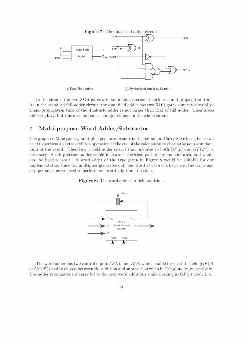
Figure 7: The dual-field adder circuit.c
FSEL
ab
S
Cout
Dual-Field
Adder
a
b
c
FSEL
S
Cout
(a) Dual-Field Adder (b) Synthesized circuit by Mentor
In the circuit, the two XOR gates are dominant in terms of both area and propagation time.As in the standard full-adder circuit, the dual-field adder has two XOR gates connected serially.Thus, propagation time of the dual-field adder is not larger than that of full adder. Their areasdiffer slightly, but this does not cause a major change in the whole circuit.
7 Multi-purpose Word Adder/Subtractor
The proposed Montgomery multiplier generates results in the redundant Carry-Save form, hence weneed to perform an extra addition operation at the end of the calculation to obtain the nonredundantform of the result. Therefore, a field adder circuit that operates in both GF (p) and GF (2m) isnecessary. A full-precision adder would increase the critical path delay and the area, and wouldalso be hard to scale. A word adder of the type given in Figure 8 would be suitable for ourimplementation since the multiplier generates only one word at each clock cycle in the last stageof pipeline, thus we need to perform one word addition at a time.
Figure 8: The word adder for field addition.
Carry
Cin Cout
A
B
CAdder
FSEL A/S
Look-Ahead
clear
The word adder has two control inputs FSEL and A/S , which enable to select the field (GF (p)or GF (2k)) and to choose between the addition and subtraction when in GF (p) mode, respectively.The adder propagates the carry bit to the next word additions while working in GF (p) mode (i.e.,
14

8/7/2019 10.1.1.62.5808
http://slidepdf.com/reader/full/1011625808 15/20
FSEL = 1). Thus, the carry from a word addition operation is delayed using a latch and fed backinto the C in input of the adder for the next word addition at the next clock cycle. In the GF (2m)mode, the module performs only bitwise modulo-2 addition of two input words and the A/S inputis ineffective. An addition operation of two e-word long numbers takes e + 1 clock cycles. The lastcycle generates the carry and prepares the circuit for another operation by zeroing the output of
latch. Figure 9 shows an example of addition operation with operands of 3 words.Figure 9: An example of multiprecision addition operation with e = 3.
A(0)
A(1)
B(0)
B(1)
Word
Adder C (0)
C (1)Word
Adder
0
A
(2)
B(2)
0wC out
C (m-2)Word
Adder
Word
Adder
0w
We added subtraction functionality in the field GF (p) to the word adder because the resultmight be larger than the modulus, and hence one final subtraction operation is necessary as shownin Step 23 of the algorithm in Section 4.1. We do not need this reduction in the GF (2m) case. The
final subtraction operation takes place only if the result is larger than the modulus. Thus, a com-parison operation, which can also be performed utilizing the multi-purpose word adder/subtractor,is required. However, the control circuitry to perform this conditional subtraction might be com-plicated, therefore, it might be placed outside of the Montgomery multiplier unit.
Another reason to include a multi-purpose word adder unit in the multiplier circuit is the factthat the field addition operation is also needed in many cryptographic applications. For example,in elliptic curve cryptosystems, the field addition and multiplication operations are performedsuccessively, hence having the multiplier and adder in the same hardware unit will decrease thecommunication overhead. A word adder that has these properties is synthesized using the MentorGraphics tools and the time and space requirements are obtained, which are given in Table 2.
Table 2: Time and area costs of a multi-purpose word adder for w = 16, 32, 64.
bitsize Propagation Time (ns) Area (in NAND gates)
16 6.87 254
32 9.22 534
64 12.55 1128
Finally, Figure 10 illustrates what happens in last stage of the pipeline. A pair of redundant
words (T C (i)j , T S
(i)j ) are generated each cycle for e clock cycles. The word adder can be used to
15

8/7/2019 10.1.1.62.5808
http://slidepdf.com/reader/full/1011625808 16/20
add these pairs in order to obtain the result words C (i). Note that only one extra cycle is neededto convert the result from the Carry-Save form to the nonredundant form.
Figure 10: Converting the result from the Carry-Save form tothe nonredundant form in the last stage of the pipeline.
a0
B(1)
p(1)
B(2)p(2)
B(0)p(0)
TC(0)
TC(1)
TS(0)
TS(1)
(TC(0),
TS(0))
p(m-1)
0
B(m-1)
0
TC(m-2)
TS(m-2)
TC(m-1)
TS(m-1)C (m-1)
C(m-2)
Word
Adder C (0)
C (1)Word
Adder
Word
Adder
Word
Adder
0
Cout
(TC(1),
TS(1))
(TC(2),
TS(2))
(TC(m-1)
,
TS(m-1)
)
(0w,0w)
8 Design Considerations
In [21], an analysis of the are and time tradeoffs is given for the scalable multiplier. The architectureallows designs with different word lengths and different pipeline organizations for varying valuesof operand precision. In addition, the area can be treated as a design constraint. Thus, one canadjust the design according to the given area, and choose appropriate values for the word lengthand the number of pipeline stages, in accordance. We give a similar analysis for the scalable andunified architecture. We are targeting two different classes of ranges for operand precision:
• High precision range which includes 512, 768 and 1024, is intended for applications requiringthe exponentiation operation.
• Moderate precision range which includes 160, 192, 224, and 256, is typical for elliptic curvecryptography.
The propagation delay of the PU is independent of the wordsize w when w is relatively small, andthus all comparisons among different designs can be made under the assumption that the clock cycleis the same for all cases. The area consumed by the registers for the partial sum, the operands, andmodulus is also the same for all designs, and we are not treating them as parts of the multipliermodule.
The proposed scheme yields the worst performance for the case w = m in the high precisionrange, since some extra cycles are introduced by the PU in order to allow word-serial computation,
16

8/7/2019 10.1.1.62.5808
http://slidepdf.com/reader/full/1011625808 17/20
when compared to other full-precision conventional designs. On the other hand, using many pipelinestages with small wordsize values brings about no advantage after a certain point. Therefore, theperformance evaluation reduces into finding an optimum organization for the circuit.
In order to determine the optimum selection for our organization, we obtain implementationresults by synthesizing the circuit with Mentor Graphics tools using 1.2µm CMOS technology. The
cell area for a given word size w is obtained as
Acell(w) = 48.5w (5)
units, and is slightly different from the one found in [21], where the multiplication factor in theformula is the area cost provided by the synthesis tool for a single bit slice. Note that a 2-inputNAND gate takes up 0.94 units of area. In the pipelined organization, the area of the inter-stagelatches is important, which was measured as
Alatch(w) = 8.32w (6)
units. Thus, the area of a pipeline with k processing elements is given as
Apipe(k, w) = (k − 1)Alatch(w) + kAcell(w) = 56, 82kw − 8.32w (7)
units. For a given area, we are able to evaluate different organizations and select the most suitableone for our application. The graphs given in Figure 11 allow to make such evaluations for a fixedarea of 15,000 gates.
Figure 11: Time efficiency for different configurationswith a fixed area of 15,000 gates.
0 10 20 30300
350
400
450
500
550
600
Number of Stages
Time (Clock Cycles)
Time for Moderate Precision
m=160
m=192
m=224
m=256
0 10 20 301000
1500
2000
2500
3000
3500
4000
4500
5000
5500
Number of Stages
Time for High Precision
Time(Clock Cycles)
m=512
m=768
m=1024
For both moderate and high precision ranges, the number of stages between 5 and 10 arelikely to give the best performance. For the high precision cases, fewer than 5 stages yields very
17
8/7/2019 10.1.1.62.5808
http://slidepdf.com/reader/full/1011625808 18/20
poor performance since the fixed area becomes insufficient for large wordsizes and the performancedegradation due to pipeline stalls becomes a major problem. The small number of stages with verylong word sizes seem to provide a reasonable performance in the moderate range, however, becauseof the incompatibility issues about using very long word sizes and inefficiency when the precisionincreases, using fewer than 5 stages is not advised. We avoid using many stages for two reasons:
• high utilization of the PUs will be possible only for very high precision, and
• the execution time may have undesirable oscillations.
The behavior mentioned in the latter category is the result of the facts that
• extra stages at the end of the computations, and
• there is not a good match between the number of words e and the number of stages k, causinga underutilization of stages in the pipeline.
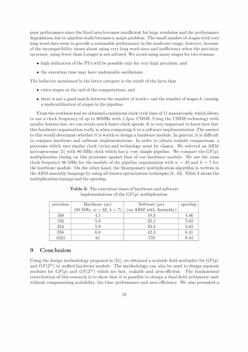
From the synthesis tool we obtained a minimum clock cycle time of 11 nanoseconds, which allowsto use a clock frequency of up to 90MHz with 1.2µm CMOS. Using the CMOS technology with
smaller feature size, we can attain much faster clock speeds. It is very important to know how fastthis hardware organization really is when comparing it to a software implementation. The answerto this would determine whether it is worth to design a hardware module. In general, it is difficultto compare hardware and software implementations. In order to obtain realistic comparisons, aprocessor which uses similar clock cycles and technology must be chosen. We selected an ARMmicroprocessor [5] with 80 MHz clock which has a very simple pipeline. We compare the GF (p)multiplication timing on this processor against that of our hardware module. We use the sameclock frequency 80 MHz for the module of the pipeline organization with w = 32 and k = 7 forthe hardware module. On the other hand, the Montgomery multiplication algorithm is written inthe ARM assembly language by using all known optimization techniques [8, 10]. Table 3 shows themultiplication timings and the speedup.
Table 3: The execution times of hardware and softwareimplementations of the GF (p) multiplication.
precision Hardware (µs) Software (µs) speedup(80 MHz, w = 32, k = 7) (on ARM with Assembly)
160 4.1 18.3 4.46
192 5.0 25.1 5.02
224 5.9 33.2 5.63
256 6.6 42.3 6.41
1024 61 570 9.34
9 Conclusion
Using the design methodology proposed in [21], we obtained a scalable field multiplier for GF (p)and GF (2m) in unified hardware module. The methodology can also be used to design separatemodules for GF (p) and GF (2m) which are fast, scalable and area-efficient. The fundamentalcontribution of this research is to show that it is possible to design a dual-field arithmetic unitwithout compromising scalability, the time performance and area efficiency. We also presented a
18

8/7/2019 10.1.1.62.5808
http://slidepdf.com/reader/full/1011625808 19/20
dual-field addition module which is suitable for the pipeline organization of the multiplier. Theadder is scalable and capable of performing addition in both types of fields. Our analysis shows thata pipeline consisting of several stages is adequate and more efficient than a single unit processingvery long words. Working with relatively short words diminishes data paths in the final circuit,reducing the required bandwidth.
The proposed multiplier was synthesized using the Mentor tools, and a circuit capable of workingwith clock frequencies up to 90 MHz is obtained. Except for the upper limit on the precision whichis dictated only by the availability of memory to store the operands and internal results, the moduleis capable of performing infinite-precision Montgomery multiplication in GF (2m) and GF (p).
References
[1] G. B. Agnew, R. C. Mullin, and S. A. Vanstone. An implementation of elliptic curve cryp-tosystems over F 2155 . IEEE Journal on Selected Areas in Communications, 11(5):804–813,June 1993.
[2] A. Bernal and A. Guyot. Design of a modular multiplier based on Montgomery’s algorithm. In13th Conference on Design of Circuits and Integrated Systems, pages 680–685, Madrid, Spain,November 17–20 1998.
[3] W. Diffie and M. E. Hellman. New directions in cryptography. IEEE Transactions on Infor-
mation Theory , 22:644–654, November 1976.
[4] S. E. Eldridge and C. D. Walter. Hardware implementation of Montgomery’s modular multi-plication algorithm. IEEE Transactions on Computers, 42(6):693–699, June 1993.
[5] Steve Furber. ARM System Architecture. Addison-Wesley, Reading, MA, 1997.
[6] B. S. Kaliski Jr. The Montgomery inverse and its applications. IEEE Transactions on Com-
puters, 44(8):1064–1065, August 1995.
[7] N. Koblitz. Elliptic curve cryptosystems. Mathematics of Computation , 48(177):203–209,January 1987.
[8] C. K. Koc. High-Speed RSA Implementation. Technical Report TR 201, RSA Laboratories,73 pages, November 1994.
[9] C. K. Koc and T. Acar. Montgomery multiplication in GF(2k). Designs, Codes and Cryptog-
raphy , 14(1):57–69, April 1998.
[10] C. K. Koc, T. Acar, and B. S. Kaliski Jr. Analyzing and comparing Montgomery multiplicationalgorithms. IEEE Micro, 16(3):26–33, June 1996.
[11] P. Kornerup. High-radix modular multiplication for cryptosystems. In E. Swartzlander, Jr.,M. J. Irwin, and G. Jullien, editors, Proceedings, 11th Symposium on Computer Arithmetic,pages 277–283, Windsor, Ontario, June 29 – July 2 1993. IEEE Computer Society Press, LosAlamitos, CA.
[12] A. J. Menezes. Elliptic Curve Public Key Cryptosystems. Kluwer Academic Publishers, Boston,MA, 1993.
19

8/7/2019 10.1.1.62.5808
http://slidepdf.com/reader/full/1011625808 20/20
[13] P. L. Montgomery. Modular multiplication without trial division. Mathematics of Computation ,44(170):519–521, April 1985.
[14] D. Naccache and D. M’Raıhi. Cryptographic smart cards. IEEE Micro, 16(3):14–24, June1996.
[15] National Institute for Standards and Technology. Digital Signature Standard (DSS). FIPSPUB 186-2, January 2000.
[16] J.-H. Oh and S.-J. Moon. Modular multiplication method. IEE Proceedings: Computers and
Digital Techniques, 145(4):317–318, July 1998.
[17] H. Orup. Simplifying quotient determination in high-radix modular multiplication. InS. Knowles and W. H. McAllister, editors, Proceedings, 12th Symposium on Computer Arith-
metic, pages 193–199, Bath, England, July 19–21 1995. IEEE Computer Society Press, LosAlamitos, CA.
[18] J.-J. Quisquater and C. Couvreur. Fast decipherment algorithm for RSA public-key cryptosys-
tem. Electronics Letters, 18(21):905–907, October 1982.[19] A. Royo, J. Moran, and J. C. Lopez. Design and implementation of a coprocessor for cryptog-
raphy applications. In European Design and Test Conference, pages 213–217, Paris, France,March 17-20 1997.
[20] E. Savas and C. K. Koc. The Montgomery modular inverse - revisited. IEEE Transactions on
Computers, to appear, 2000.
[21] A. F. Tenca and C. K. Koc. A scalable architecture for Montgomery multiplication. In C.K. Koc and C. Paar, editors, Cryptographic Hardware and Embedded Systems, Lecture Notesin Computer Science, No. 1717, pages 94–108. Springer, Berlin, Germany, 1999.
[22] C. D. Walter. Space/Time trade-offs for higher radix modular multiplication using repeatedaddition. IEEE Transactions on Computers, 46(2):139–141, February 1997.
20