ud info corp. - applikationsspezialist für elektronische ... · ud info corp. industrial m.2 22110...
TRANSCRIPT
Product Datasheet
UD info Corp. Industrial M.2 22110 PCIe SSD
M2P-10UD Series Product DataSheet
UD info CORP. 3F-4, No.8, Ln. 609, Sec. 5, Chongxin Rd., Sanchong Dist., New Taipei City 241, Taiwan (R.O.C.)
TEL: +886-2-7713-6050 FAX: +886-2-8511-3151 E-mail: [email protected]

Product Datasheet
UD info CORP. TEL: +886-2-7713-6050 FAX: +886-2-8511-3151 3F-4, No.8, Ln. 609, Sec. 5, Chongxin Rd., Sanchong Dist., New Taipei City 241, Taiwan (R.O.C.)
2
1. Introduction ................................................................................................ 51.1. General Description ......................................................................................................... 5
1.2. Block Diagram ................................................................................................................. 5
2. Product Specifications ................................................................................. 6
3. Environmental Specifications ..................................................................... 83.1. Environmental Conditions ............................................................................................... 8
3.1.1. Temperature and Humidity .................................................................................. 83.1.2. Shock .................................................................................................................... 93.1.3. Vibration ............................................................................................................... 93.1.4. Drop ..................................................................................................................... 93.1.5. Bending ................................................................................................................ 93.1.6. Torque .................................................................................................................. 93.1.7. Electrostatic Discharge (ESD) ........................................................................... 10
3.2. MTBF ............................................................................................................................. 10
3.3. Certification ................................................................................................................... 10
3.4. Compliance .................................................................................................................... 10
4. Electrical Specifications ............................................................................ 114.1. Supply Voltage ............................................................................................................... 11
4.2. Power Consumption ....................................................................................................... 11
5. Interface .................................................................................................... 125.1. Pin Assignment and Descriptions .................................................................................. 12
6. Supported Commands ............................................................................... 156.1. NVMe Command List .................................................................................................... 15
6.2. Identify Device Data ...................................................................................................... 16
7. Physical Dimension ................................................................................... 20
8. Terminology .............................................................................................. 22
9. Barcode description .................................................................................. 22
10. Partnumber decoder ................................................................................. 23

Product Datasheet
UD info CORP. TEL: +886-2-7713-6050 FAX: +886-2-8511-3151 3F-4, No.8, Ln. 609, Sec. 5, Chongxin Rd., Sanchong Dist., New Taipei City 241, Taiwan (R.O.C.)
3
Revision History Revision Draft Date History Author
1.0 2016/5/6 New release Golden Lee
1.1 2016/7/1 Modify P/N decoder code X14 to “E” Golden Lee
1.2 2016/7/20 Update support capacity and Low power Golden Lee
1.3 2016/8/12 Update performance Golden Lee

Product Datasheet
UD info CORP. TEL: +886-2-7713-6050 FAX: +886-2-8511-3151 3F-4, No.8, Ln. 609, Sec. 5, Chongxin Rd., Sanchong Dist., New Taipei City 241, Taiwan (R.O.C.)
4
Product Overview
Capacity ■ MLC: 240GB (256GB) up to 960GB (1TB)
Form Factor ■ M.2 22110-D5-M
PCIe Interface ■ PCIe Gen3 x4
Compliance ■ NVMe 1.2 ■ PCI Express Base 3.0
Flash Interface ■ Flash Type: MLC ■ Up to 8pcs of BGA flash
Performance ■ Read up to 2,800 MB/s ■ Write up to 1,550 MB/s
Power ConsumptionNote1 ■ Active mode: <7300mW
TBW (Terabyte Written) ■ MLC: 1396 TBW for 960GB
MTBF ■ MLC: 2,000,000 hours
Advanced Flash Management ■ Static and Dynamic Wear Leveling ■ Bad Block Management ■ TRIM ■ SMART ■ Over-Provision
Power Saving Modes ■ Support APST ■ Support ASPM ■ Support L1.2
Temperature Range ■ Operation (Standard): 0°C ~ 65°C ■ Storage: -40°C ~ 85°C
Compliant ■ RoHS ■ CE & FCC (TBD)
Notes: 1. Please see “Power Consumption” for details.

Product Datasheet
UD info CORP. TEL: +886-2-7713-6050 FAX: +886-2-8511-3151 3F-4, No.8, Ln. 609, Sec. 5, Chongxin Rd., Sanchong Dist., New Taipei City 241, Taiwan (R.O.C.)
5
1. INTRODUCTION 1.1. General Description UDinfo’s M.2 22110 PCIe solid state Drive delivers all the advantages of flash disk technology with PCIe
Gen3 x4 interface and is fully compliant with the standard Next Generation Form Factor (NGFF) called M.2
Card Format, which is generated by Intel. The M.2 22110 could provide a wide range capacity up to 960GB
and reach up to 2,800MB/s read as well as 1,550MB/s write high performance based on Toshiba’s 15nm
Toggle MLC flash (with 256MB/512MB/1024MB DDR3L cache enabled and measured by CrystalDiskMark
v5.0). Moreover, the power consumption of the M.2 22110 is much lower than traditional hard drives,
making it the best embedded solution for new platforms
1.2. Block Diagram
M.2 22110 PCIe SSD Block Diagram
Flash Controller
DDR3L Data Buffer
Data Flash Array
DC-DC Flash memory
PCIe Interface
VCC
Vcore
A+
A-
B+
B- Control signal
VCC
PCIe PHY Gen3 x4 NVMe 1.2

Product Datasheet
UD info CORP. TEL: +886-2-7713-6050 FAX: +886-2-8511-3151 3F-4, No.8, Ln. 609, Sec. 5, Chongxin Rd., Sanchong Dist., New Taipei City 241, Taiwan (R.O.C.)
6
2. PRODUCT SPECIFICATIONS Capacity
■ MLC: From 240GB (256GB) up to 960GB (1TB) (support 48-bit addressing mode)
Electrical/Physical Interface
■ PCIe Interface
Compliant with NVMe 1.2
Compatible with PCIe I/II/III x 4 interface
Support up to queue depth 64K
Support power management
Supported NAND Flash
■ Toshiba 15nm MLC, TLC, Toggle1.0 and Toggle2.0
■ Support all types of MLC/TLC large block: 8KB/page and 16K/page NAND flash
■ Contain up to 8pcs of BGA flash
ECC Scheme
■ Up to 120 bits / 2K Byte
UART function
GPIO
Support SMART and TRIM commands

Product Datasheet
UD info CORP. TEL: +886-2-7713-6050 FAX: +886-2-8511-3151 3F-4, No.8, Ln. 609, Sec. 5, Chongxin Rd., Sanchong Dist., New Taipei City 241, Taiwan (R.O.C.)
7
Performance
■ MLC:
Capacity Flash
Structure Flash Type
Sequential
Read
(MB/s)
Write
(MB/s)
240GB (256GB) 32GB x 8 15nm, BGA (4-Plane) 2,750 1,500
480GB (512GB) 64GB x 8 15nm, BGA (4-Plane) 2,800 1,550
960GB (1TB) 128GB x 8 15nm, BGA (4-Plane) 2,800 1,550
Notes:
1. The performance was estimated based on Toshiba MLC NAND flash.
2. Performance may differ according to flash configuration and platform.
3. The table above is for reference only. The criteria for MP (mass production) and for accepting
goods shall be discussed based on different flash configuration.
TBW (Terabytes Written)
■ MLC:
Capacity Flash Structure TBW
240GB (256GB) 32GB x 8 349
480GB (512GB) 64GB x 8 698
960GB (1TB) 128GB x 8 1,396
Notes:
1. Samples were built using Toshiba MLC NAND flash.
2. TBW may differ according to flash configuration and platform.
3. The endurance of SSD could be estimated based on user behavior, NAND endurance cycles, and
write amplification factor. It is not guaranteed by flash vendor.

Product Datasheet
UD info CORP. TEL: +886-2-7713-6050 FAX: +886-2-8511-3151 3F-4, No.8, Ln. 609, Sec. 5, Chongxin Rd., Sanchong Dist., New Taipei City 241, Taiwan (R.O.C.)
8
3. ENVIRONMENTAL SPECIFICATIONS 3.1. Environmental Conditions 3.1.1. Temperature and Humidity
Temperature:
Storage: -40°C to 85°C
Operational (Standard grade): 0°C to 65°C
Humidity:
Standard grade: RH 90% under 40°C (operational)
High Temperature Test Condition
Temperature Humidity Test Time
Operation (Standard)
Operation (Wide)
65°C
85°C
0% RH
0% RH
72 hours
72 hours
Result: No any abnormality is detected.
Low Temperature Test Condition
Temperature Humidity Test Time
Operation (Standard) 0°C 0% RH 72 hours
Storage (Standard) -40°C 0% RH 72 hours
Result: No any abnormality is detected.
High Humidity Test Condition
Temperature Humidity Test Time
Operation (Standard) 40°C 90% RH 4 hours
Storage (Standard) 40°C 93% RH 72 hours
Result: No any abnormality is detected.
Temperature Cycle Test
Temperature Test Time Cycle
Operation (Standard) 0°C 30 min
10 cycles 65°C 30 min
Storage (Standard) -40°C 30 min
10 cycles 85°C 30 min
Result: No any abnormality is detected.

Product Datasheet
UD info CORP. TEL: +886-2-7713-6050 FAX: +886-2-8511-3151 3F-4, No.8, Ln. 609, Sec. 5, Chongxin Rd., Sanchong Dist., New Taipei City 241, Taiwan (R.O.C.)
9
3.1.2. Shock Shock Specification
Acceleration Force Half Sin Pulse Duration
Non-Operational 1500G 0.5ms
Result: No any abnormality is detected.
3.1.3. Vibration Vibration Specification
Condition Vibration Orientation
Frequency/Displacement Frequency/Acceleration
Non-Operational 20Hz~80Hz/1.52mm 80Hz~2000Hz/20G X, Y, Z axis/60 min for each
Result: No any abnormality is detected.
3.1.4. Drop Drop Specification
Height of Drop Number of Drop
Non-operational 80cm free fall 6 face of each unit
Result: No any abnormality is detected.
3.1.5. Bending Bending Specification
Force Action
Non-operational ≥ 20N Hold 1min/5times
Result: No any abnormality is detected.
3.1.6. Torque Contact ESD Specification
Force Action
Non-operational 0.5N-m or ±2.5 deg Hold 1min/5times
Result: No any abnormality is detected.
Product Datasheet
UD info CORP. TEL: +886-2-7713-6050 FAX: +886-2-8511-3151 3F-4, No.8, Ln. 609, Sec. 5, Chongxin Rd., Sanchong Dist., New Taipei City 241, Taiwan (R.O.C.)
10
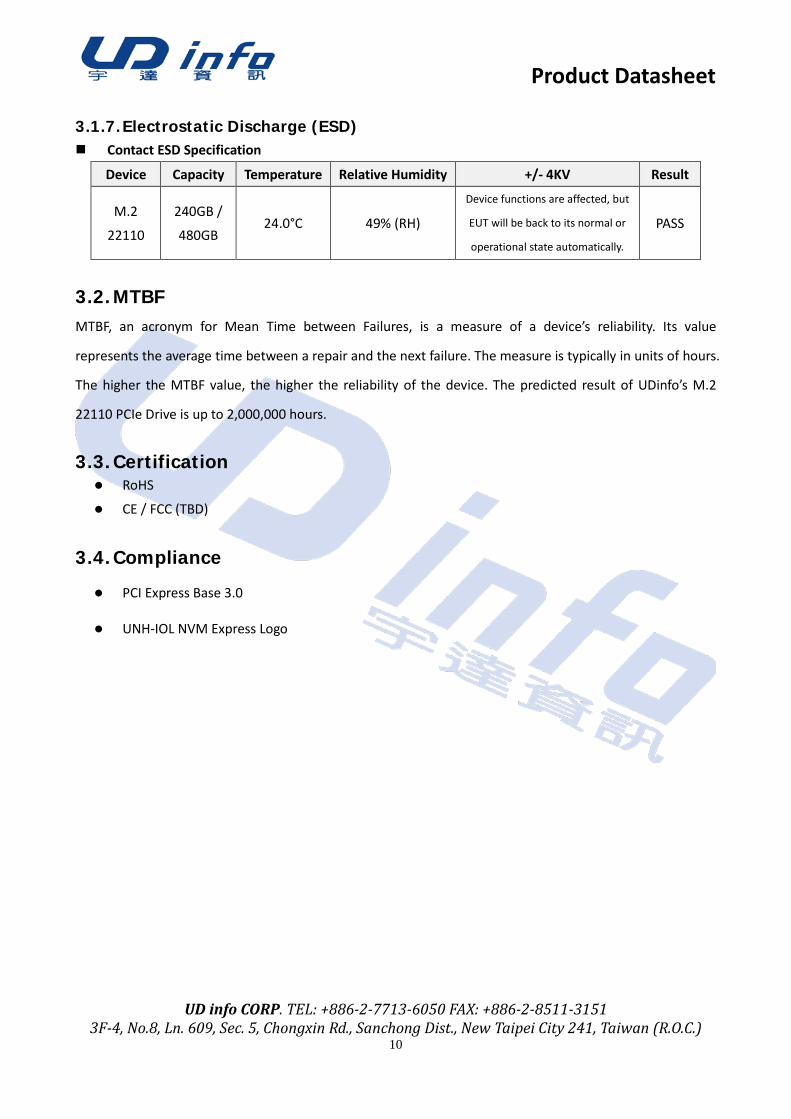
3.1.7. Electrostatic Discharge (ESD) Contact ESD Specification
Device Capacity Temperature Relative Humidity +/- 4KV Result
M.2
22110
240GB /
480GB 24.0°C 49% (RH)
Device functions are affected, but
EUT will be back to its normal or
operational state automatically.
PASS
3.2. MTBF MTBF, an acronym for Mean Time between Failures, is a measure of a device’s reliability. Its value
represents the average time between a repair and the next failure. The measure is typically in units of hours.
The higher the MTBF value, the higher the reliability of the device. The predicted result of UDinfo’s M.2
22110 PCIe Drive is up to 2,000,000 hours.
3.3. Certification RoHS
CE / FCC (TBD)
3.4. Compliance PCI Express Base 3.0
UNH-IOL NVM Express Logo

Product Datasheet
UD info CORP. TEL: +886-2-7713-6050 FAX: +886-2-8511-3151 3F-4, No.8, Ln. 609, Sec. 5, Chongxin Rd., Sanchong Dist., New Taipei City 241, Taiwan (R.O.C.)
11
4. ELECTRICAL SPECIFICATIONS 4.1. Supply Voltage
Parameter Rating
Operating Voltage 3.3V
4.2. Power Consumption
■ MLC Capacity Flash Structure Flash Type Read Write Idle L1.2
240GB (256GB) 32GB x 8 15nm, BGA 5,200 4,950 400 5
480GB (512GB) 64GB x 8 15nm, BGA 5,500 7,050 400 5
960GB (1TB) 128GB x 8 15nm, BGA 6,000 7,300 400 5
Unit: mW
NOTES:
1. The average value of power consumption is achieved based on 100% conversion efficiency.
2. The measured power voltage is 3.3V.
3. Samples were built using Toshiba NAND flash and measured under normal temperature.
4. Sequential R/W is measured while testing 4000MB sequential R/W 5 times by CyrstalDiskMark.
5. Power Consumption may differ according to flash configuration and platform.

Product Datasheet
UD info CORP. TEL: +886-2-7713-6050 FAX: +886-2-8511-3151 3F-4, No.8, Ln. 609, Sec. 5, Chongxin Rd., Sanchong Dist., New Taipei City 241, Taiwan (R.O.C.)
12
5. INTERFACE 5.1. Pin Assignment and Descriptions The follow table defines the signal assignment of the internal NGFF connector for SSD usage, described in
the PCI Express M.2 Specification version 1.0 of the PCI-SIG.
Pin # SATA Pin Description
1 GND Ground
2 3.3V 3.3V source
3 GND Ground
4 3.3V 3.3V source
5 PETn3 PCIe TX Differential signal defined by the PCI Express M.2 spec
6 N/C No connect
7 PETp3 PCIe TX Differential signal defined by the PCI Express M.2 spec
8 N/C No connect
9 GND Ground
10 LED1#(O) Status indicators via LED devices
11 PERn3 PCIe RX Differential signal defined by the PCI Express M.2 spec
12 3.3V 3.3V source
13 PERp3 PCIe RX Differential signals defined by the PCI Express M.2 spec.
14 3.3V 3.3V source
15 GND Ground
16 3.3V 3.3V source
17 PETn2 PCIe TX Differential signal defined by the PCI Express M.2 spec
18 3.3V 3.3V source
19 PETp2 PCIe TX Differential signal defined by the PCI Express M.2 spec
20 N/C No connect
21 GND Ground
22 N/C No connect
23 PERn2 PCIe RX Differential signal defined by the PCI Express M.2 spec
24 N/C No connect
25 PERp2 PCIe RX Differential signal defined by the PCI Express M.2 spec
26 N/C No connect
27 GND Ground
28 N/C No connect
29 PETn1 PCIe TX Differential signal defined by the PCI Express M.2 spec
30 N/C No connect

Product Datasheet
UD info CORP. TEL: +886-2-7713-6050 FAX: +886-2-8511-3151 3F-4, No.8, Ln. 609, Sec. 5, Chongxin Rd., Sanchong Dist., New Taipei City 241, Taiwan (R.O.C.)
13
Pin # SATA Pin Description
31 PETp1 PCIe TX Differential signal defined by the PCI Express M.2 spec
32 N/C No connect
33 GND Ground
34 N/C No connect
35 PERn1 PCIe RX Differential signal defined by the PCI Express M.2 spec
36 N/C No connect
37 PERp1 PCIe RX Differential signal defined by the PCI Express M.2 spec
38 N/C No connect
39 GND Ground
40 N/C No connect
41 PETn0 PCIe TX Differential signal defined by the PCI Express M.2 spec
42 N/C No connect
43 PETp0 PCIe TX Differential signal defined by the PCI Express M.2 spec
44 N/C No connect
45 GND Ground
46 N/C No connect
47 PERn0 PCIe RX Differential signal defined by the PCI Express M.2 spec
48 N/C No connect
49 PERp0 PCIe RX Differential signal defined by the PCI Express M.2 spec
50 PERST#(I)(0/3.3V) PE-Reset is a functional reset to the card as defined by the PCIe Mini CEM
specification.
51 GND Ground
52 CLKREQ#(I/O)(0/3.3V) Clock Request is a reference clock request signal as defined by the PCIe
Mini CEM specification; Also used by L1 PM Substates.
53 REFCLKn PCIe Reference Clock signals (100 MHz) defined by the PCI Express M.2
spec.
54 PEWAKE#(I/O)(0/3.3V) PCIe PME Wake.
Open Drain with pull up on platform; Active Low.
55 REFCLKp PCIe Reference Clock signals (100 MHz) defined by the PCI Express M.2
spec.
56 Reserved for
MFG DATA
Manufacturing Data line. Used for SSD manufacturing only.
Not used in normal operation.
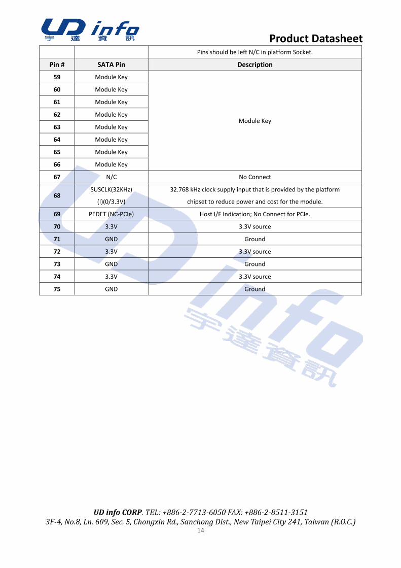
Pins should be left N/C in platform Socket.
57 GND Ground
58 Reserved for MFG
CLOCK
Manufacturing Clock line. Used for SSD manufacturing only.
Not used in normal operation.
Product Datasheet
UD info CORP. TEL: +886-2-7713-6050 FAX: +886-2-8511-3151 3F-4, No.8, Ln. 609, Sec. 5, Chongxin Rd., Sanchong Dist., New Taipei City 241, Taiwan (R.O.C.)
14
Pins should be left N/C in platform Socket.
Pin # SATA Pin Description
59 Module Key
Module Key
60 Module Key
61 Module Key
62 Module Key
63 Module Key
64 Module Key
65 Module Key
66 Module Key
67 N/C No Connect
68 SUSCLK(32KHz)
(I)(0/3.3V)
32.768 kHz clock supply input that is provided by the platform
chipset to reduce power and cost for the module.
69 PEDET (NC-PCIe) Host I/F Indication; No Connect for PCIe.
70 3.3V 3.3V source
71 GND Ground
72 3.3V 3.3V source
73 GND Ground
74 3.3V 3.3V source
75 GND Ground

Product Datasheet
UD info CORP. TEL: +886-2-7713-6050 FAX: +886-2-8511-3151 3F-4, No.8, Ln. 609, Sec. 5, Chongxin Rd., Sanchong Dist., New Taipei City 241, Taiwan (R.O.C.)
15
6. SUPPORTED COMMANDS
6.1. NVMe Command List
Table 6-1 Admin Commands
Op-Code Command Description
00h Delete I/O Submission Queue
01h Create I/O Submission Queue
02h Get Log Page
04h Delete I/O Completion Queue
05h Create I/O Completion Queue
06h Identify
08h Abort
09h Set Features
0Ah Get Features
0Ch Asynchronous Event Request
10h Firmware Activate
11h Firmware Image Download
Table 6-2 Admin Commands – NVM Command Set Specific
Op-Code Command Description
80h Format NVM
81h Security Send
82h Security Receive
Table 6-3 NVM Commands
Op-Code Command Description
00h Flush
01h Write
02h Read
04h Write Uncorrectable
05h Compare
08h Write Zeroes
09h Dataset Management

Product Datasheet
UD info CORP. TEL: +886-2-7713-6050 FAX: +886-2-8511-3151 3F-4, No.8, Ln. 609, Sec. 5, Chongxin Rd., Sanchong Dist., New Taipei City 241, Taiwan (R.O.C.)
16
6.2. Identify Device Data The following table details the sector data returned by the IDENTIFY DEVICE command.
Identify Controller Data Structure Bytes Description
Controller Capabilities and Features
01:00 PCI Vendor ID (VID)
03:02 PCI Subsystem Vendor ID (SSVID)
23:04 Serial Number (SN)
63:24 Model Number (MN)
71:64 Firmware Revision (FR)
72 Recommended Arbitration Burst (RAB)
75:73 IEEE OUI Identifier (IEEE)
76 Controller Multi-Path I/O and Namespace Sharing Capabilities (CMIC)
77 Maximum Data Transfer Size (MDTS)
255:80 Reserved
Admin Command Set Attributes & Optional Controller Capabilities
257:256 Optional Admin Command Support (OACS)
258 Abort Command Limit (ACL)
259 Asynchronous Event Request Limit (AERL)
260 Firmware Updates (FRMW)
261 Log Page Attributes (LPA)
262 Error Log Page Entries (ELPE)
263 Number of Power States Support (NPSS)
264 Admin Vendor Specific Command Configuration (AVSCC)
265 Autonomous Power State Transition Attributes (APSTA)
511:266 Reserved
NVM Command Set Attributes
512 Submission Queue Entry Size (SQES)
513 Completion Queue Entry Size (CQES)
515:514 Reserved
519:516 Number of Namespaces (NN)
521:520 Optional NVM Command Support (ONCS)
523:522 Fused Operation Support (FUSES)
524 Format NVM Attributes (FNA)
525 Volatile Write Cache (VWC)

Product Datasheet
UD info CORP. TEL: +886-2-7713-6050 FAX: +886-2-8511-3151 3F-4, No.8, Ln. 609, Sec. 5, Chongxin Rd., Sanchong Dist., New Taipei City 241, Taiwan (R.O.C.)
17
Bytes Description
527:526 Atomic Write Unit Normal (AWUN)
529:528 Atomic Write Unit Power Fail (AWUPF)
530 NVM Vendor Specific Command Configuration (NVSCC)
531 Reserved
533:532 Atomic Compare & Write Unit (ACWU)
535:534 Reserved
539:536 SGL Support (SGLS)
703:540 Reserved

Product Datasheet
UD info CORP. TEL: +886-2-7713-6050 FAX: +886-2-8511-3151 3F-4, No.8, Ln. 609, Sec. 5, Chongxin Rd., Sanchong Dist., New Taipei City 241, Taiwan (R.O.C.)
18
Identify Namespace Data Structure & NVM Command Set Specific Bytes Description
7:0 Namespace Size (NSZE)
15:8 Namespace Capacity (NCAP)
23:16 Namespace Utilization (NUSE)
24 Namespace Features (NSFEAT)
25 Number of LBA Formats (NLBAF)
26 Formatted LBA Size (FLBAS)
27 Metadata Capabilities (MC)
28 End-to-end Data Protection Capabilities (DPC)
29 End-to-end Data Protection Type Settings (DPS)
30 Namespace Multi-path I/O and Namespace Sharing Capabilities (NMIC)
31 Reservation Capabilities (RESCAP)
119:32 Reserved
127:120 IEEE Extended Unique Identifier (EUI64)
131:128 LBA Format 0 Support (LBAF0)
135:132 LBA Format 1 Support (LBAF1)
139:136 LBA Format 2 Support (LBAF2)
143:140 LBA Format 3 Support (LBAF3)
147:144 LBA Format 4 Support (LBAF4)
151:148 LBA Format 5 Support (LBAF5)
155:152 LBA Format 6 Support (LBAF6)
159:156 LBA Format 7 Support (LBAF7)
163:160 LBA Format 8 Support (LBAF8)
167:164 LBA Format 9 Support (LBAF9)
171:168 LBA Format 10 Support (LBAF10)
175:172 LBA Format 11 Support (LBAF11)
179:176 LBA Format 12 Support (LBAF12)
183:180 LBA Format 13 Support (LBAF13)
187:184 LBA Format 14 Support (LBAF14)
191:188 LBA Format 15 Support (LBAF15)
383:192 Reserved
4095:384 Vendor Specific (VS)

Product Datasheet
UD info CORP. TEL: +886-2-7713-6050 FAX: +886-2-8511-3151 3F-4, No.8, Ln. 609, Sec. 5, Chongxin Rd., Sanchong Dist., New Taipei City 241, Taiwan (R.O.C.)
19
List of Identify Namespace Data Structure for Each Capacity Capacity
(GB)
Byte[7:0]:
Namespace Size (NSZE)
240 1BF244B0h
256 1DCF32B0h
480 37E436B0h
512 3B9E12B0h
960 6FC81AB0h
1024 773BD2B0h

Product Datasheet
UD info CORP. TEL: +886-2-7713-6050 FAX: +886-2-8511-3151 3F-4, No.8, Ln. 609, Sec. 5, Chongxin Rd., Sanchong Dist., New Taipei City 241, Taiwan (R.O.C.)
20
7. PHYSICAL DIMENSION Dimension: 110mm(L) x 22mm(W) x 3.80mm(H)
Top View
Bottom View

Product Datasheet
UD info CORP. TEL: +886-2-7713-6050 FAX: +886-2-8511-3151 3F-4, No.8, Ln. 609, Sec. 5, Chongxin Rd., Sanchong Dist., New Taipei City 241, Taiwan (R.O.C.)
21
Side View
*Notes:
1. =Max Component Height
2. =No Component
3. =No Component / Signal Vias / Signal Copper / Print
4. General Tolerance: ±0.15mm
5. Check Point: ①~③

Product Datasheet
UD info CORP. TEL: +886-2-7713-6050 FAX: +886-2-8511-3151 3F-4, No.8, Ln. 609, Sec. 5, Chongxin Rd., Sanchong Dist., New Taipei City 241, Taiwan (R.O.C.)
22
8. TERMINOLOGY
The following table is to list out the acronyms that have been applied throughout the document.
Term Definitions
ATTO Commercial performance benchmark application
DDR Double data rate (SDRAM)
DIPM Device initiated power management
HIPM Host initiated power management
LBA Logical block addressing
MB Mega-byte
MTBF Mean time between failures
PCIe PCI Express / Peripheral Component Interconnect Express
S.M.A.R.T. Self-monitoring, analysis and reporting technology
SSD Solid state disk
9. BARCODE DESCRIPTION
M 2 P 1 0 U D 9 6 0 G B K E P
yymmddXX
Part Number
Manufacturing
Data: YYMMDD Flash Type:

Product Datasheet
UD info CORP. TEL: +886-2-7713-6050 FAX: +886-2-8511-3151 3F-4, No.8, Ln. 609, Sec. 5, Chongxin Rd., Sanchong Dist., New Taipei City 241, Taiwan (R.O.C.)
23
10. PARTNUMBER DECODER
M2P-10UDX8X9X10X11X12X13X14X15X16X17
X1X2X3 X4X5 X6X7 X8 X9 X10 X11 X12 X13 X14 X15 X16X17
M2P 10 UD
240GB
480GB
960GB
256GB
512GB
001TB
K: MLC Standard (0ºC ~ +70ºC) E P blank