mxtwxyttda
TRANSCRIPT
7252019 mXtwxytTDA
httpslidepdfcomreaderfullmxtwxyttda 117
TEA7532
July 1993
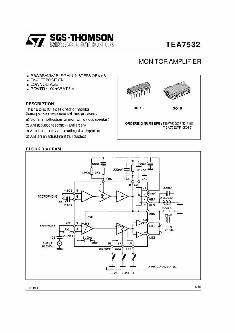
MONITOR AMPLIFIER
PROGRAMMABLE GAIN IN STEPS OF 6 dBONOFF POSITION LOW VOLTAGEPOWER 100 mW AT 5 V
DESCRIPTION
This 16 pins IC is designed for monitor(loudspeaker)telephone set and provides
a) Signal amplification for monitoring (loudspeaker)
b) Antiacoustic feedback (antilarsen)
c) Antidistortion by automatic gain adaptation
d) Antilarsen adjustment (full duplex)
DIP16 SO16
ORDERING NUMBERS TEA7532DP (DIP16)TEA7532FP (SO16)
BLOCK DIAGRAM
116
7252019 mXtwxytTDA
httpslidepdfcomreaderfullmxtwxyttda 217
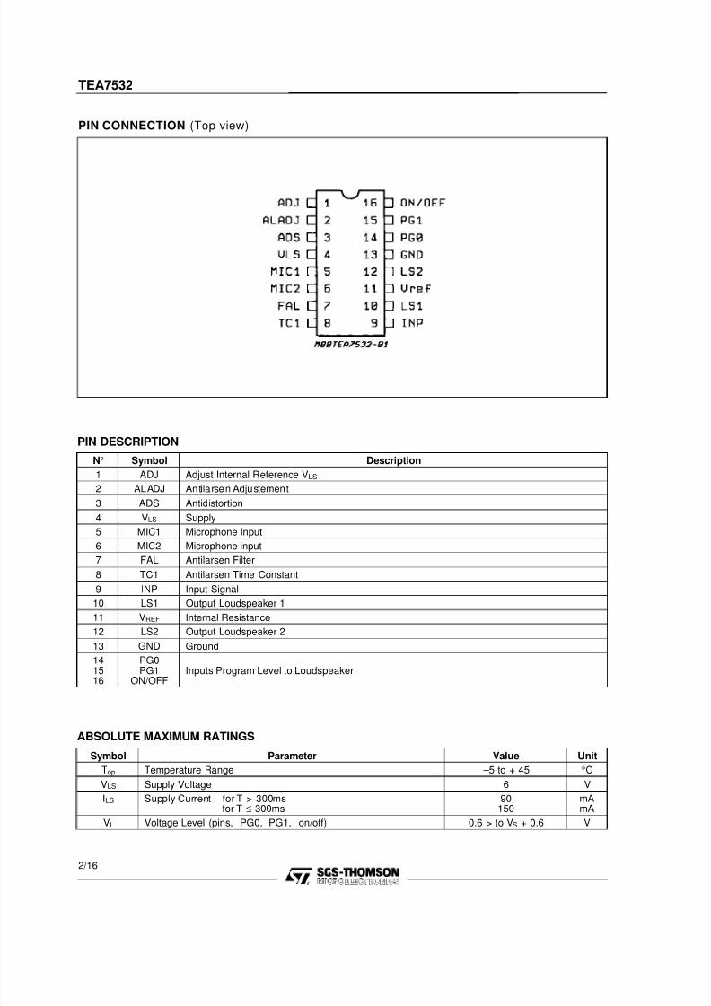
PIN DESCRIPTION
Ndeg Symbol Description
1 ADJ Adjust Internal Reference VLS
2 ALADJ Antilarsen Adjustement
3 ADS Antidistortion
4 VLS Supply
5 MIC1 Microphone Input
6 MIC2 Microphone input
7 FAL Antilarsen Filter
8 TC1 Antilarsen Time Constant
9 INP Input Signal
10 LS1 Output Loudspeaker 1
11 VREF Internal Resistance
12 LS2 Output Loudspeaker 2
13 GND Ground
141516
PG0PG1
ONOFFInputs Program Level to Loudspeaker
PIN CONNECTION (Top view)
ABSOLUTE MAXIMUM RATINGS
Symbol Parameter Value Unit
Top Temperature Range ndash5 to + 45 degC
VLS Supply Voltage 6 V
ILS Supply Current for T gt 300msfor T le 300ms
90150
mAmA
VL Voltage Level (pins PG0 PG1 onoff) 06 gt to VS + 06 V
TEA7532
216
7252019 mXtwxytTDA
httpslidepdfcomreaderfullmxtwxyttda 317
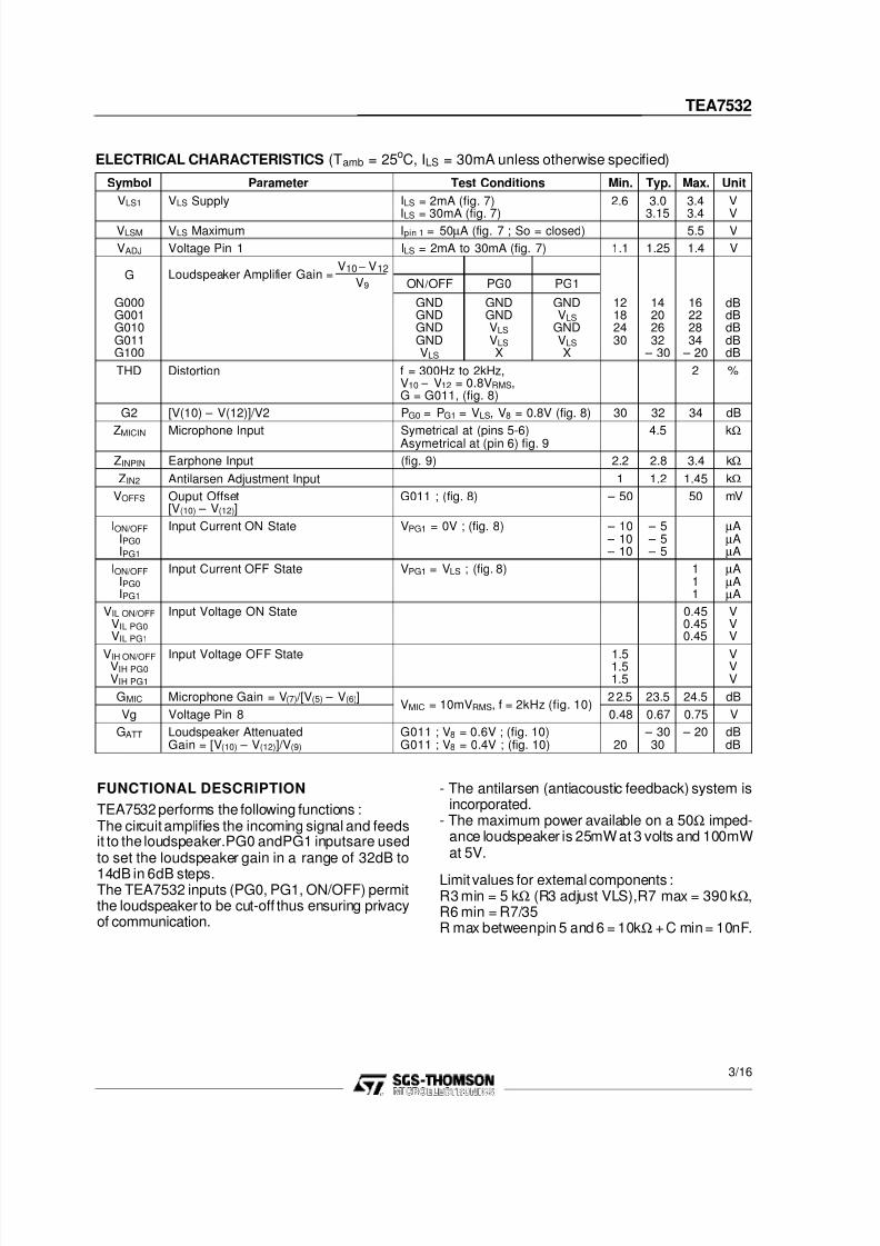
FUNCTIONAL DESCRIPTION
TEA7532 performs the following functions The circuit amplifies the incoming signal and feedsit to the loudspeakerPG0 andPG1 inputsare usedto set the loudspeaker gain in a range of 32dB to
14dB in 6dB stepsThe TEA7532 inputs (PG0 PG1 ONOFF) permitthe loudspeaker to be cut-off thus ensuring privacyof communication
- The antilarsen (antiacoustic feedback) system isincorporated
- The maximum power available on a 50Ω imped-ance loudspeaker is 25mW at 3 volts and 100mWat 5V
Limit values for external components R3 min = 5 kΩ (R3 adjust VLS)R7 max = 390 kΩR6 min = R735R max betweenpin 5 and 6 = 10kΩ + C min = 10nF
ELECTRICAL CHARACTERISTICS (Tamb = 25oC ILS = 30mA unless otherwise specified)
Symbol Parameter Test Conditions Min Typ Max Unit
VLS1 VLS Supply ILS = 2mA (fig 7)
ILS = 30mA (fig 7)
26 30
315
34
34
V
VVLSM VLS Maximum Ipin 1 = 50microA (fig 7 So = closed) 55 V
VADJ Voltage Pin 1 ILS = 2mA to 30mA (fig 7) 11 125 14 V
G Loudspeaker Amplifier Gain = V10minus V12
V9 ONOFF PG0 PG1
G000G001G010G011G100
GNDGNDGNDGNDVLS
GNDGNDVLS
VLS
X
GNDVLS
GNDVLS
X
12182430
14202632
ndash 30
16222834
ndash 20
dBdBdBdBdB
THD Distortion f = 300Hz to 2kHzV10 ndash V12 = 08VRMSG = G011 (fig 8)
2
G2 [V(10) ndash V(12)]V2 PG0 = PG1 = VLS V8 = 08V (fig 8) 30 32 34 dB
ZMICIN Microphone Input Symetrical at (pins 5-6)Asymetrical at (pin 6) fig 9 45 kΩ
ZINPIN Earphone Input (fig 9) 22 28 34 kΩ
ZIN2 Antilarsen Adjustment Input 1 12 145 kΩ
VOFFS Ouput Offset[V(10) ndash V(12)]
G011 (fig 8) ndash 50 50 mV
IONOFF
IPG0
IPG1
Input Current ON State VPG1 = 0V (fig 8) ndash 10 ndash 10 ndash 10
ndash 5 ndash 5 ndash 5
microAmicroAmicroA
IONOFF
IPG0
IPG1
Input Current OFF State VPG1 = VLS (fig 8) 111
microAmicroAmicroA
VIL ONOFF
VIL PG0
VIL PG1
Input Voltage ON State 045045045
VVV
VIH ONOFFVIH PG0
VIH PG1
Input Voltage OFF State 151515
VVV
GMIC Microphone Gain = V(7) [V(5) ndash V(6)]VMIC = 10mVRMS f = 2kHz (fig 10)
2 25 235 245 dB
Vg Voltage Pin 8 048 067 075 V
GATT Loudspeaker AttenuatedGain = [V(10) ndash V(12)]V(9)
G011 V8 = 06V (fig 10)G011 V8 = 04V (fig 10) 20
ndash 3030
ndash 20 dBdB
TEA7532
316
7252019 mXtwxytTDA
httpslidepdfcomreaderfullmxtwxyttda 417
Figure 1 LoudspeakerGain Versus Voltage onPin (3) - (8) with Pin 2 Open
Figure 3 AC Output Voltage Versus AmplifierGain
Figure 4 Power Available on LoudspeakerVersus VLS Typical Curve
Figure 2 LoudspeakerGain Versus Voltage onPin (3) - (8) and Versus R2 ()
Zin2 (12 K) R2 = 10 K rArr ATT = 20 dB() ATTENUATION =Zin2 (12 K) + R2 (E X T) R2 = 3 K rArr AT T asymp 10 dB
Figure 5 Distortion Versus Output Power Figure 6 Output Power Versus Supply Current
TEA7532
416
7252019 mXtwxytTDA
httpslidepdfcomreaderfullmxtwxyttda 517
TEST CIRCUITS
Figure 7 ShuntvoltageRegulator ReferenceVoltage at Pin 1
Note S0 open for VLS 1S0 close for VLSM
Figure 8 LoudspeakerAmplifier GainDistortionOutputOffset
V (10) ndash V (12) Voutbull G = =
V (9) V (9)
bull VOFFS with Vin = 0
VLS = 1GND = 0
Figure 9 Impedance ZMIC ZINP and Zin2
11 V 11 V 11 VZmic = Zinp = Zin2 =
I6 I9 I2
Figure 10 Antiacoustic Feedback System at
G011
S1 S2 S3
G1XX 1 X X
G000 0 0 0
G010 0 1 0
G001 0 0 1
TEA7532
516
7252019 mXtwxytTDA
httpslidepdfcomreaderfullmxtwxyttda 617
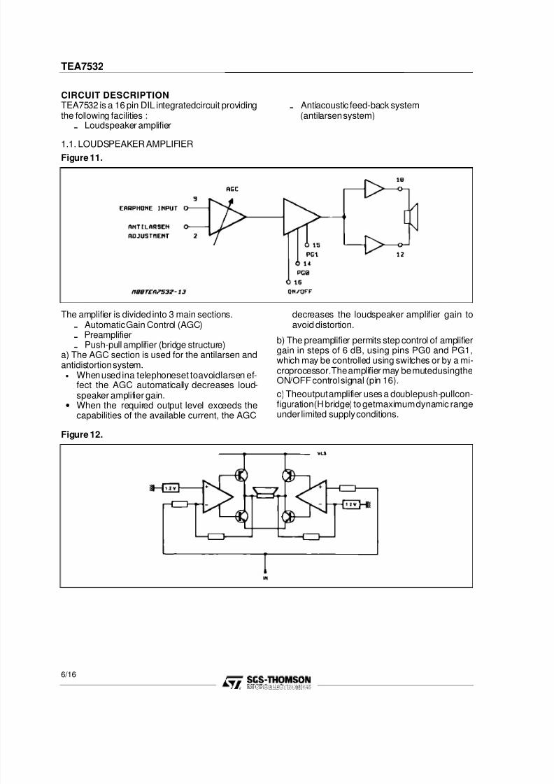
CIRCUIT DESCRIPTIONTEA7532 is a 16 pin DIL integratedcircuit providingthe following facilities
- Loudspeaker amplifier
- Antiacoustic feed-back system(antilarsen system)
11 LOUDSPEAKER AMPLIFIER
Figure 11
The amplifier is divided into 3 main sections
- AutomaticGain Control (AGC)
- Preamplifier
- Push-pull amplifier (bridge structure)a) The AGC section is used for the antilarsen andantidistortion systembull When used ina telephoneset toavoidlarsen ef-
fect the AGC automatically decreases loud-speaker amplifier gain
bull When the required output level exceeds thecapabilities of the available current the AGC
decreases the loudspeaker amplifier gain toavoid distortion
b) The preamplifier permits step control of amplifiergain in steps of 6 dB using pins PG0 and PG1which may be controlled using switches or by a mi-croprocessorThe amplifier may be mutedusingtheONOFF control signal (pin 16)
c) Theoutput amplifier uses a doublepush-pullcon-figuration(H bridge) to getmaximumdynamic range
under limited supply conditions
Figure 12
TEA7532
616
7252019 mXtwxytTDA
httpslidepdfcomreaderfullmxtwxyttda 717
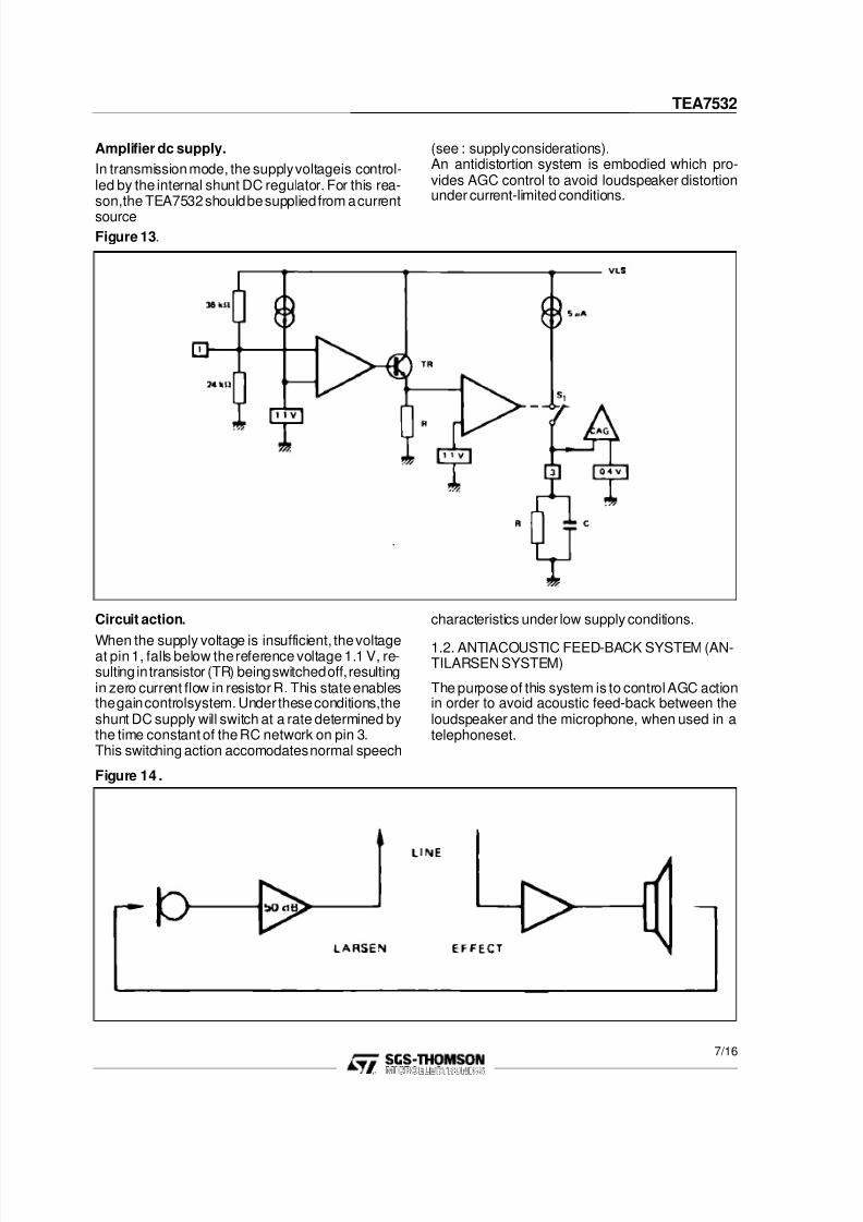
Amplifier dc supply
In transmission mode the supply voltageis control-led by the internal shunt DC regulator For this rea-sonthe TEA7532 should be supplied from a current
source
(see supplyconsiderations)An antidistortion system is embodied which pro-vides AGC control to avoid loudspeaker distortionunder current-limited conditions
Figure 13
Circuit action
When the supply voltage is insufficient the voltageat pin 1 falls below the reference voltage 11 V re-sulting in transistor (TR) being switched off resultingin zero current flow in resistor R This state enablesthe gain controlsystem Under these conditionstheshunt DC supply will switch at a rate determined bythe time constant of the RC network on pin 3This switching action accomodatesnormal speech
characteristics under low supply conditions
12 ANTIACOUSTIC FEED-BACK SYSTEM (AN-TILARSEN SYSTEM)
The purpose of this system is to control AGC actionin order to avoid acoustic feed-back between theloudspeaker and the microphone when used in atelephoneset
Figure 14
TEA7532
716
7252019 mXtwxytTDA
httpslidepdfcomreaderfullmxtwxyttda 817
Figure 15
Principle of operation
When examining the spectral density of the voicearea and the larsen area it can be seen that the
dominant features of each exist in different fre-quencybands
To extract the larsen component the microphonesignal is first filtered by a secondorder filter (formed
by two first order filters) then amplified and rectifiedin order to produce the AGC control signal
The first filter is generated by the capacitors on pins 5 and 6 the second filter by the R-C network on pin 7
Figure 16
Zin 4 kΩV7
A = = 15V5 ndash V6
TEA7532
816
7252019 mXtwxytTDA
httpslidepdfcomreaderfullmxtwxyttda 917
Figure 17 Antilarsen System Filter Response
Antilarsen system
Filter response
Filter on pins 5 amp 6
C9 + C10f2 =
2π Zin C9 C10
Filter on pin 7
1f1 =
2π (R5+ R6)C5
1f3 =
2π R5 C5
If f2 = f3 the Antilarsen system filter is equivalentto a second order filter
C9 + C10 1=
2π Zin C9 C10 2π R5C5
TEA7532
916
7252019 mXtwxytTDA
httpslidepdfcomreaderfullmxtwxyttda 1017
Figure 18
A complete telephone set has two antilarsensystems
- one in the transmission circuit (for example TEA7051)antisidetone network
- one in the loudspeaker amplifier(for example TEA7532)
Together these form a high efficiency antilarsensystem
PIN FUNCTIONS
PIN 1 ADJUST VLS
This pin is used to adjust the IC supply voltage
PIN 2 ANTILARSEN ADJUSTMENT
The AC signal at this pin is amplified to the loud-speaker without AGC attenuation
PIN 3 AUTOMATIC GAIN CONTROL FILTERThe antidistortion system response is adjusted bythe R-C network on this pinThe AGC will be switched ON when the level on pin3 is greaterthan thereference voltage (04V) theRC-network charges (current source ON) or discharges(current source OFF) accordingto thesupply voltage
TEA7532
1016
7252019 mXtwxytTDA
httpslidepdfcomreaderfullmxtwxyttda 1117
THEORETICAL VOLTAGE ON PIN 3
Figure 19
- The value of R affects the system time constantand the chargedischarge duty cycle
- The value of C only affectsthe system time con-stant
- R shouldbe greateror equalthan 150kΩ forcor-rect AGC operation
Figure 20
PIN 4 CIRCUIT SUPPLY VOLTAGEWith pin1 open circuit VLS is internally stabilized at28 V
Whenthe TEA7532is underAGCcontrol thevoltageon this pin varies slightly (due to AGC action)
TEA7532
1116
7252019 mXtwxytTDA
httpslidepdfcomreaderfullmxtwxyttda 1217
PIN 56 MICROPHONE INPUTS
These are used for antilarsen control
PIN 7 ANTILARSEN FILTER 1
The second filter of the antilarsen system (1 st filter pins 5-6) is formed by the RC network R5C5In order to obtain a second order filter for the anti-larsen system the cut-off frequency defined at thispin should be the same as that chosen for the firstfilter
For correct TEA7532 operation R6 and R5 shouldbe fixed at 10 kΩ and 1 kΩ respectively
PIN 8 ANTILARSEN FILTER 2
The gain and the response of the antilarsen systemcan be adjusted respectively by the resistor and the
capacitor onthis pin according to the acousticchar-acteristics of the telephone set
The value of the resistor should not exceed 390 kΩWhen the voltage on this pin exceeds the thresholdvoltage of 04 V the AGC system is enabled
PIN 9 EARPHONE INPUT
Input for loudspeaker signal
PIN 10-12 LOUDSPEAKER OUTPUTS
Maximum output voltage Vpp = 2 VLS - 25 V (witha gain of 32 dB)
Maximum output current depending of the supplycurrent
Two loudspeakerconnection methods are possibleusing the amplifier in either rdquoHrdquo mode or rdquoBrdquo mode
Note It is advisable to connect a 47 nF capacitorin parallel with the loudspeaker (betweenpins 10 and 12)
- rdquoHrdquo Mode
This is for low voltage working butat a higher supply
current The highest output power is available in thismode due to the 55V maximum supply voltage re-striction imposed by the TEA7532Loudspeakerimpedancerecommendedvalue 50ΩMaximum gain available between earphone inputand loudspeaker output 32 dB
Figure 21
Figure 22
TEA7532
1216
7252019 mXtwxytTDA
httpslidepdfcomreaderfullmxtwxyttda 1317
- rdquoBrdquo ModeThis allows higher voltage operation but at a lowersupply currentLoudspeakerimpedancerecommendedvalue 25Ω
Maximum gain available between earphone inputand loudspeaker output 32 - 6 = 26 dB
PIN 11 Vref INTERNAL REFERENCEOutput which provides an internally regulated refer-ence voltage
Vref = 11 V typical
MAXIMUM AVAILABLE CURRENT 5 microA
Figure 23
PIN 13 GROUND
PIN 14-15 GAIN ADJUSTMENT INPUTS
These pins are used to adjust the loudspeaker am-plifier gain Four steps of 6 dBstep are available(pin open circuit = high level)
PIN 16 LOUDSPEAKER MUTING
This pin is used to mute the loudspeaker Pin open-
circuit high level = loudspeaker mutedPin low level louspeaker enabled (see connectionof pins 14 and 15)
PG0 PG1
1 1 Gmax
1 0 Gmax - lt0gt 6 dB
0 1 Gmax - 12 dB
0 0 Gmax - 18 dB
TEA7532
1316
7252019 mXtwxytTDA
httpslidepdfcomreaderfullmxtwxyttda 1417
16
1 8
I a 1
L
B e
D
bZ
e3
F
b1
E
9
P M - D I P 1 6 E
P S
DIP16 PACKAGE MECHANICAL DATA
DIMmm inch
Min Typ Max Min Typ Max
a1 051 0020
B 077 165 0030 0065
b 05 0020
b1 025 0010
D 20 0787
E 85 0335
e 254 0100
e3 1778 0700
F 71 0280
i 51 0201
L 33 0130
Z 127 0050
D I P 1 6 T
B L
TEA7532
1416
7252019 mXtwxytTDA
httpslidepdfcomreaderfullmxtwxyttda 1517
b 1
c1
s
F
C
GL
E
a 1
a 2
A
e
DM
e3
b
16 9
1 8
P M - S O 1 6 E
P S
SO16 PACKAGE MECHANICAL DATA
DimensionsMillimeters Inches
Min Typ Max Min Typ Max
A 175 0069
a1 01 02 0004 0008
a2 16 0063
b 035 046 0014 0018
b1 019 025 0007 0010
C 05 0020
c1 45o (typ)
D 98 10 0386 0394
E 58 62 0228 0244
e 127 0050
e3 889 0350
F 38 40 0150 0157
G 46 53 0181 0209
L 05 127 0020 0050
M 062 0024
S 8o
(max)
S O 1 6 T
B L
TEA7532
1516
7252019 mXtwxytTDA
httpslidepdfcomreaderfullmxtwxyttda 1617
Information furnished is believed to be accurate and reli able However SGS-THOMSON Microelectronics assumes no responsibility for
the consequences of use of such information nor for any infringement of patents or other rights of third parties which may result from itsuse No license is granted by implication or otherwise under any patent or patent rights of SGS-THOMSON Microelectronics Specifica-tions mentioned i n this publication are subject to change w ithout notice This publication supersedes and replaces all information pre-
viously supplied SGS-THOMSON Microelectronics products are not authorized for use as critical components in l ife support devices orsystems without express written approval of SGS-THOMSON Microelectronics
983209 1994 SGS-THOMSON Microelectronics - All Rights Reserved
SGS-THOMSON Microelectronics GROUP OF COMPANIES
Australia - Brazil - France - Germany - Hong Kong - Italy - Japan - Korea - Malaysia - Malta - Morocco - The NetherlandsSingapore - Spain - Sweden - Switzerland - Taiwan - Thaliand - United Kingdom- USA
TEA7532
1616
7252019 mXtwxytTDA
httpslidepdfcomreaderfullmxtwxyttda 1717
This datasheet has been download from
wwwdatasheetcatalogcom
Datasheets for electronics components
7252019 mXtwxytTDA
httpslidepdfcomreaderfullmxtwxyttda 217
PIN DESCRIPTION
Ndeg Symbol Description
1 ADJ Adjust Internal Reference VLS
2 ALADJ Antilarsen Adjustement
3 ADS Antidistortion
4 VLS Supply
5 MIC1 Microphone Input
6 MIC2 Microphone input
7 FAL Antilarsen Filter
8 TC1 Antilarsen Time Constant
9 INP Input Signal
10 LS1 Output Loudspeaker 1
11 VREF Internal Resistance
12 LS2 Output Loudspeaker 2
13 GND Ground
141516
PG0PG1
ONOFFInputs Program Level to Loudspeaker
PIN CONNECTION (Top view)
ABSOLUTE MAXIMUM RATINGS
Symbol Parameter Value Unit
Top Temperature Range ndash5 to + 45 degC
VLS Supply Voltage 6 V
ILS Supply Current for T gt 300msfor T le 300ms
90150
mAmA
VL Voltage Level (pins PG0 PG1 onoff) 06 gt to VS + 06 V
TEA7532
216
7252019 mXtwxytTDA
httpslidepdfcomreaderfullmxtwxyttda 317
FUNCTIONAL DESCRIPTION
TEA7532 performs the following functions The circuit amplifies the incoming signal and feedsit to the loudspeakerPG0 andPG1 inputsare usedto set the loudspeaker gain in a range of 32dB to
14dB in 6dB stepsThe TEA7532 inputs (PG0 PG1 ONOFF) permitthe loudspeaker to be cut-off thus ensuring privacyof communication
- The antilarsen (antiacoustic feedback) system isincorporated
- The maximum power available on a 50Ω imped-ance loudspeaker is 25mW at 3 volts and 100mWat 5V
Limit values for external components R3 min = 5 kΩ (R3 adjust VLS)R7 max = 390 kΩR6 min = R735R max betweenpin 5 and 6 = 10kΩ + C min = 10nF
ELECTRICAL CHARACTERISTICS (Tamb = 25oC ILS = 30mA unless otherwise specified)
Symbol Parameter Test Conditions Min Typ Max Unit
VLS1 VLS Supply ILS = 2mA (fig 7)
ILS = 30mA (fig 7)
26 30
315
34
34
V
VVLSM VLS Maximum Ipin 1 = 50microA (fig 7 So = closed) 55 V
VADJ Voltage Pin 1 ILS = 2mA to 30mA (fig 7) 11 125 14 V
G Loudspeaker Amplifier Gain = V10minus V12
V9 ONOFF PG0 PG1
G000G001G010G011G100
GNDGNDGNDGNDVLS
GNDGNDVLS
VLS
X
GNDVLS
GNDVLS
X
12182430
14202632
ndash 30
16222834
ndash 20
dBdBdBdBdB
THD Distortion f = 300Hz to 2kHzV10 ndash V12 = 08VRMSG = G011 (fig 8)
2
G2 [V(10) ndash V(12)]V2 PG0 = PG1 = VLS V8 = 08V (fig 8) 30 32 34 dB
ZMICIN Microphone Input Symetrical at (pins 5-6)Asymetrical at (pin 6) fig 9 45 kΩ
ZINPIN Earphone Input (fig 9) 22 28 34 kΩ
ZIN2 Antilarsen Adjustment Input 1 12 145 kΩ
VOFFS Ouput Offset[V(10) ndash V(12)]
G011 (fig 8) ndash 50 50 mV
IONOFF
IPG0
IPG1
Input Current ON State VPG1 = 0V (fig 8) ndash 10 ndash 10 ndash 10
ndash 5 ndash 5 ndash 5
microAmicroAmicroA
IONOFF
IPG0
IPG1
Input Current OFF State VPG1 = VLS (fig 8) 111
microAmicroAmicroA
VIL ONOFF
VIL PG0
VIL PG1
Input Voltage ON State 045045045
VVV
VIH ONOFFVIH PG0
VIH PG1
Input Voltage OFF State 151515
VVV
GMIC Microphone Gain = V(7) [V(5) ndash V(6)]VMIC = 10mVRMS f = 2kHz (fig 10)
2 25 235 245 dB
Vg Voltage Pin 8 048 067 075 V
GATT Loudspeaker AttenuatedGain = [V(10) ndash V(12)]V(9)
G011 V8 = 06V (fig 10)G011 V8 = 04V (fig 10) 20
ndash 3030
ndash 20 dBdB
TEA7532
316
7252019 mXtwxytTDA
httpslidepdfcomreaderfullmxtwxyttda 417
Figure 1 LoudspeakerGain Versus Voltage onPin (3) - (8) with Pin 2 Open
Figure 3 AC Output Voltage Versus AmplifierGain
Figure 4 Power Available on LoudspeakerVersus VLS Typical Curve
Figure 2 LoudspeakerGain Versus Voltage onPin (3) - (8) and Versus R2 ()
Zin2 (12 K) R2 = 10 K rArr ATT = 20 dB() ATTENUATION =Zin2 (12 K) + R2 (E X T) R2 = 3 K rArr AT T asymp 10 dB
Figure 5 Distortion Versus Output Power Figure 6 Output Power Versus Supply Current
TEA7532
416
7252019 mXtwxytTDA
httpslidepdfcomreaderfullmxtwxyttda 517
TEST CIRCUITS
Figure 7 ShuntvoltageRegulator ReferenceVoltage at Pin 1
Note S0 open for VLS 1S0 close for VLSM
Figure 8 LoudspeakerAmplifier GainDistortionOutputOffset
V (10) ndash V (12) Voutbull G = =
V (9) V (9)
bull VOFFS with Vin = 0
VLS = 1GND = 0
Figure 9 Impedance ZMIC ZINP and Zin2
11 V 11 V 11 VZmic = Zinp = Zin2 =
I6 I9 I2
Figure 10 Antiacoustic Feedback System at
G011
S1 S2 S3
G1XX 1 X X
G000 0 0 0
G010 0 1 0
G001 0 0 1
TEA7532
516
7252019 mXtwxytTDA
httpslidepdfcomreaderfullmxtwxyttda 617
CIRCUIT DESCRIPTIONTEA7532 is a 16 pin DIL integratedcircuit providingthe following facilities
- Loudspeaker amplifier
- Antiacoustic feed-back system(antilarsen system)
11 LOUDSPEAKER AMPLIFIER
Figure 11
The amplifier is divided into 3 main sections
- AutomaticGain Control (AGC)
- Preamplifier
- Push-pull amplifier (bridge structure)a) The AGC section is used for the antilarsen andantidistortion systembull When used ina telephoneset toavoidlarsen ef-
fect the AGC automatically decreases loud-speaker amplifier gain
bull When the required output level exceeds thecapabilities of the available current the AGC
decreases the loudspeaker amplifier gain toavoid distortion
b) The preamplifier permits step control of amplifiergain in steps of 6 dB using pins PG0 and PG1which may be controlled using switches or by a mi-croprocessorThe amplifier may be mutedusingtheONOFF control signal (pin 16)
c) Theoutput amplifier uses a doublepush-pullcon-figuration(H bridge) to getmaximumdynamic range
under limited supply conditions
Figure 12
TEA7532
616
7252019 mXtwxytTDA
httpslidepdfcomreaderfullmxtwxyttda 717
Amplifier dc supply
In transmission mode the supply voltageis control-led by the internal shunt DC regulator For this rea-sonthe TEA7532 should be supplied from a current
source
(see supplyconsiderations)An antidistortion system is embodied which pro-vides AGC control to avoid loudspeaker distortionunder current-limited conditions
Figure 13
Circuit action
When the supply voltage is insufficient the voltageat pin 1 falls below the reference voltage 11 V re-sulting in transistor (TR) being switched off resultingin zero current flow in resistor R This state enablesthe gain controlsystem Under these conditionstheshunt DC supply will switch at a rate determined bythe time constant of the RC network on pin 3This switching action accomodatesnormal speech
characteristics under low supply conditions
12 ANTIACOUSTIC FEED-BACK SYSTEM (AN-TILARSEN SYSTEM)
The purpose of this system is to control AGC actionin order to avoid acoustic feed-back between theloudspeaker and the microphone when used in atelephoneset
Figure 14
TEA7532
716
7252019 mXtwxytTDA
httpslidepdfcomreaderfullmxtwxyttda 817
Figure 15
Principle of operation
When examining the spectral density of the voicearea and the larsen area it can be seen that the
dominant features of each exist in different fre-quencybands
To extract the larsen component the microphonesignal is first filtered by a secondorder filter (formed
by two first order filters) then amplified and rectifiedin order to produce the AGC control signal
The first filter is generated by the capacitors on pins 5 and 6 the second filter by the R-C network on pin 7
Figure 16
Zin 4 kΩV7
A = = 15V5 ndash V6
TEA7532
816
7252019 mXtwxytTDA
httpslidepdfcomreaderfullmxtwxyttda 917
Figure 17 Antilarsen System Filter Response
Antilarsen system
Filter response
Filter on pins 5 amp 6
C9 + C10f2 =
2π Zin C9 C10
Filter on pin 7
1f1 =
2π (R5+ R6)C5
1f3 =
2π R5 C5
If f2 = f3 the Antilarsen system filter is equivalentto a second order filter
C9 + C10 1=
2π Zin C9 C10 2π R5C5
TEA7532
916
7252019 mXtwxytTDA
httpslidepdfcomreaderfullmxtwxyttda 1017
Figure 18
A complete telephone set has two antilarsensystems
- one in the transmission circuit (for example TEA7051)antisidetone network
- one in the loudspeaker amplifier(for example TEA7532)
Together these form a high efficiency antilarsensystem
PIN FUNCTIONS
PIN 1 ADJUST VLS
This pin is used to adjust the IC supply voltage
PIN 2 ANTILARSEN ADJUSTMENT
The AC signal at this pin is amplified to the loud-speaker without AGC attenuation
PIN 3 AUTOMATIC GAIN CONTROL FILTERThe antidistortion system response is adjusted bythe R-C network on this pinThe AGC will be switched ON when the level on pin3 is greaterthan thereference voltage (04V) theRC-network charges (current source ON) or discharges(current source OFF) accordingto thesupply voltage
TEA7532
1016
7252019 mXtwxytTDA
httpslidepdfcomreaderfullmxtwxyttda 1117
THEORETICAL VOLTAGE ON PIN 3
Figure 19
- The value of R affects the system time constantand the chargedischarge duty cycle
- The value of C only affectsthe system time con-stant
- R shouldbe greateror equalthan 150kΩ forcor-rect AGC operation
Figure 20
PIN 4 CIRCUIT SUPPLY VOLTAGEWith pin1 open circuit VLS is internally stabilized at28 V
Whenthe TEA7532is underAGCcontrol thevoltageon this pin varies slightly (due to AGC action)
TEA7532
1116
7252019 mXtwxytTDA
httpslidepdfcomreaderfullmxtwxyttda 1217
PIN 56 MICROPHONE INPUTS
These are used for antilarsen control
PIN 7 ANTILARSEN FILTER 1
The second filter of the antilarsen system (1 st filter pins 5-6) is formed by the RC network R5C5In order to obtain a second order filter for the anti-larsen system the cut-off frequency defined at thispin should be the same as that chosen for the firstfilter
For correct TEA7532 operation R6 and R5 shouldbe fixed at 10 kΩ and 1 kΩ respectively
PIN 8 ANTILARSEN FILTER 2
The gain and the response of the antilarsen systemcan be adjusted respectively by the resistor and the
capacitor onthis pin according to the acousticchar-acteristics of the telephone set
The value of the resistor should not exceed 390 kΩWhen the voltage on this pin exceeds the thresholdvoltage of 04 V the AGC system is enabled
PIN 9 EARPHONE INPUT
Input for loudspeaker signal
PIN 10-12 LOUDSPEAKER OUTPUTS
Maximum output voltage Vpp = 2 VLS - 25 V (witha gain of 32 dB)
Maximum output current depending of the supplycurrent
Two loudspeakerconnection methods are possibleusing the amplifier in either rdquoHrdquo mode or rdquoBrdquo mode
Note It is advisable to connect a 47 nF capacitorin parallel with the loudspeaker (betweenpins 10 and 12)
- rdquoHrdquo Mode
This is for low voltage working butat a higher supply
current The highest output power is available in thismode due to the 55V maximum supply voltage re-striction imposed by the TEA7532Loudspeakerimpedancerecommendedvalue 50ΩMaximum gain available between earphone inputand loudspeaker output 32 dB
Figure 21
Figure 22
TEA7532
1216
7252019 mXtwxytTDA
httpslidepdfcomreaderfullmxtwxyttda 1317
- rdquoBrdquo ModeThis allows higher voltage operation but at a lowersupply currentLoudspeakerimpedancerecommendedvalue 25Ω
Maximum gain available between earphone inputand loudspeaker output 32 - 6 = 26 dB
PIN 11 Vref INTERNAL REFERENCEOutput which provides an internally regulated refer-ence voltage
Vref = 11 V typical
MAXIMUM AVAILABLE CURRENT 5 microA
Figure 23
PIN 13 GROUND
PIN 14-15 GAIN ADJUSTMENT INPUTS
These pins are used to adjust the loudspeaker am-plifier gain Four steps of 6 dBstep are available(pin open circuit = high level)
PIN 16 LOUDSPEAKER MUTING
This pin is used to mute the loudspeaker Pin open-
circuit high level = loudspeaker mutedPin low level louspeaker enabled (see connectionof pins 14 and 15)
PG0 PG1
1 1 Gmax
1 0 Gmax - lt0gt 6 dB
0 1 Gmax - 12 dB
0 0 Gmax - 18 dB
TEA7532
1316
7252019 mXtwxytTDA
httpslidepdfcomreaderfullmxtwxyttda 1417
16
1 8
I a 1
L
B e
D
bZ
e3
F
b1
E
9
P M - D I P 1 6 E
P S
DIP16 PACKAGE MECHANICAL DATA
DIMmm inch
Min Typ Max Min Typ Max
a1 051 0020
B 077 165 0030 0065
b 05 0020
b1 025 0010
D 20 0787
E 85 0335
e 254 0100
e3 1778 0700
F 71 0280
i 51 0201
L 33 0130
Z 127 0050
D I P 1 6 T
B L
TEA7532
1416
7252019 mXtwxytTDA
httpslidepdfcomreaderfullmxtwxyttda 1517
b 1
c1
s
F
C
GL
E
a 1
a 2
A
e
DM
e3
b
16 9
1 8
P M - S O 1 6 E
P S
SO16 PACKAGE MECHANICAL DATA
DimensionsMillimeters Inches
Min Typ Max Min Typ Max
A 175 0069
a1 01 02 0004 0008
a2 16 0063
b 035 046 0014 0018
b1 019 025 0007 0010
C 05 0020
c1 45o (typ)
D 98 10 0386 0394
E 58 62 0228 0244
e 127 0050
e3 889 0350
F 38 40 0150 0157
G 46 53 0181 0209
L 05 127 0020 0050
M 062 0024
S 8o
(max)
S O 1 6 T
B L
TEA7532
1516
7252019 mXtwxytTDA
httpslidepdfcomreaderfullmxtwxyttda 1617
Information furnished is believed to be accurate and reli able However SGS-THOMSON Microelectronics assumes no responsibility for
the consequences of use of such information nor for any infringement of patents or other rights of third parties which may result from itsuse No license is granted by implication or otherwise under any patent or patent rights of SGS-THOMSON Microelectronics Specifica-tions mentioned i n this publication are subject to change w ithout notice This publication supersedes and replaces all information pre-
viously supplied SGS-THOMSON Microelectronics products are not authorized for use as critical components in l ife support devices orsystems without express written approval of SGS-THOMSON Microelectronics
983209 1994 SGS-THOMSON Microelectronics - All Rights Reserved
SGS-THOMSON Microelectronics GROUP OF COMPANIES
Australia - Brazil - France - Germany - Hong Kong - Italy - Japan - Korea - Malaysia - Malta - Morocco - The NetherlandsSingapore - Spain - Sweden - Switzerland - Taiwan - Thaliand - United Kingdom- USA
TEA7532
1616
7252019 mXtwxytTDA
httpslidepdfcomreaderfullmxtwxyttda 1717
This datasheet has been download from
wwwdatasheetcatalogcom
Datasheets for electronics components
7252019 mXtwxytTDA
httpslidepdfcomreaderfullmxtwxyttda 317
FUNCTIONAL DESCRIPTION
TEA7532 performs the following functions The circuit amplifies the incoming signal and feedsit to the loudspeakerPG0 andPG1 inputsare usedto set the loudspeaker gain in a range of 32dB to
14dB in 6dB stepsThe TEA7532 inputs (PG0 PG1 ONOFF) permitthe loudspeaker to be cut-off thus ensuring privacyof communication
- The antilarsen (antiacoustic feedback) system isincorporated
- The maximum power available on a 50Ω imped-ance loudspeaker is 25mW at 3 volts and 100mWat 5V
Limit values for external components R3 min = 5 kΩ (R3 adjust VLS)R7 max = 390 kΩR6 min = R735R max betweenpin 5 and 6 = 10kΩ + C min = 10nF
ELECTRICAL CHARACTERISTICS (Tamb = 25oC ILS = 30mA unless otherwise specified)
Symbol Parameter Test Conditions Min Typ Max Unit
VLS1 VLS Supply ILS = 2mA (fig 7)
ILS = 30mA (fig 7)
26 30
315
34
34
V
VVLSM VLS Maximum Ipin 1 = 50microA (fig 7 So = closed) 55 V
VADJ Voltage Pin 1 ILS = 2mA to 30mA (fig 7) 11 125 14 V
G Loudspeaker Amplifier Gain = V10minus V12
V9 ONOFF PG0 PG1
G000G001G010G011G100
GNDGNDGNDGNDVLS
GNDGNDVLS
VLS
X
GNDVLS
GNDVLS
X
12182430
14202632
ndash 30
16222834
ndash 20
dBdBdBdBdB
THD Distortion f = 300Hz to 2kHzV10 ndash V12 = 08VRMSG = G011 (fig 8)
2
G2 [V(10) ndash V(12)]V2 PG0 = PG1 = VLS V8 = 08V (fig 8) 30 32 34 dB
ZMICIN Microphone Input Symetrical at (pins 5-6)Asymetrical at (pin 6) fig 9 45 kΩ
ZINPIN Earphone Input (fig 9) 22 28 34 kΩ
ZIN2 Antilarsen Adjustment Input 1 12 145 kΩ
VOFFS Ouput Offset[V(10) ndash V(12)]
G011 (fig 8) ndash 50 50 mV
IONOFF
IPG0
IPG1
Input Current ON State VPG1 = 0V (fig 8) ndash 10 ndash 10 ndash 10
ndash 5 ndash 5 ndash 5
microAmicroAmicroA
IONOFF
IPG0
IPG1
Input Current OFF State VPG1 = VLS (fig 8) 111
microAmicroAmicroA
VIL ONOFF
VIL PG0
VIL PG1
Input Voltage ON State 045045045
VVV
VIH ONOFFVIH PG0
VIH PG1
Input Voltage OFF State 151515
VVV
GMIC Microphone Gain = V(7) [V(5) ndash V(6)]VMIC = 10mVRMS f = 2kHz (fig 10)
2 25 235 245 dB
Vg Voltage Pin 8 048 067 075 V
GATT Loudspeaker AttenuatedGain = [V(10) ndash V(12)]V(9)
G011 V8 = 06V (fig 10)G011 V8 = 04V (fig 10) 20
ndash 3030
ndash 20 dBdB
TEA7532
316
7252019 mXtwxytTDA
httpslidepdfcomreaderfullmxtwxyttda 417
Figure 1 LoudspeakerGain Versus Voltage onPin (3) - (8) with Pin 2 Open
Figure 3 AC Output Voltage Versus AmplifierGain
Figure 4 Power Available on LoudspeakerVersus VLS Typical Curve
Figure 2 LoudspeakerGain Versus Voltage onPin (3) - (8) and Versus R2 ()
Zin2 (12 K) R2 = 10 K rArr ATT = 20 dB() ATTENUATION =Zin2 (12 K) + R2 (E X T) R2 = 3 K rArr AT T asymp 10 dB
Figure 5 Distortion Versus Output Power Figure 6 Output Power Versus Supply Current
TEA7532
416
7252019 mXtwxytTDA
httpslidepdfcomreaderfullmxtwxyttda 517
TEST CIRCUITS
Figure 7 ShuntvoltageRegulator ReferenceVoltage at Pin 1
Note S0 open for VLS 1S0 close for VLSM
Figure 8 LoudspeakerAmplifier GainDistortionOutputOffset
V (10) ndash V (12) Voutbull G = =
V (9) V (9)
bull VOFFS with Vin = 0
VLS = 1GND = 0
Figure 9 Impedance ZMIC ZINP and Zin2
11 V 11 V 11 VZmic = Zinp = Zin2 =
I6 I9 I2
Figure 10 Antiacoustic Feedback System at
G011
S1 S2 S3
G1XX 1 X X
G000 0 0 0
G010 0 1 0
G001 0 0 1
TEA7532
516
7252019 mXtwxytTDA
httpslidepdfcomreaderfullmxtwxyttda 617
CIRCUIT DESCRIPTIONTEA7532 is a 16 pin DIL integratedcircuit providingthe following facilities
- Loudspeaker amplifier
- Antiacoustic feed-back system(antilarsen system)
11 LOUDSPEAKER AMPLIFIER
Figure 11
The amplifier is divided into 3 main sections
- AutomaticGain Control (AGC)
- Preamplifier
- Push-pull amplifier (bridge structure)a) The AGC section is used for the antilarsen andantidistortion systembull When used ina telephoneset toavoidlarsen ef-
fect the AGC automatically decreases loud-speaker amplifier gain
bull When the required output level exceeds thecapabilities of the available current the AGC
decreases the loudspeaker amplifier gain toavoid distortion
b) The preamplifier permits step control of amplifiergain in steps of 6 dB using pins PG0 and PG1which may be controlled using switches or by a mi-croprocessorThe amplifier may be mutedusingtheONOFF control signal (pin 16)
c) Theoutput amplifier uses a doublepush-pullcon-figuration(H bridge) to getmaximumdynamic range
under limited supply conditions
Figure 12
TEA7532
616
7252019 mXtwxytTDA
httpslidepdfcomreaderfullmxtwxyttda 717
Amplifier dc supply
In transmission mode the supply voltageis control-led by the internal shunt DC regulator For this rea-sonthe TEA7532 should be supplied from a current
source
(see supplyconsiderations)An antidistortion system is embodied which pro-vides AGC control to avoid loudspeaker distortionunder current-limited conditions
Figure 13
Circuit action
When the supply voltage is insufficient the voltageat pin 1 falls below the reference voltage 11 V re-sulting in transistor (TR) being switched off resultingin zero current flow in resistor R This state enablesthe gain controlsystem Under these conditionstheshunt DC supply will switch at a rate determined bythe time constant of the RC network on pin 3This switching action accomodatesnormal speech
characteristics under low supply conditions
12 ANTIACOUSTIC FEED-BACK SYSTEM (AN-TILARSEN SYSTEM)
The purpose of this system is to control AGC actionin order to avoid acoustic feed-back between theloudspeaker and the microphone when used in atelephoneset
Figure 14
TEA7532
716
7252019 mXtwxytTDA
httpslidepdfcomreaderfullmxtwxyttda 817
Figure 15
Principle of operation
When examining the spectral density of the voicearea and the larsen area it can be seen that the
dominant features of each exist in different fre-quencybands
To extract the larsen component the microphonesignal is first filtered by a secondorder filter (formed
by two first order filters) then amplified and rectifiedin order to produce the AGC control signal
The first filter is generated by the capacitors on pins 5 and 6 the second filter by the R-C network on pin 7
Figure 16
Zin 4 kΩV7
A = = 15V5 ndash V6
TEA7532
816
7252019 mXtwxytTDA
httpslidepdfcomreaderfullmxtwxyttda 917
Figure 17 Antilarsen System Filter Response
Antilarsen system
Filter response
Filter on pins 5 amp 6
C9 + C10f2 =
2π Zin C9 C10
Filter on pin 7
1f1 =
2π (R5+ R6)C5
1f3 =
2π R5 C5
If f2 = f3 the Antilarsen system filter is equivalentto a second order filter
C9 + C10 1=
2π Zin C9 C10 2π R5C5
TEA7532
916
7252019 mXtwxytTDA
httpslidepdfcomreaderfullmxtwxyttda 1017
Figure 18
A complete telephone set has two antilarsensystems
- one in the transmission circuit (for example TEA7051)antisidetone network
- one in the loudspeaker amplifier(for example TEA7532)
Together these form a high efficiency antilarsensystem
PIN FUNCTIONS
PIN 1 ADJUST VLS
This pin is used to adjust the IC supply voltage
PIN 2 ANTILARSEN ADJUSTMENT
The AC signal at this pin is amplified to the loud-speaker without AGC attenuation
PIN 3 AUTOMATIC GAIN CONTROL FILTERThe antidistortion system response is adjusted bythe R-C network on this pinThe AGC will be switched ON when the level on pin3 is greaterthan thereference voltage (04V) theRC-network charges (current source ON) or discharges(current source OFF) accordingto thesupply voltage
TEA7532
1016
7252019 mXtwxytTDA
httpslidepdfcomreaderfullmxtwxyttda 1117
THEORETICAL VOLTAGE ON PIN 3
Figure 19
- The value of R affects the system time constantand the chargedischarge duty cycle
- The value of C only affectsthe system time con-stant
- R shouldbe greateror equalthan 150kΩ forcor-rect AGC operation
Figure 20
PIN 4 CIRCUIT SUPPLY VOLTAGEWith pin1 open circuit VLS is internally stabilized at28 V
Whenthe TEA7532is underAGCcontrol thevoltageon this pin varies slightly (due to AGC action)
TEA7532
1116
7252019 mXtwxytTDA
httpslidepdfcomreaderfullmxtwxyttda 1217
PIN 56 MICROPHONE INPUTS
These are used for antilarsen control
PIN 7 ANTILARSEN FILTER 1
The second filter of the antilarsen system (1 st filter pins 5-6) is formed by the RC network R5C5In order to obtain a second order filter for the anti-larsen system the cut-off frequency defined at thispin should be the same as that chosen for the firstfilter
For correct TEA7532 operation R6 and R5 shouldbe fixed at 10 kΩ and 1 kΩ respectively
PIN 8 ANTILARSEN FILTER 2
The gain and the response of the antilarsen systemcan be adjusted respectively by the resistor and the
capacitor onthis pin according to the acousticchar-acteristics of the telephone set
The value of the resistor should not exceed 390 kΩWhen the voltage on this pin exceeds the thresholdvoltage of 04 V the AGC system is enabled
PIN 9 EARPHONE INPUT
Input for loudspeaker signal
PIN 10-12 LOUDSPEAKER OUTPUTS
Maximum output voltage Vpp = 2 VLS - 25 V (witha gain of 32 dB)
Maximum output current depending of the supplycurrent
Two loudspeakerconnection methods are possibleusing the amplifier in either rdquoHrdquo mode or rdquoBrdquo mode
Note It is advisable to connect a 47 nF capacitorin parallel with the loudspeaker (betweenpins 10 and 12)
- rdquoHrdquo Mode
This is for low voltage working butat a higher supply
current The highest output power is available in thismode due to the 55V maximum supply voltage re-striction imposed by the TEA7532Loudspeakerimpedancerecommendedvalue 50ΩMaximum gain available between earphone inputand loudspeaker output 32 dB
Figure 21
Figure 22
TEA7532
1216
7252019 mXtwxytTDA
httpslidepdfcomreaderfullmxtwxyttda 1317
- rdquoBrdquo ModeThis allows higher voltage operation but at a lowersupply currentLoudspeakerimpedancerecommendedvalue 25Ω
Maximum gain available between earphone inputand loudspeaker output 32 - 6 = 26 dB
PIN 11 Vref INTERNAL REFERENCEOutput which provides an internally regulated refer-ence voltage
Vref = 11 V typical
MAXIMUM AVAILABLE CURRENT 5 microA
Figure 23
PIN 13 GROUND
PIN 14-15 GAIN ADJUSTMENT INPUTS
These pins are used to adjust the loudspeaker am-plifier gain Four steps of 6 dBstep are available(pin open circuit = high level)
PIN 16 LOUDSPEAKER MUTING
This pin is used to mute the loudspeaker Pin open-
circuit high level = loudspeaker mutedPin low level louspeaker enabled (see connectionof pins 14 and 15)
PG0 PG1
1 1 Gmax
1 0 Gmax - lt0gt 6 dB
0 1 Gmax - 12 dB
0 0 Gmax - 18 dB
TEA7532
1316
7252019 mXtwxytTDA
httpslidepdfcomreaderfullmxtwxyttda 1417
16
1 8
I a 1
L
B e
D
bZ
e3
F
b1
E
9
P M - D I P 1 6 E
P S
DIP16 PACKAGE MECHANICAL DATA
DIMmm inch
Min Typ Max Min Typ Max
a1 051 0020
B 077 165 0030 0065
b 05 0020
b1 025 0010
D 20 0787
E 85 0335
e 254 0100
e3 1778 0700
F 71 0280
i 51 0201
L 33 0130
Z 127 0050
D I P 1 6 T
B L
TEA7532
1416
7252019 mXtwxytTDA
httpslidepdfcomreaderfullmxtwxyttda 1517
b 1
c1
s
F
C
GL
E
a 1
a 2
A
e
DM
e3
b
16 9
1 8
P M - S O 1 6 E
P S
SO16 PACKAGE MECHANICAL DATA
DimensionsMillimeters Inches
Min Typ Max Min Typ Max
A 175 0069
a1 01 02 0004 0008
a2 16 0063
b 035 046 0014 0018
b1 019 025 0007 0010
C 05 0020
c1 45o (typ)
D 98 10 0386 0394
E 58 62 0228 0244
e 127 0050
e3 889 0350
F 38 40 0150 0157
G 46 53 0181 0209
L 05 127 0020 0050
M 062 0024
S 8o
(max)
S O 1 6 T
B L
TEA7532
1516
7252019 mXtwxytTDA
httpslidepdfcomreaderfullmxtwxyttda 1617
Information furnished is believed to be accurate and reli able However SGS-THOMSON Microelectronics assumes no responsibility for
the consequences of use of such information nor for any infringement of patents or other rights of third parties which may result from itsuse No license is granted by implication or otherwise under any patent or patent rights of SGS-THOMSON Microelectronics Specifica-tions mentioned i n this publication are subject to change w ithout notice This publication supersedes and replaces all information pre-
viously supplied SGS-THOMSON Microelectronics products are not authorized for use as critical components in l ife support devices orsystems without express written approval of SGS-THOMSON Microelectronics
983209 1994 SGS-THOMSON Microelectronics - All Rights Reserved
SGS-THOMSON Microelectronics GROUP OF COMPANIES
Australia - Brazil - France - Germany - Hong Kong - Italy - Japan - Korea - Malaysia - Malta - Morocco - The NetherlandsSingapore - Spain - Sweden - Switzerland - Taiwan - Thaliand - United Kingdom- USA
TEA7532
1616
7252019 mXtwxytTDA
httpslidepdfcomreaderfullmxtwxyttda 1717
This datasheet has been download from
wwwdatasheetcatalogcom
Datasheets for electronics components

7252019 mXtwxytTDA
httpslidepdfcomreaderfullmxtwxyttda 517
TEST CIRCUITS
Figure 7 ShuntvoltageRegulator ReferenceVoltage at Pin 1
Note S0 open for VLS 1S0 close for VLSM
Figure 8 LoudspeakerAmplifier GainDistortionOutputOffset
V (10) ndash V (12) Voutbull G = =
V (9) V (9)
bull VOFFS with Vin = 0
VLS = 1GND = 0
Figure 9 Impedance ZMIC ZINP and Zin2
11 V 11 V 11 VZmic = Zinp = Zin2 =
I6 I9 I2
Figure 10 Antiacoustic Feedback System at
G011
S1 S2 S3
G1XX 1 X X
G000 0 0 0
G010 0 1 0
G001 0 0 1
TEA7532
516
7252019 mXtwxytTDA
httpslidepdfcomreaderfullmxtwxyttda 617
CIRCUIT DESCRIPTIONTEA7532 is a 16 pin DIL integratedcircuit providingthe following facilities
- Loudspeaker amplifier
- Antiacoustic feed-back system(antilarsen system)
11 LOUDSPEAKER AMPLIFIER
Figure 11
The amplifier is divided into 3 main sections
- AutomaticGain Control (AGC)
- Preamplifier
- Push-pull amplifier (bridge structure)a) The AGC section is used for the antilarsen andantidistortion systembull When used ina telephoneset toavoidlarsen ef-
fect the AGC automatically decreases loud-speaker amplifier gain
bull When the required output level exceeds thecapabilities of the available current the AGC
decreases the loudspeaker amplifier gain toavoid distortion
b) The preamplifier permits step control of amplifiergain in steps of 6 dB using pins PG0 and PG1which may be controlled using switches or by a mi-croprocessorThe amplifier may be mutedusingtheONOFF control signal (pin 16)
c) Theoutput amplifier uses a doublepush-pullcon-figuration(H bridge) to getmaximumdynamic range
under limited supply conditions
Figure 12
TEA7532
616
7252019 mXtwxytTDA
httpslidepdfcomreaderfullmxtwxyttda 717
Amplifier dc supply
In transmission mode the supply voltageis control-led by the internal shunt DC regulator For this rea-sonthe TEA7532 should be supplied from a current
source
(see supplyconsiderations)An antidistortion system is embodied which pro-vides AGC control to avoid loudspeaker distortionunder current-limited conditions
Figure 13
Circuit action
When the supply voltage is insufficient the voltageat pin 1 falls below the reference voltage 11 V re-sulting in transistor (TR) being switched off resultingin zero current flow in resistor R This state enablesthe gain controlsystem Under these conditionstheshunt DC supply will switch at a rate determined bythe time constant of the RC network on pin 3This switching action accomodatesnormal speech
characteristics under low supply conditions
12 ANTIACOUSTIC FEED-BACK SYSTEM (AN-TILARSEN SYSTEM)
The purpose of this system is to control AGC actionin order to avoid acoustic feed-back between theloudspeaker and the microphone when used in atelephoneset
Figure 14
TEA7532
716
7252019 mXtwxytTDA
httpslidepdfcomreaderfullmxtwxyttda 817
Figure 15
Principle of operation
When examining the spectral density of the voicearea and the larsen area it can be seen that the
dominant features of each exist in different fre-quencybands
To extract the larsen component the microphonesignal is first filtered by a secondorder filter (formed
by two first order filters) then amplified and rectifiedin order to produce the AGC control signal
The first filter is generated by the capacitors on pins 5 and 6 the second filter by the R-C network on pin 7
Figure 16
Zin 4 kΩV7
A = = 15V5 ndash V6
TEA7532
816
7252019 mXtwxytTDA
httpslidepdfcomreaderfullmxtwxyttda 917
Figure 17 Antilarsen System Filter Response
Antilarsen system
Filter response
Filter on pins 5 amp 6
C9 + C10f2 =
2π Zin C9 C10
Filter on pin 7
1f1 =
2π (R5+ R6)C5
1f3 =
2π R5 C5
If f2 = f3 the Antilarsen system filter is equivalentto a second order filter
C9 + C10 1=
2π Zin C9 C10 2π R5C5
TEA7532
916
7252019 mXtwxytTDA
httpslidepdfcomreaderfullmxtwxyttda 1017
Figure 18
A complete telephone set has two antilarsensystems
- one in the transmission circuit (for example TEA7051)antisidetone network
- one in the loudspeaker amplifier(for example TEA7532)
Together these form a high efficiency antilarsensystem
PIN FUNCTIONS
PIN 1 ADJUST VLS
This pin is used to adjust the IC supply voltage
PIN 2 ANTILARSEN ADJUSTMENT
The AC signal at this pin is amplified to the loud-speaker without AGC attenuation
PIN 3 AUTOMATIC GAIN CONTROL FILTERThe antidistortion system response is adjusted bythe R-C network on this pinThe AGC will be switched ON when the level on pin3 is greaterthan thereference voltage (04V) theRC-network charges (current source ON) or discharges(current source OFF) accordingto thesupply voltage
TEA7532
1016
7252019 mXtwxytTDA
httpslidepdfcomreaderfullmxtwxyttda 1117
THEORETICAL VOLTAGE ON PIN 3
Figure 19
- The value of R affects the system time constantand the chargedischarge duty cycle
- The value of C only affectsthe system time con-stant
- R shouldbe greateror equalthan 150kΩ forcor-rect AGC operation
Figure 20
PIN 4 CIRCUIT SUPPLY VOLTAGEWith pin1 open circuit VLS is internally stabilized at28 V
Whenthe TEA7532is underAGCcontrol thevoltageon this pin varies slightly (due to AGC action)
TEA7532
1116
7252019 mXtwxytTDA
httpslidepdfcomreaderfullmxtwxyttda 1217
PIN 56 MICROPHONE INPUTS
These are used for antilarsen control
PIN 7 ANTILARSEN FILTER 1
The second filter of the antilarsen system (1 st filter pins 5-6) is formed by the RC network R5C5In order to obtain a second order filter for the anti-larsen system the cut-off frequency defined at thispin should be the same as that chosen for the firstfilter
For correct TEA7532 operation R6 and R5 shouldbe fixed at 10 kΩ and 1 kΩ respectively
PIN 8 ANTILARSEN FILTER 2
The gain and the response of the antilarsen systemcan be adjusted respectively by the resistor and the
capacitor onthis pin according to the acousticchar-acteristics of the telephone set
The value of the resistor should not exceed 390 kΩWhen the voltage on this pin exceeds the thresholdvoltage of 04 V the AGC system is enabled
PIN 9 EARPHONE INPUT
Input for loudspeaker signal
PIN 10-12 LOUDSPEAKER OUTPUTS
Maximum output voltage Vpp = 2 VLS - 25 V (witha gain of 32 dB)
Maximum output current depending of the supplycurrent
Two loudspeakerconnection methods are possibleusing the amplifier in either rdquoHrdquo mode or rdquoBrdquo mode
Note It is advisable to connect a 47 nF capacitorin parallel with the loudspeaker (betweenpins 10 and 12)
- rdquoHrdquo Mode
This is for low voltage working butat a higher supply
current The highest output power is available in thismode due to the 55V maximum supply voltage re-striction imposed by the TEA7532Loudspeakerimpedancerecommendedvalue 50ΩMaximum gain available between earphone inputand loudspeaker output 32 dB
Figure 21
Figure 22
TEA7532
1216
7252019 mXtwxytTDA
httpslidepdfcomreaderfullmxtwxyttda 1317
- rdquoBrdquo ModeThis allows higher voltage operation but at a lowersupply currentLoudspeakerimpedancerecommendedvalue 25Ω
Maximum gain available between earphone inputand loudspeaker output 32 - 6 = 26 dB
PIN 11 Vref INTERNAL REFERENCEOutput which provides an internally regulated refer-ence voltage
Vref = 11 V typical
MAXIMUM AVAILABLE CURRENT 5 microA
Figure 23
PIN 13 GROUND
PIN 14-15 GAIN ADJUSTMENT INPUTS
These pins are used to adjust the loudspeaker am-plifier gain Four steps of 6 dBstep are available(pin open circuit = high level)
PIN 16 LOUDSPEAKER MUTING
This pin is used to mute the loudspeaker Pin open-
circuit high level = loudspeaker mutedPin low level louspeaker enabled (see connectionof pins 14 and 15)
PG0 PG1
1 1 Gmax
1 0 Gmax - lt0gt 6 dB
0 1 Gmax - 12 dB
0 0 Gmax - 18 dB
TEA7532
1316
7252019 mXtwxytTDA
httpslidepdfcomreaderfullmxtwxyttda 1417
16
1 8
I a 1
L
B e
D
bZ
e3
F
b1
E
9
P M - D I P 1 6 E
P S
DIP16 PACKAGE MECHANICAL DATA
DIMmm inch
Min Typ Max Min Typ Max
a1 051 0020
B 077 165 0030 0065
b 05 0020
b1 025 0010
D 20 0787
E 85 0335
e 254 0100
e3 1778 0700
F 71 0280
i 51 0201
L 33 0130
Z 127 0050
D I P 1 6 T
B L
TEA7532
1416
7252019 mXtwxytTDA
httpslidepdfcomreaderfullmxtwxyttda 1517
b 1
c1
s
F
C
GL
E
a 1
a 2
A
e
DM
e3
b
16 9
1 8
P M - S O 1 6 E
P S
SO16 PACKAGE MECHANICAL DATA
DimensionsMillimeters Inches
Min Typ Max Min Typ Max
A 175 0069
a1 01 02 0004 0008
a2 16 0063
b 035 046 0014 0018
b1 019 025 0007 0010
C 05 0020
c1 45o (typ)
D 98 10 0386 0394
E 58 62 0228 0244
e 127 0050
e3 889 0350
F 38 40 0150 0157
G 46 53 0181 0209
L 05 127 0020 0050
M 062 0024
S 8o
(max)
S O 1 6 T
B L
TEA7532
1516
7252019 mXtwxytTDA
httpslidepdfcomreaderfullmxtwxyttda 1617
Information furnished is believed to be accurate and reli able However SGS-THOMSON Microelectronics assumes no responsibility for
the consequences of use of such information nor for any infringement of patents or other rights of third parties which may result from itsuse No license is granted by implication or otherwise under any patent or patent rights of SGS-THOMSON Microelectronics Specifica-tions mentioned i n this publication are subject to change w ithout notice This publication supersedes and replaces all information pre-
viously supplied SGS-THOMSON Microelectronics products are not authorized for use as critical components in l ife support devices orsystems without express written approval of SGS-THOMSON Microelectronics
983209 1994 SGS-THOMSON Microelectronics - All Rights Reserved
SGS-THOMSON Microelectronics GROUP OF COMPANIES
Australia - Brazil - France - Germany - Hong Kong - Italy - Japan - Korea - Malaysia - Malta - Morocco - The NetherlandsSingapore - Spain - Sweden - Switzerland - Taiwan - Thaliand - United Kingdom- USA
TEA7532
1616
7252019 mXtwxytTDA
httpslidepdfcomreaderfullmxtwxyttda 1717
This datasheet has been download from
wwwdatasheetcatalogcom
Datasheets for electronics components
7252019 mXtwxytTDA
httpslidepdfcomreaderfullmxtwxyttda 717
Amplifier dc supply
In transmission mode the supply voltageis control-led by the internal shunt DC regulator For this rea-sonthe TEA7532 should be supplied from a current
source
(see supplyconsiderations)An antidistortion system is embodied which pro-vides AGC control to avoid loudspeaker distortionunder current-limited conditions
Figure 13
Circuit action
When the supply voltage is insufficient the voltageat pin 1 falls below the reference voltage 11 V re-sulting in transistor (TR) being switched off resultingin zero current flow in resistor R This state enablesthe gain controlsystem Under these conditionstheshunt DC supply will switch at a rate determined bythe time constant of the RC network on pin 3This switching action accomodatesnormal speech
characteristics under low supply conditions
12 ANTIACOUSTIC FEED-BACK SYSTEM (AN-TILARSEN SYSTEM)
The purpose of this system is to control AGC actionin order to avoid acoustic feed-back between theloudspeaker and the microphone when used in atelephoneset
Figure 14
TEA7532
716
7252019 mXtwxytTDA
httpslidepdfcomreaderfullmxtwxyttda 817
Figure 15
Principle of operation
When examining the spectral density of the voicearea and the larsen area it can be seen that the
dominant features of each exist in different fre-quencybands
To extract the larsen component the microphonesignal is first filtered by a secondorder filter (formed
by two first order filters) then amplified and rectifiedin order to produce the AGC control signal
The first filter is generated by the capacitors on pins 5 and 6 the second filter by the R-C network on pin 7
Figure 16
Zin 4 kΩV7
A = = 15V5 ndash V6
TEA7532
816
7252019 mXtwxytTDA
httpslidepdfcomreaderfullmxtwxyttda 917
Figure 17 Antilarsen System Filter Response
Antilarsen system
Filter response
Filter on pins 5 amp 6
C9 + C10f2 =
2π Zin C9 C10
Filter on pin 7
1f1 =
2π (R5+ R6)C5
1f3 =
2π R5 C5
If f2 = f3 the Antilarsen system filter is equivalentto a second order filter
C9 + C10 1=
2π Zin C9 C10 2π R5C5
TEA7532
916
7252019 mXtwxytTDA
httpslidepdfcomreaderfullmxtwxyttda 1017
Figure 18
A complete telephone set has two antilarsensystems
- one in the transmission circuit (for example TEA7051)antisidetone network
- one in the loudspeaker amplifier(for example TEA7532)
Together these form a high efficiency antilarsensystem
PIN FUNCTIONS
PIN 1 ADJUST VLS
This pin is used to adjust the IC supply voltage
PIN 2 ANTILARSEN ADJUSTMENT
The AC signal at this pin is amplified to the loud-speaker without AGC attenuation
PIN 3 AUTOMATIC GAIN CONTROL FILTERThe antidistortion system response is adjusted bythe R-C network on this pinThe AGC will be switched ON when the level on pin3 is greaterthan thereference voltage (04V) theRC-network charges (current source ON) or discharges(current source OFF) accordingto thesupply voltage
TEA7532
1016
7252019 mXtwxytTDA
httpslidepdfcomreaderfullmxtwxyttda 1117
THEORETICAL VOLTAGE ON PIN 3
Figure 19
- The value of R affects the system time constantand the chargedischarge duty cycle
- The value of C only affectsthe system time con-stant
- R shouldbe greateror equalthan 150kΩ forcor-rect AGC operation
Figure 20
PIN 4 CIRCUIT SUPPLY VOLTAGEWith pin1 open circuit VLS is internally stabilized at28 V
Whenthe TEA7532is underAGCcontrol thevoltageon this pin varies slightly (due to AGC action)
TEA7532
1116
7252019 mXtwxytTDA
httpslidepdfcomreaderfullmxtwxyttda 1217
PIN 56 MICROPHONE INPUTS
These are used for antilarsen control
PIN 7 ANTILARSEN FILTER 1
The second filter of the antilarsen system (1 st filter pins 5-6) is formed by the RC network R5C5In order to obtain a second order filter for the anti-larsen system the cut-off frequency defined at thispin should be the same as that chosen for the firstfilter
For correct TEA7532 operation R6 and R5 shouldbe fixed at 10 kΩ and 1 kΩ respectively
PIN 8 ANTILARSEN FILTER 2
The gain and the response of the antilarsen systemcan be adjusted respectively by the resistor and the
capacitor onthis pin according to the acousticchar-acteristics of the telephone set
The value of the resistor should not exceed 390 kΩWhen the voltage on this pin exceeds the thresholdvoltage of 04 V the AGC system is enabled
PIN 9 EARPHONE INPUT
Input for loudspeaker signal
PIN 10-12 LOUDSPEAKER OUTPUTS
Maximum output voltage Vpp = 2 VLS - 25 V (witha gain of 32 dB)
Maximum output current depending of the supplycurrent
Two loudspeakerconnection methods are possibleusing the amplifier in either rdquoHrdquo mode or rdquoBrdquo mode
Note It is advisable to connect a 47 nF capacitorin parallel with the loudspeaker (betweenpins 10 and 12)
- rdquoHrdquo Mode
This is for low voltage working butat a higher supply
current The highest output power is available in thismode due to the 55V maximum supply voltage re-striction imposed by the TEA7532Loudspeakerimpedancerecommendedvalue 50ΩMaximum gain available between earphone inputand loudspeaker output 32 dB
Figure 21
Figure 22
TEA7532
1216
7252019 mXtwxytTDA
httpslidepdfcomreaderfullmxtwxyttda 1317
- rdquoBrdquo ModeThis allows higher voltage operation but at a lowersupply currentLoudspeakerimpedancerecommendedvalue 25Ω
Maximum gain available between earphone inputand loudspeaker output 32 - 6 = 26 dB
PIN 11 Vref INTERNAL REFERENCEOutput which provides an internally regulated refer-ence voltage
Vref = 11 V typical
MAXIMUM AVAILABLE CURRENT 5 microA
Figure 23
PIN 13 GROUND
PIN 14-15 GAIN ADJUSTMENT INPUTS
These pins are used to adjust the loudspeaker am-plifier gain Four steps of 6 dBstep are available(pin open circuit = high level)
PIN 16 LOUDSPEAKER MUTING
This pin is used to mute the loudspeaker Pin open-
circuit high level = loudspeaker mutedPin low level louspeaker enabled (see connectionof pins 14 and 15)
PG0 PG1
1 1 Gmax
1 0 Gmax - lt0gt 6 dB
0 1 Gmax - 12 dB
0 0 Gmax - 18 dB
TEA7532
1316
7252019 mXtwxytTDA
httpslidepdfcomreaderfullmxtwxyttda 1417
16
1 8
I a 1
L
B e
D
bZ
e3
F
b1
E
9
P M - D I P 1 6 E
P S
DIP16 PACKAGE MECHANICAL DATA
DIMmm inch
Min Typ Max Min Typ Max
a1 051 0020
B 077 165 0030 0065
b 05 0020
b1 025 0010
D 20 0787
E 85 0335
e 254 0100
e3 1778 0700
F 71 0280
i 51 0201
L 33 0130
Z 127 0050
D I P 1 6 T
B L
TEA7532
1416
7252019 mXtwxytTDA
httpslidepdfcomreaderfullmxtwxyttda 1517
b 1
c1
s
F
C
GL
E
a 1
a 2
A
e
DM
e3
b
16 9
1 8
P M - S O 1 6 E
P S
SO16 PACKAGE MECHANICAL DATA
DimensionsMillimeters Inches
Min Typ Max Min Typ Max
A 175 0069
a1 01 02 0004 0008
a2 16 0063
b 035 046 0014 0018
b1 019 025 0007 0010
C 05 0020
c1 45o (typ)
D 98 10 0386 0394
E 58 62 0228 0244
e 127 0050
e3 889 0350
F 38 40 0150 0157
G 46 53 0181 0209
L 05 127 0020 0050
M 062 0024
S 8o
(max)
S O 1 6 T
B L
TEA7532
1516
7252019 mXtwxytTDA
httpslidepdfcomreaderfullmxtwxyttda 1617
Information furnished is believed to be accurate and reli able However SGS-THOMSON Microelectronics assumes no responsibility for
the consequences of use of such information nor for any infringement of patents or other rights of third parties which may result from itsuse No license is granted by implication or otherwise under any patent or patent rights of SGS-THOMSON Microelectronics Specifica-tions mentioned i n this publication are subject to change w ithout notice This publication supersedes and replaces all information pre-
viously supplied SGS-THOMSON Microelectronics products are not authorized for use as critical components in l ife support devices orsystems without express written approval of SGS-THOMSON Microelectronics
983209 1994 SGS-THOMSON Microelectronics - All Rights Reserved
SGS-THOMSON Microelectronics GROUP OF COMPANIES
Australia - Brazil - France - Germany - Hong Kong - Italy - Japan - Korea - Malaysia - Malta - Morocco - The NetherlandsSingapore - Spain - Sweden - Switzerland - Taiwan - Thaliand - United Kingdom- USA
TEA7532
1616
7252019 mXtwxytTDA
httpslidepdfcomreaderfullmxtwxyttda 1717
This datasheet has been download from
wwwdatasheetcatalogcom
Datasheets for electronics components

7252019 mXtwxytTDA
httpslidepdfcomreaderfullmxtwxyttda 1317
- rdquoBrdquo ModeThis allows higher voltage operation but at a lowersupply currentLoudspeakerimpedancerecommendedvalue 25Ω
Maximum gain available between earphone inputand loudspeaker output 32 - 6 = 26 dB
PIN 11 Vref INTERNAL REFERENCEOutput which provides an internally regulated refer-ence voltage
Vref = 11 V typical
MAXIMUM AVAILABLE CURRENT 5 microA
Figure 23
PIN 13 GROUND
PIN 14-15 GAIN ADJUSTMENT INPUTS
These pins are used to adjust the loudspeaker am-plifier gain Four steps of 6 dBstep are available(pin open circuit = high level)
PIN 16 LOUDSPEAKER MUTING
This pin is used to mute the loudspeaker Pin open-
circuit high level = loudspeaker mutedPin low level louspeaker enabled (see connectionof pins 14 and 15)
PG0 PG1
1 1 Gmax
1 0 Gmax - lt0gt 6 dB
0 1 Gmax - 12 dB
0 0 Gmax - 18 dB
TEA7532
1316
7252019 mXtwxytTDA
httpslidepdfcomreaderfullmxtwxyttda 1417
16
1 8
I a 1
L
B e
D
bZ
e3
F
b1
E
9
P M - D I P 1 6 E
P S
DIP16 PACKAGE MECHANICAL DATA
DIMmm inch
Min Typ Max Min Typ Max
a1 051 0020
B 077 165 0030 0065
b 05 0020
b1 025 0010
D 20 0787
E 85 0335
e 254 0100
e3 1778 0700
F 71 0280
i 51 0201
L 33 0130
Z 127 0050
D I P 1 6 T
B L
TEA7532
1416
7252019 mXtwxytTDA
httpslidepdfcomreaderfullmxtwxyttda 1517
b 1
c1
s
F
C
GL
E
a 1
a 2
A
e
DM
e3
b
16 9
1 8
P M - S O 1 6 E
P S
SO16 PACKAGE MECHANICAL DATA
DimensionsMillimeters Inches
Min Typ Max Min Typ Max
A 175 0069
a1 01 02 0004 0008
a2 16 0063
b 035 046 0014 0018
b1 019 025 0007 0010
C 05 0020
c1 45o (typ)
D 98 10 0386 0394
E 58 62 0228 0244
e 127 0050
e3 889 0350
F 38 40 0150 0157
G 46 53 0181 0209
L 05 127 0020 0050
M 062 0024
S 8o
(max)
S O 1 6 T
B L
TEA7532
1516
7252019 mXtwxytTDA
httpslidepdfcomreaderfullmxtwxyttda 1617
Information furnished is believed to be accurate and reli able However SGS-THOMSON Microelectronics assumes no responsibility for
the consequences of use of such information nor for any infringement of patents or other rights of third parties which may result from itsuse No license is granted by implication or otherwise under any patent or patent rights of SGS-THOMSON Microelectronics Specifica-tions mentioned i n this publication are subject to change w ithout notice This publication supersedes and replaces all information pre-
viously supplied SGS-THOMSON Microelectronics products are not authorized for use as critical components in l ife support devices orsystems without express written approval of SGS-THOMSON Microelectronics
983209 1994 SGS-THOMSON Microelectronics - All Rights Reserved
SGS-THOMSON Microelectronics GROUP OF COMPANIES
Australia - Brazil - France - Germany - Hong Kong - Italy - Japan - Korea - Malaysia - Malta - Morocco - The NetherlandsSingapore - Spain - Sweden - Switzerland - Taiwan - Thaliand - United Kingdom- USA
TEA7532
1616
7252019 mXtwxytTDA
httpslidepdfcomreaderfullmxtwxyttda 1717
This datasheet has been download from
wwwdatasheetcatalogcom
Datasheets for electronics components
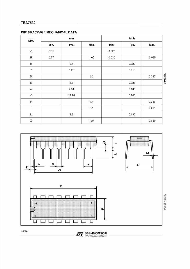
7252019 mXtwxytTDA
httpslidepdfcomreaderfullmxtwxyttda 1517
b 1
c1
s
F
C
GL
E
a 1
a 2
A
e
DM
e3
b
16 9
1 8
P M - S O 1 6 E
P S
SO16 PACKAGE MECHANICAL DATA
DimensionsMillimeters Inches
Min Typ Max Min Typ Max
A 175 0069
a1 01 02 0004 0008
a2 16 0063
b 035 046 0014 0018
b1 019 025 0007 0010
C 05 0020
c1 45o (typ)
D 98 10 0386 0394
E 58 62 0228 0244
e 127 0050
e3 889 0350
F 38 40 0150 0157
G 46 53 0181 0209
L 05 127 0020 0050
M 062 0024
S 8o
(max)
S O 1 6 T
B L
TEA7532
1516
7252019 mXtwxytTDA
httpslidepdfcomreaderfullmxtwxyttda 1617
Information furnished is believed to be accurate and reli able However SGS-THOMSON Microelectronics assumes no responsibility for
the consequences of use of such information nor for any infringement of patents or other rights of third parties which may result from itsuse No license is granted by implication or otherwise under any patent or patent rights of SGS-THOMSON Microelectronics Specifica-tions mentioned i n this publication are subject to change w ithout notice This publication supersedes and replaces all information pre-
viously supplied SGS-THOMSON Microelectronics products are not authorized for use as critical components in l ife support devices orsystems without express written approval of SGS-THOMSON Microelectronics
983209 1994 SGS-THOMSON Microelectronics - All Rights Reserved
SGS-THOMSON Microelectronics GROUP OF COMPANIES
Australia - Brazil - France - Germany - Hong Kong - Italy - Japan - Korea - Malaysia - Malta - Morocco - The NetherlandsSingapore - Spain - Sweden - Switzerland - Taiwan - Thaliand - United Kingdom- USA
TEA7532
1616
7252019 mXtwxytTDA
httpslidepdfcomreaderfullmxtwxyttda 1717
This datasheet has been download from
wwwdatasheetcatalogcom
Datasheets for electronics components
7252019 mXtwxytTDA
httpslidepdfcomreaderfullmxtwxyttda 1617
Information furnished is believed to be accurate and reli able However SGS-THOMSON Microelectronics assumes no responsibility for
the consequences of use of such information nor for any infringement of patents or other rights of third parties which may result from itsuse No license is granted by implication or otherwise under any patent or patent rights of SGS-THOMSON Microelectronics Specifica-tions mentioned i n this publication are subject to change w ithout notice This publication supersedes and replaces all information pre-
viously supplied SGS-THOMSON Microelectronics products are not authorized for use as critical components in l ife support devices orsystems without express written approval of SGS-THOMSON Microelectronics
983209 1994 SGS-THOMSON Microelectronics - All Rights Reserved
SGS-THOMSON Microelectronics GROUP OF COMPANIES
Australia - Brazil - France - Germany - Hong Kong - Italy - Japan - Korea - Malaysia - Malta - Morocco - The NetherlandsSingapore - Spain - Sweden - Switzerland - Taiwan - Thaliand - United Kingdom- USA
TEA7532
1616
7252019 mXtwxytTDA
httpslidepdfcomreaderfullmxtwxyttda 1717
This datasheet has been download from
wwwdatasheetcatalogcom
Datasheets for electronics components

7252019 mXtwxytTDA
httpslidepdfcomreaderfullmxtwxyttda 1717
This datasheet has been download from
wwwdatasheetcatalogcom
Datasheets for electronics components