self-consistent gaas fet models for amplifier design and device diagnostics
TRANSCRIPT
IEEE TRANSACTTONS ON MSCROWAVE THEORY AND TECHNIQUES, VOL. MTT-32, NO, 12, DECEMBER 1984 1573
Self-Consistent GaAs FET Models for AmplifierDesign and Device Diagnostics
WALTER R. CURTICE, SENIOR MEMBER, IEEE, AND RAYMOND L. CAMISA, SENIOR MEMBER, IEEE
Abstract —A procedure has been developed for producing accurate and
unique small-signaf equivalent circuit models for earner-mounted GSAS
FET’s. The procedure utilizes zero drain-source bias S -p:mameter,tests to
determine accurate vafues of carrier perasitics, and dc measurements to
evaluate the FET’s gate, source, and drain resistances. Subsequent S-
parameter measurements at full bias are then used to resolve the FET into
au equivalent circuit model that has only 8 unknown ellements out of a
possible 16. A teclndque for evaluating the frequency range of accurate
data is presented and the FET model shown is useful well above the
maximum frequency of measurement. Examples of devic~? diagnostics are
presented for RCA flip-chip mounted GOAS FET’s.
I. INTRODUCTION
A N ACCURATE DEVICE model based on the mea-
surement of completed wafers is an invaluable tool
for device and amplifier development. Characterization of
the intrinsic and parasitic structure of the FET can be used
to assess the impact of process and mask variations on
device performance. For instance, the effects of varying
gate location and recess depth, source and drain widths,
gate metallization thickness and composition, could be
directly measured. For amplifiers, modeling can be used to
predict device scattering parameters (S-param~eteri) at mil-
limeter-wave frequencies where they cannot be measured
with current commercial equipment. Within the measure-
ment range of network analyzers, these accurate models
can effectively be used to simulate the performance of
matched and combined FET cells to determine optimal
circuit topology.
Previously, attempts to try to construct FET models
were based only on S-parameter measurements. But Vaitus
[1] has shown that the errors associated with measuring
and de-embedding device scattering parameters leads to
significant errors in the equivalent circuit element values
for GaAs FET’s. Some of these errors can be reduced with
improved S-parameter measurement techniques such as the
through, short, delay (TSD) approach [2] and the technique
of Bianco et al. [3], wherein the effects of RF launchers are
accurately removed. However, GaAs power FET’s are car-
rier-mounted and therefore are surrounded by more para-
sitic circuit elements and require additional de-embedding.
Part of the problem is that there are too many variables
to create a unique solution based only upon a set of
Mmuscript receivedApril 30, 1984.The authors are with the Microwave Technology Center, RCA Labora-
tories, Princeton, NJ 08540.
broad-band S-parameter measurements. The situation is
even worse for characterization of GaAs dual-gate FET’s.
Tsironis and Meierer [4] attempt to resolve 28 circuit
element values from 3-port S-parameter data. As they
discuss, the optimization process is hopeless unless started
with accurate estimates of most circuit element values from
independent measurements or calculations.
In this paper, an accurate and unique equivalent circuit
model is developed by using three different automated
measurements of the carrier-mounted FET.
1) The FET mounted in its carrier is measured from
4–20 GHz using a coaxial test fixture where the chip is
only a connector away from the measurement reference
plane where the calibration occurs. A recent improvement
in this technique is the use of electrically short 3.5-mm
connectors. These connections are SMA compatible, low
loss, and resonance free to 34 GHz.
2) The gate (R ~), source (R.), and drain resistances
(Rd) are measured using an automated Fukui approach
[5].
3) Cold FET S-parameter measurements with zero drain-
to-source voltage are used to determine external parasitic
such as wirebound inductance and carrier stand-off capaci-
tance (these measurements must be made just before the
hot S-parameter tests).
With these additional measurements the number of un-
known variables is reduced from a total of 16 to 8, which
makes it much easier to determine an accurate and unique
model for the FET chips that fits the measured data.
Once the modeling procedure has been established, mod-
els are developed for RCA flip-chip FET’s with submi-
crometer T-shape gates [6]. The range of validity of the
model, convergence considerations, and the diagnostic in-
formation obtained for these wafers are discussed.
II. DUMMY PACKAGE MEASUREMENTS
S-parameter measurements were made of 1.4-mm-wide
carriers without FET chips, as shown in Fig. 1. The refer-
ence planes are the sides of the carrier as in the case of thedevice measurements. The S-parameter data for the ATC-S
capacitors (used as stand-offs) showed that the RF capaci-
tance was very close to one half of the value measured by a
low-frequency bridge and well behaved up to 18 GHz.
0018-94180/84/1200-1573$01.00 @1984 IEEE
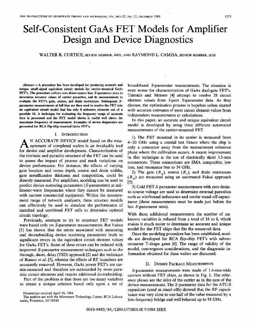
1574 IEEE TRANSACTIONS ON MICROWAVE THEORY AND TECHNIQUES, VOL. MTT-32, NO. 12, DECEMBER 1984
73MIL x 0.5 MlL RIBBON
ATC- SCAPACITOR
c“’’”lL._-.l
r----l k----lcm,Fig. 1. FET carrier model (lower) and cross-sectional view of carrier
(upper).
80[ ,WTti OR WTHOUT C,
01 J
6 8 to 12 14 16 18
FREQUENCY (GHz)
.01t
01 ,
6 8 10 12 14 16 18
FREQuENCY (GHz)
Fig. 2. Amplitude and phase of S12 as a function of frequency for theFET carrier.
The lumped-element model shown in the lower part of
Fig. 1 provides the best agreement with the S-parameter
data for the dummy carrier (i.e., package). The program
SUPER-COMPACT [7] was used to optimize the elementvalues for best agreement with the data. The ribbon lengths
on the two sides are slightly different, but are nominally
0.38 mm. This should produce about 0.20-nH inductance,
which is close to the values measured (Ll = 0.207 nH,
Lz = 0.168 nH). These data show that the pedestal induct-
ance L3 is approximately 20 pH for a pedestal height of
0.30 mm. Fig. 2 shows the amplitude and phase of S12 for
both the model and the measured data. The agreement is
seen to be excellent for the model which Ca is included.
To further study mounting parasitic, other FET carriers
were assembled and S-parameters were measured from 4
to 20 GHz. Table I shows the characteristics of each and
the optimized values of the equivalent circuit components.
TABLE IEQUIVALENT CIRCUIT PARAMETERS FOR DUMMY MESFET
CARRIERS (Cl = Cz = 0.04 pF)
Carrier Width
(mm)
1.4
1.78
1.78
1.78
1.78
1,78
Pedestal
Height (mm) Feature
.30
.30
.30 3 Ribbons
.125
0 Weld
o EPOXY
L L LC
(nH/ (nH~ (p:) (P:)—— —.
0.207 0.168 20.0 0.018
0.224 0.249 19.1 0.011
0.152 0.162 19.7 0.014
0.295 0.313 26.3 0.010
0.160 0,251 17.5 0.011
0.253 0.236 22.8 0.010
It is interesting to note that the pedestal inductance (L3)
measured for the three carriers with 300-pm-high pedestals
is the same value to within 5 percent. L3 is present even
for the zero-high pedestal. This implies that some pedestal
inductance results from mutual inductance between the
gate and drain leads. The geometry of the bond leads in the
pedestal region may thus be important in determining the
pedestal inductance.
The stability factor K for an FET is defined as
A lossless network has a unity value of K. Since we
observed K values much larger than unity in the tests on
the dummy carriers, we believe there are losses associated
with the carrier itself. These losses may arise due to power
dissipation in resistance but it is more likely that they
result from radiation loss,
The agreement between the S-parameters calculated for
the dummy carrier models and the experimental data is
improved if some small loss is assumed in the wire ribbons
and stand-off capacitors. The agreement between S-param-
eters for the carrier-mounted FET’s and their model is
improved slightly with the addition of carrier loss.
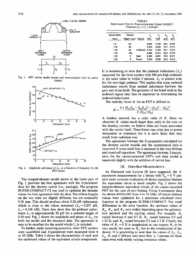
III. ZERO-BIAS MEASUREMENTS
As Diamond and Laviron [8] have suggested, the S-
parameter measurements for a device with Vd~= O V per-
mits more accurate evaluation of device parasitic because
the equivalent circuit is much simpler. Fig. 3 shows the
lumped-element equivalent circuit of the carrier-mounted
FET for the case of zero biasing. Using S-parameter data
for device B1824-20C from 4 to 18 GHz, all circuit element
values were optimized for a minimum calculated error
function in the program SUPER-COMPACT. For small
differences in the error function, the optimum values of
R ~, R,, and R ~ vary widely depending upon the optimiza-
tion method and the starting values. For example, R,
varied between O and 0.7 Q, R ~ varied between 0.9 and
1.53 Q, and R~ varied between 0.5 and 1.3 !2. Clearly, the
value of R, = O i2 is nonphysical as one expects R, to be
very nearly the same as R ~ due to the construction of the
device. It is interesting to note that the values of L,, Ld,
Lg, R, and C did not vary more than + 1 percent for these
cases even with widely varying resistance values.
CURTICE AND CAMISA: SELF-CONSISTENT GAAS FET MODELS 1575
GATELEAD
SOURCELEAO
Fig. 3. Equivalent circuit of carrier-mounted FET at zero drain-source
bias voltage.
TABLE II
OPTIMIZSD CIRCUIT ELEMSNT VALUSS FOR FET 1824-20C WITH
Vd, = O V FOR 4-18 GHz RANGE WITH R = 0.5490,R, =1.048 fl, Rd =1.367 Q, Cl= 0.&4 pF,
Cz = 0.039 pF
%s R c % k Ld k(v) (Q) (PF) (PF) (nH) (nH) (PH)—— —— —.. —
o. .33s4 .2289 .1730 .3115 .2514 10.71-1. .5143 .1814 .1726 .3134 .2507 10.73-2. .7593 .1620 .1725 .3158 .2516 10.46 ‘
To resolve this accuracy problem, we use resistance
values determined from dc measurements of the type de-
scribed by Fukui. These resistance values give the best
approximation available. Using these values, Table II shows
the values of the other circuit elements for three values of
Vg. for V&= O. The values of R and C vary with gate biasas expected and the inductive circuit elemlents’ vary less
thrm 2 percent. The calculated S-parameters for this opti-
mized model are extremely close to the measured data. The
values R and C are not used for subsequent modeling at
full bias but may be used for diagnostic information about
the gate and the conduction channel.
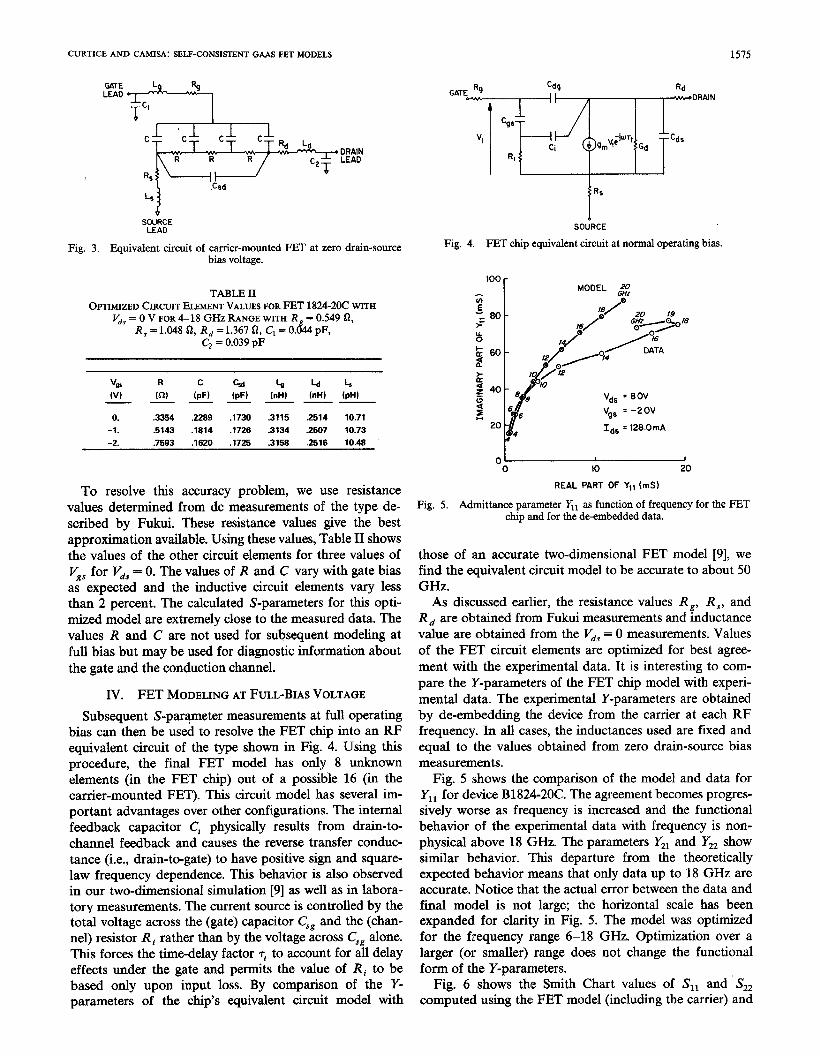
IV. FET MODELING AT FULL-BIAS VOLTAGE
Subsequent S-par~eter measurements at full operating
bitts can then be used to resolve the FET chip into an RF
equivalent circuit of the type shown in Fig. 4. Using this
procedure, the final FET model has only 8 unknown
elements (in the FET chip) out of a possible 16 (in the
carrier-mounted FET). This circuit model has several im-
portant advantages over other configurations. The internal
feedback capacitor Cj physically results from drain-to-
channel feedback and causes the reverse transfer conduc-
tance (i.e., drain-to-gate) to have positive sign and square-
law frequency dependence. This behavior is also observed
in our two-dimensional simulation [9] as well as in labora-
tory measurements. The current source is controlled by thetotal voltage across the (gate) capacitor C.g and the (chan-
nel) resistor R i rather than by the voltage across C~g alone.
This forces the time-delay factor ~, to account for all delay
effects under the gate and permits the value of Ri to be
based only upon input loss. By comparison of the Y-
parameters of the chip’s equivalent circuit model with
“TER:lcfiw*
IRS
SOURCE
Fig. 4. FET thip equivalent circuit at normal operating bias.
V*S = 8 Ov
Vgs = -20V
IdS s 128.OmA
o~o 10 20
REAL PART OF Y,l (mS)
Fig. 5. Admittance parameter Yll as function of frequency for the FETchip and for the de-embedded data.
those of an accurate two-dimensional FET model [9], wefind the equivalent circuit model to be accurate to about 50
GHz.
As discussed earlier, the resistance values Rg, R,, and
Rd are obtained from Fukui measurements and inductance
value are obtained from the V~, = O measurements. Values
of the FET circuit elements are optimized for best agree-
ment with the experimental data. It is interesting to com-
pare the Y-parameters of the FET chip model with experi-
mental data. The experimental Y-parameters are obtained
by de-embedding the device from the carrier at each RF
frequency. In all cases, the inductances used are fixed and
equal to the values obtained from zero drain-source bias
measurements.
Fig. 5 shows the comparison of the model and data for
Yll for device B1824-20C. The agreement becomes progres-
sively worse as frequency is increased and the functional
behavior of the experimental data with frequency is non-
physical above 18 GHz. The parameters Y21 and Yzz show
similar behavior. This departure from the theoretically
expected behavior means that only data up to 18 GHz are
accurate. Notice that the actual error between the data and
final model is not large; the horizontal scale has been
expanded for clarity in Fig. 5. The model was optimized
for the frequency range 6–18 GHz. Optimization over a
larger (or smaller) range does not change the functional
form of the Y-parameters.
Fig. 6 shows the Smith Chart values of &l and S22
computed using the FET model (including the carrier) and

1576 IEEE TRANSACTIONS ON MICROWAVE THEORY AND TECHNIQUES, VOL. MTT-32, NO. 12, DECEMBER 1984
0
A = MEASURED Vd~ =8 OV
o = MOOEL Vw =-20V
I*= 1280mA
Fig. 6. Smith Chart display ofmeasured dataandmodel for&l and S22for the carrier-mounted FET.
A = MEASURED
0: MODELvd~ = 8 Ov
Vgs ‘ -20V
Ids = 1280mA
Fig. 7. Smith Chart display of S12.
the measured data. The errors are cleady more apparent in
Fig. 5 than in Fig. 6. Figs. 7 and 8 show Slz and Szl,
respectively. Errors are small. FET’s measured and mod-
eled a second time (after disassembly from the test fixture)
show only small changes in the values of equivalent circuit
elements. Table III shows the percentage change in each
circuit element value. The circuit elements R ~ and C, are
not well resolved by the data set but do not affect the
maximum available gain (MAG) greatly. Notice that ~~,
~MAX, and K are not greatly changed upon remeasurement.
V. CONVERGENCE CONSIDERATIONS
SUPER-COMPACT is extremely useful for evaluating
the values of the equivalent circuit for best agreement with
the measured data. However, some element values are not
uniquely determined and the resulting value is a function
of the search technique. We have addressed this problem
by minimizing the number of elements permitted to vary.
Using the procedures described earlier, our final FET
model has only 8 variable elements, out of a total of 16.
A = MEASURED. . MODEL Vd~ = 8 OV
%= –20V
Ids= 128 OrnA
Fig. 8. Smith Chart display of S21.
TABLE III
EQUIVALENT CIRCUIT ELEMENT VALUSS FOR Two SEPARATE
MEASUREMENTS OF Two FET’s AND PERCENTAGE CHANGES(DATA USED FOR 6-18 GHz WITH Vd, = 8 V, VVd, = -210
$ET ld, 9“ r~o.,
H, % $ %, % k.(~ p+ * Q ~ I@— @ Jg & {$Hz] [GHz) :
8188997 9s0 #699 8186 3262 2274 01385 466 2587 114 101 350 223
Rmam,ed 950 4270 8074 3123 2500 06874 470 2281 813 99 3d 3 220
B182420C 1280 4211 7405 3164 1088 0,6870 100 4157 190,0 98 352 205
Rema,wred 1270 ~ ~ ~ p& 06631 149 4042 1930 ~ ~ ~
w % Chmw 80 44 41 160 55 250 19 39 20 bo 48Rma’”red
The problem of unequivocally determining the optimum
values of the equivalent circuit elements is not trivial. After
extensive investigation, we have found that:
1) optimization should be done with the fewest possible
unknown circuit elements;
2) Both random number of gradient search techniques
should be used to assure that the results are convergent
and independent of the starting values;
3) some circuit element values may never converge for
certain data sets;
4) convergence of the important circuit elements occurs
early in the search.
VI. EVALUATION OF~u
The frequency of O-dB maximum available gain (MAG)
~- is often evaluated using analytical expressions de-
rived with simplifying assumptions. The most accurate
value is obtained by extrapolating the FET chip model
(i.e., the de-embedded chip), in frequency using SUPER-
COMPACT because the simplifying assumptions are often
not valid for real devices. For accuracy, it is necessary to
achieve good agreement between the model and data for
the stability factor (as well as for S-parameters) over the
range of measurement. MAG strongly depends upon the
stability factor.
Fig. 9 shows an example of the effect of carrier losses for
an FET of 600-pm periphery from wafer B1824. The figure

CURIICE AND CAMISA : SELF-CONSISTENT GAAS FET MODELS 1577
/LOSSY “CARRIER-
/bz
/’~ , FIRST MEASUREMENT A 0
. . SECONDMEASUfiEMENT
J
Ao
/
#
A
~LOSSLE8S
>0:0 cAm’ERAil@oO
~do o
oo~a
FREWENCY (GHz )
Fig. 9. Stability factor ss a function of frequency for the measured data
and for the models.
shows the stability factor obtained from the data for two
separate measurements and from the mbdel for the
MESFET carrier with and without loss. The agreement is
seen to be better for the lossy carrier. The optimum value
of added loss is 100 0 in series with capacitors Cl and ?Z
shown in Fig. 1. The value of ~- obtained for the chip
alone for either case is 34.0 GHz. However, for some cases,
the addition of loss to the carrier improves the. model such
that the value of ~u is altered.
VII. DIAGNOSTIC INFO*TION PROEWCED
BY MODELS
A group of GaAs FET’s from six different wafers were
characterized to determine the relationship between device
parameters and RF performance. All devices are flip-chip
mounted and have 600-pm source periphery and ap-
pro~mately l-pm gate length. The dc parameters were
measured using the automated Fukui method, and S-
parameter measurements were made by our method from 4
to 20 GHz. Lumped-element circuit models were con-
structed for each device using the procedure described. We
present a summarized version of this data for comparison
of the wafers.
Table IV shows results from several devices from six
wafers. The Fukui pinchoff voltage is measured at small
drain-source voltages in the linear regions and is always
less than that measured above current saturation. The
average N. a product (donor-thickness product) is obtained
by averaging tlie value from the Fukui measurement (from
maximum dc channel currents) and the value from RF
capacitance measurements. The errors involved in de-
termining the N“ a product from the Fukui data alone
make the value smaller while the errors involved in the RF
measurement make the value large. The average of these
N. a values is thus more accurate.
The average donor value N is calculated from the aver-
age N. a product and the pinchoff voltage. The donor
values czilculated in this manner are generally larger than
measured in profiling the wafer but are believed to be more
TABLE IV
SUMMARY OF DC AND RF TEST RESULTS FOR 12 FET’S(RF TESTS h4ADE AT V((, = 8 V, V’, = -2 V)
Fukui Average AveragePinch.Off N.a N ft ‘MAX ‘Sdb (LS)
Device (v) (llD12cm”2) (1017 cm-3) (GHz) (GHz) (GHz).— — ——
B1271-A54
B1824-lC
a
C1851-11
-3
B1512-lA
-2A
E627-64
-65
-2
B1832-17
-16
3.66
4.94
5.56
4.35
3.0
2.5
3.5
6.27
8.11
5.0
5.62
5.81
3.45
4.124.02
3.893.354.264.154.053,85
3.75
5.15.7
1.9 12.7 41.2 32,3
2.2 9.8 36.0 26.5
1.9 10.3 34.0 27.0
2.2 10.1 34.4 22.0
2.2 12.0 36.0 25.0
4.0 9.0 32.0 22.6
2.9 8.75 32.0 22.0
1.7 8.75 32.5 18.0
1.6 8.80 32.0 18.5
1.8 10.0 32.0 21.6
3.0 7.7 30.5 17.5
3.0 8.0 29.6 17.6
-25 0 +25
PERCENTAGE CHANGE
Fig. 10. Maximum available gain as a function of percentage change in
value of model elements for FET B1824-20C at Vd, = 8 V, V& = – 2 V.
accurate because they are more compatible with device ‘
performance.
The current cutoflf frequency f, is calculated from the
ratio of transconductance to gate-source capacitance using
the equivalent circuit model. The fW is obtained by
extrapolating’ the FET chip model in frequency using
SUPER-COMPACT,, Finally, ~~~~ (LS), the frequency of
3-dB maximum available gain under optimum large-signal
loading, is evaluated using SUPER-COMPACT for the
FET chip with a net IIoad conductance of G~ = 10/(VO – 1),
where 10 = drain-source current and V. = drain-source
voltage.
Notice that both ~W and ~q~~ (LS) depend directly
upon ft. Thus, ft should be maximized for the highest
operating frequency. Notice also that although the range in
fw is small (6 GHz) the range in f3dB (LS) is signifi-
cantly larger (9.5 GH[z). This reflects the fact that the dc as
well as the RF quantities determine the maximum frequency
for useful operation of power FET’s.The largest values of f3dB (LS) occur most frequently for
the FET’s with Fukui pinchoff voltages in the range of 3 to
5 V. Four devices with pinchoff voltages near 6 V have
significantly lower values of ja~~ (LS). There is no ap-
parent correlation between ~~~~ (LS) and N. a product or
N value. The value of fw of the device from wafer
1578 IEEE TRANSACTIONS ON MICROWAVE THEORY AND TECHNIQUES, VOL. MTr-32, NO. 12, DECEMBER 1984
B1271 is exceptionally high primarily due to the exception-
ally small value of drain-ghte capacitance.
To evaluate the influence of each FET parameter upon
performance, calculations were made of the MAG at 20
GHz for parameter changes of O, +25 percent, and – 25
percent for device B1824-20C. Fig. 10 shows the results of
this study. The largest improvement (2.0 dB) occurs for
increased transconductance ( g~ ). The decrease in transit-
time ( ~f) or drain-gate capacitance (Cdg) improves the
MAG by about 0.8 and 0.9 dB, respectively. An increase in
R~~ or a decrease in R~, Rg, or Ri all result in less than
0.5-dB improvement. The most significant improvement in
device performance will be made by increasing g~ and
reducing Tt and Cdg.
VIII. CONCLUSION
A procedure has been developed for producing equiv-
alent circuit models for carrier-mounted GRAS FET’s for
both device design and diagnostic purposes. A prominent
feature of this procedure is the reduction of the number of
unknown element values to be determined by S-parameter
data, by the use of dc measurements as well as zero-bias
measurements. The zero-bias data are used to evaluate the
circuit inductances and are taken just before the full-bias
data.
It was shown that agreement for S-parameters does not
assure agreement for the values of stability factor and
MAG. Loss in the FET carrier will affect the values
determined for the circuit elements which model the FET
chip.
The equivalent circuit models were used to evaluate a
group of GaAs MESFET’S. The conduction channel
parameters were calculated and the frequency response
characteristics were predicted.
ACKNOWLEDGMENT
The authors wish to thank P. D. Gardner (RCA Labora-
tories) and Y.-H. Yun (now with MA/COM, Inc.) for
implementation of the automated Fukui measurements.
[1]
[2]
[3]
[4]
[5]
[6]
[7]
REFERENCES
R. L. Vaitus, “Uncertainty in the values of GaAs MESFET equiv-alent circuit elements extracted from iiteasured two-port scatteringparameters,” presented at 1983 IEEE Cornell Conference on High
Speed Semiconductor Devices and Circuits, Cornell Un., Aug. 1983.R. A. Speciale, “A generalization of the TSD network-analyzercalibration procedure, covering n-port scattering-parameter measure-ments, affected by leakage errors,” IEEE Trans. Microwave Theo~Tech., vol. MTT-25, pp. 11OC-1115, Dec. 1977.B. Biauco et al., “Launcher and microstrip characterization,” IEEETrans. Inswum. Mess., vol. IM-25, no. 4, pp. 320-323.
C. Tsironis and R. Meierer, “Microwave wide-band model of GaAsduaf gate MESFET’s~ IEEE Trans. Microwave Theory Tech., vol.MTT-30, pp. 243-251, Mar. 1982.H. Fukui, “Determinations of the basic parameters of a GaAsMESFET,” Bell Syst. Tech. J., vol. 58, no. 3, Mar. 1979.
G. C. Taylor et al., “ GaAs power field-effect transistors for K-bandoperation,” RCA Rev., vol. 42, no. 4, pp. 508-521, Dec. 1981.
SUPER-COMPACT, Linear Circuit Analysis and Optimization,Compact Engineering, Pafo Afto, CA, 1981.
[8]
[9]
F. Diamond and M. Laviron, “Measurement of the extrensic serieselements of a microwave MESFET under zero current conditions,” in
Proc. 12th European A4icrowaue Conf., (Finland), Sept. 1982.
W. R. Curtice, “The performance of submicron gate length GaAs
MESFETS:’ IEEE Trans. Electron Devices, vol. ED-30, pp.
1693–1699, Dec. 1983.
*
Wafter R. Curtice (M58–SM69) received theB. E. E., M. S., and Ph.D. degrees from Cornell
University in 1958, 1960, and 1962, respectively.
The subject of his Master’s thesis was the ruby
maser; research for his doctoraf thesis was con-
cerned with noise in linear-beam microwave de-
vices.In 1962, he joined the Raytheon Microwave
and Power Tube Division as a Senior Researchand Development Engineer. He participated inmicrowave tube develot)ment and l)erformed ex-
perimental and theoretical research on linew-beam and &oss-field de-vices. In 1967, he became Visiting Assistant Professor of ElectricalEngineering at the University of Michigan, and in 1969 was appointed
Associated Professor. In addition to teaching courses on physicaJ electron-
ics and microwave measurements, he was engaged in sponsored research
on microwave semiconductors with emphasis on transferred-electron de-vices.
In 1973, Dr. Curtice joined RCA Laboratones, Princeton, NJ, as a
Member of the Technical Staff, in the Microwave Technology Center. For
severaf years he directed the development of second-harmonic-extractionTRAPATT amplifiers for X-band operation. He has developed two-
dimensional computer models of GaAs transferred-electron logic devicesand field-effect transistors and computer simulation programs useful inthe development of gigabit-rate GSAS and GaInAs integrated circuits. Heis presently directing small-signal and large-signal FET modefing pro-
grams.Dr. Curtice has authored over 40 technicaf papers and has eight U.S.
patents issued to him. He is also a member of Tau Beta Pi, Eta KappaNu, and Sigma Xi. He was Chairman of IEEE’s Boston Section of theElectron Devices group from 1966 to 1967, and Chairman of the South-
eastern Michigan Section of the combined MTT, ED, and AP groups for
1972.
Raymond L. Camisa (M’68–SM’83) received theB. E. E., M. E. E., and Ph.D. degrees from the City
University of New York in 1965, 1969, and 1974,respectively.
In 1974, he joined the Microwave Technology
Center at RCA Laboratories, Princeton, NJ. Hisresponsibilities include ieseirch on GaAs field-
effect transistor devices and circuits. As ,a mem-
ber of a technicaf team, he contributed to the
development of the first l-W, X-band powertransistor in 1974. In 1979, he received an RCA
Laboratories Outstanding Achievement Award for the development of
microwave lumped-element broad-band FET power amplifiers and milli-meter-wave transistors and circuits.
He has published more than 20 papers on low-noise parametric ampli-fiers, microwave integrated circuits, MIS varactors, and Ga.As FE’_f
amplifiers, oscillators, ~d devices. He currently holds five U.S. patents.As an active member of IEEE, Dr. Camisa has served on many local
and regional committees. He is a founder and past Chairrmm of thePrinceton Area Microwave Theory and Techniques and Electron Devices
(MTT/ED) Chapter. He afso was Chairman of the IEEE Princeton
Section and, subsequently, of the IEEE Metropolitan Societies ActivitiesCouncil (METSAC), which coordinates the activities of afl IEEE groupsin the New York, New Jersey, and Connecticut tri-state area. He is aDirector of ELECTRO, the ltigest electronics technicaf and marketingshow in the East, and was the Convention Director of ELECTRO ’83.